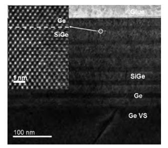
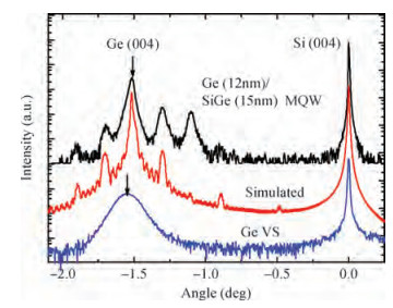
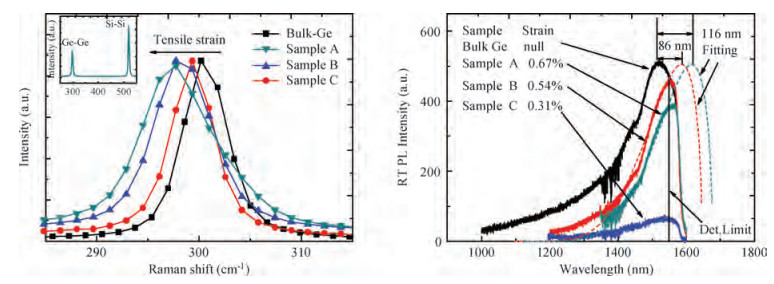
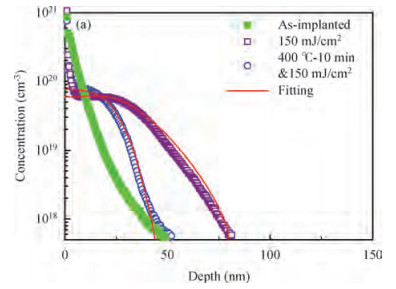
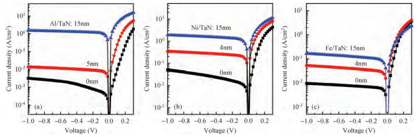
Fig. 1.
(Color online) Typical HRTEM and AFM images of Ge on Si grown by two-step growth techniques[13].
INVITED REVIEW PAPERS
Buwen Cheng1, , Cheng Li2, Zhi Liu1 and Chunlai Xue1
Corresponding author: Cheng Buwen, Email: cbw@semi.ac.cn
Abstract: Si-based germanium is considered to be a promising platform for the integration of electronic and photonic devices due to its high carrier mobility, good optical properties, and compatibility with Si CMOS technology. However, some great challenges have to be confronted, such as: (1) the nature of indirect band gap of Ge; (2) the epitaxy of dislocation-free Ge layers on Si substrate; and (3) the immature technology for Ge devices. The aim of this paper is to give a review of the recent progress made in the field of epitaxy and optical properties of Ge heterostructures on Si substrate, as well as some key technologies on Ge devices. High crystal quality Ge epilayers, as well as Ge/SiGe multiple quantum wells with high Ge content, were successfully grown on Si substrate with a low-temperature Ge buffer layer. A local Ge condensation technique was proposed to prepare germanium-on-insulator (GOI) materials with high tensile strain for enhanced Ge direct band photoluminescence. The advances in formation of Ge n+p shallow junctions and the modulation of Schottky barrier height of metal/Ge contacts were a significant progress in Ge technology. Finally, the progress of Si-based Ge light emitters, photodetectors, and MOSFETs was briefly introduced. These results show that Si-based Ge heterostructure materials are promising for use in the next-generation of integrated circuits and optoelectronic circuits.
Keywords: Ge, Ge-on-insulator, Si-based, epitaxy, light emitting diode, photodetector, MOSFET
| [1] |
Claeys C, Simoen E. Germanium based technologies: from materials to devices. Amsterdam: Elsevier, 2007
|
| [2] |
Kang Y, Liu H D, Morse M, et al. Monolithic germanium/silicon avalanche photodiodes with 340 GHz gain-bandwidth product. Nature Photonics, 2008, 3: 59 http://cn.bing.com/academic/profile?id=2155130433&encoded=0&v=paper_preview&mkt=zh-cn
|
| [3] |
Li C, Xue C, Liu Z, et al. High-bandwidth and high-responsivity top-illuminated germanium photodiodes for optical interconnection. IEEE Trans Electron Devices, 2013, 60(3): 1183 doi: 10.1109/TED.2013.2241066
|
| [4] |
Vivien L, Polzer A, Marris-Morini D, et al. Zero-bias 40 Gbit/s germanium waveguide photodetector on silicon. Optics Express, 2012, 20: 1096 doi: 10.1364/OE.20.001096
|
| [5] |
Kuo Y H, Lee Y K, Ge Y, et al. Strong quantum-confined Stark effect in germanium quantum-well structures on silicon. Nature, 2005, 437: 1334 doi: 10.1038/nature04204
|
| [6] |
Roth J E, Fidaner O, Schaevitz R K, et al. Optical modulator on silicon employing germanium quantum wells. Opt Express, 2007, 15: 5851 doi: 10.1364/OE.15.005851
|
| [7] |
Hu W X, Cheng B W, Xue C L, et al. Electroluminescence from Ge on Si substrate at room temperature. Appl Phys Lett, 2009, 95: 092102 doi: 10.1063/1.3216577
|
| [8] |
Liu J, Sun X, Aguilera R, et al. Ge-on-Si laser operating at room temperature. Opt Lett, 2010, 35: 679 doi: 10.1364/OL.35.000679
|
| [9] |
Shang H, Okorn-Schimdt H, Ott J, et al. Electrical characterization of germanium p-channel MOSFETs. IEEE Electron Device Lett, 2003, 24(4): 242 doi: 10.1109/LED.2003.810879
|
| [10] |
Morii K, Iwasaki T, Nakane R, et al. High performance GeO2/Ge nMOSFETs with source/drain junctions formed by gas phase doping. IEEE International Electron Devices Meeting (IEDM), 2009: 1 http://cn.bing.com/academic/profile?id=2108485420&encoded=0&v=paper_preview&mkt=zh-cn
|
| [11] |
Currie M T, Samavedam S B, Langdo T A, et al. Controlling threading dislocation densities in Ge on Si using graded SiGe layers and chemical-mechanical polishing. Appl Phys Lett, 1998, 72(14): 1718 doi: 10.1063/1.121162
|
| [12] |
Luan H C, Lim D R, Lee K K, et al. High-quality Ge epilayers on Si with low threading-dislocation densities. Appl Phys Lett, 1999, 75(19): 2909 doi: 10.1063/1.125187
|
| [13] |
Huang Shihao, Li Cheng, Zhou Zhiwen, et al. Depth-dependent etch pit density in Ge epilayer on Si substrate with a selfpatterned Ge coalescence island template. Thin Solid Films, 2012, 520: 2307 doi: 10.1016/j.tsf.2011.09.023
|
| [14] |
Chen Y H, Li C, Zhou Z W, et al. Room temperature photoluminescence of tensile-strained Ge/Si0:13Ge0:87 quantum wells grown on silicon-based germanium virtual substrate. Appl Phys Lett, 2009, 94(14): 141902 doi: 10.1063/1.3114408
|
| [15] |
Chen Y H, Li C, Lai H K, et al. Quantum-confined direct band transitions in tensile strained Ge/SiGe quantum wells on silicon substrate. Nanotechnology, 2010, 21: 115207 doi: 10.1088/0957-4484/21/11/115207
|
| [16] |
Li C, Chen Y H, Zhou Z W, et al. Enhanced photoluminescence of strained Ge with a delta-doping SiGe layer on silicon and siliconon-insulator. Appl Phys Lett, 2009, 95: 251102 doi: 10.1063/1.3275863
|
| [17] |
Tezuka T, Sugiyama N, Takagi S. Fabrication of strained Si on an ultrathin SiGe-on-insulator virtual substrate with a high-Ge fraction. Appl Phys Lett, 2001, 79(12): 1798 doi: 10.1063/1.1404409
|
| [18] |
Hu Meijiao, Li Cheng, Xu Jianfang, et al. Formation and properties of GeOI prepared by cyclic thermal oxidation and annealing processes. Acta Phys Sin, 2011, 60(7): 078102 http://cn.bing.com/academic/profile?id=1632909217&encoded=0&v=paper_preview&mkt=zh-cn
|
| [19] |
Huang S H, Lu W F, Li C, et al. A CMOS-compatible approach to fabricate an ultra-thin germanium-on-insulator with large tensile strain for Si-based light emission. Optics Express, 2013, 21(1): 640 doi: 10.1364/OE.21.000640
|
| [20] |
Wang C, Li C, Huang S H, et al. Low specific contact resistivity to n-Ge and well-behaved Ge n+/p diode achieved by implantation and excimer laser annealing. Appl Phys Express, 2013, 6: 106501 doi: 10.7567/APEX.6.106501
|
| [21] |
Huang S H, Li C, Chen C Z, et al. In situ doped phosphorus diffusion behavior in germanium epilayer on silicon substrate by ultra-high vacuum chemical vapor deposition. Appl Phys Lett, 2013, 102: 182102 doi: 10.1063/1.4804204
|
| [22] |
Wang C, Li C, Lin G Y, et al. Germanium n(+)/p shallow junction with record rectification ratio formed by low-temperature preannealing and excimer laser annealing. IEEE Trans Electron Devices, 2014, 61(9): 3060 doi: 10.1109/TED.2014.2332461
|
| [23] |
Zhou Y, Ogawa M, Han X H, et al. Alleviation of Fermi level pinning effect on metal/germanium interface by insertion of an ultrathin aluminum oxide. Appl Phys Lett, 2008, 93(20): 202105 doi: 10.1063/1.3028343
|
| [24] |
Kobayashi M, Kinoshita A, Saraswat K, et al. Fermi-level depinning in metal/Ge Schottky junction and its application to metal source/drain Ge NMOSFET. Symp VLSI Tech Symp, 2008: 54 http://cn.bing.com/academic/profile?id=2103845540&encoded=0&v=paper_preview&mkt=zh-cn
|
| [25] |
Nishimura T, Kita K, Toriumi A. A significant shift of Schottky barrier heights at strongly pinned metal/germanium interface by inserting an ultra-thin insulating film. Appl Phys Express, 2008, 1: 051406 doi: 10.1143/APEX.1.051406
|
| [26] |
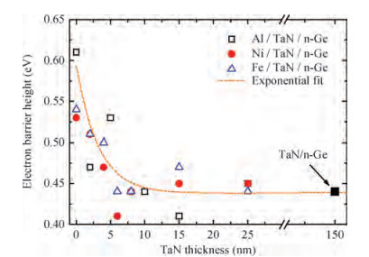
Wu Z, Huang W, Li C, et al. Modulation of Schottky barrier height of metal/TaN/n-Ge junctions by varying TaN thickness. IEEE Trans Electron Devices, 2012, 59(9): 1328 http://cn.bing.com/academic/profile?id=1999355566&encoded=0&v=paper_preview&mkt=zh-cn
|
| [27] |
Dimoulas A, Tsipas P, Sotiropoulos A, et al. Fermi level pinning and charge neutrality level in germanium. Appl Phys Lett, 2006, 89(25): 252110 doi: 10.1063/1.2410241
|
| [28] |
Wu H D, Huang W, Lu W F, et al. Ohmic contact to n-type Ge with compositional Ti nitride. Appl Surf Sci, 2013, 284: 877 doi: 10.1016/j.apsusc.2013.08.028
|
| [29] |
Wu H D, Wang C, Wei J B, et al. Ohmic contact to n-type Ge with compositional W nitride. IEEE Electron Device Lett, 2014, 35(12): 1188 doi: 10.1109/LED.2014.2365186
|
| [30] |
Sun X C, Liu J F, Kimerling L C, et al. Room-temperature direct bandgap electroluminesence from Ge-on-Si light-emitting diodes. Opt Lett, 2009, 34(8): 1198 doi: 10.1364/OL.34.001198
|
| [31] |
Hu W X, Cheng B W, Xue C L, et al. Electroluminescence from Ge on Si substrate at room temperature. Appl Phys Lett, 2009, 95: 092102 doi: 10.1063/1.3216577
|
| [32] |
Cheng S L, Lu J, Shambat G, et al. Room temperature 1.6 melectroluminescence from Ge light emitting diode on Si substrate. Optics Express, 2009, 17(12): 10019 doi: 10.1364/OE.17.010019
|
| [33] |
Liu J F, Sun X C, Camacho-Aguilera R, et al. Ge-on-Si laser operating at room temperature. Opt Lett, 2010, 35(5): 679 doi: 10.1364/OL.35.000679
|
| [34] |
Camacho-Aguilera R E, Cai Y, Patel N, et al. An electrically pumped germanium laser. Optics Express, 2012, 20(10): 11316 doi: 10.1364/OE.20.011316
|
| [35] |
Koerner R, Oehme M, Gollhofer M, et al. Electrically pumped lasing from Ge Fabry-Perot resonators on Si. Optics Express, 2015, 23(11): 14815 doi: 10.1364/OE.23.014815
|
| [36] |
Xue H Y, Xue C L, Cheng B W, et al. Zero biased Ge-on-Si Photodetector with a bandwidth of 4.72 GHz at 1550 nm. Chin Phys B, 2009, 18(6): 2542 doi: 10.1088/1674-1056/18/6/070
|
| [37] |
Li C, Xue C L, Liu Z, et al. High-bandwidth and highresponsivity top-illuminated germanium photodiodes for optical interconnection. IEEE Trans Electron Devices, 2013, 60(3): 1183 doi: 10.1109/TED.2013.2241066
|
| [38] |
Li Chong, Xue Chunlai, Li Yaming, et al. High performance silicon waveguide germanium photodetector. Chin Phys B, 2015, 24(3): 038502 doi: 10.1088/1674-1056/24/3/038502
|
| [1] |
Claeys C, Simoen E. Germanium based technologies: from materials to devices. Amsterdam: Elsevier, 2007
|
| [2] |
Kang Y, Liu H D, Morse M, et al. Monolithic germanium/silicon avalanche photodiodes with 340 GHz gain-bandwidth product. Nature Photonics, 2008, 3: 59 http://cn.bing.com/academic/profile?id=2155130433&encoded=0&v=paper_preview&mkt=zh-cn
|
| [3] |
Li C, Xue C, Liu Z, et al. High-bandwidth and high-responsivity top-illuminated germanium photodiodes for optical interconnection. IEEE Trans Electron Devices, 2013, 60(3): 1183 doi: 10.1109/TED.2013.2241066
|
| [4] |
Vivien L, Polzer A, Marris-Morini D, et al. Zero-bias 40 Gbit/s germanium waveguide photodetector on silicon. Optics Express, 2012, 20: 1096 doi: 10.1364/OE.20.001096
|
| [5] |
Kuo Y H, Lee Y K, Ge Y, et al. Strong quantum-confined Stark effect in germanium quantum-well structures on silicon. Nature, 2005, 437: 1334 doi: 10.1038/nature04204
|
| [6] |
Roth J E, Fidaner O, Schaevitz R K, et al. Optical modulator on silicon employing germanium quantum wells. Opt Express, 2007, 15: 5851 doi: 10.1364/OE.15.005851
|
| [7] |
Hu W X, Cheng B W, Xue C L, et al. Electroluminescence from Ge on Si substrate at room temperature. Appl Phys Lett, 2009, 95: 092102 doi: 10.1063/1.3216577
|
| [8] |
Liu J, Sun X, Aguilera R, et al. Ge-on-Si laser operating at room temperature. Opt Lett, 2010, 35: 679 doi: 10.1364/OL.35.000679
|
| [9] |
Shang H, Okorn-Schimdt H, Ott J, et al. Electrical characterization of germanium p-channel MOSFETs. IEEE Electron Device Lett, 2003, 24(4): 242 doi: 10.1109/LED.2003.810879
|
| [10] |
Morii K, Iwasaki T, Nakane R, et al. High performance GeO2/Ge nMOSFETs with source/drain junctions formed by gas phase doping. IEEE International Electron Devices Meeting (IEDM), 2009: 1 http://cn.bing.com/academic/profile?id=2108485420&encoded=0&v=paper_preview&mkt=zh-cn
|
| [11] |
Currie M T, Samavedam S B, Langdo T A, et al. Controlling threading dislocation densities in Ge on Si using graded SiGe layers and chemical-mechanical polishing. Appl Phys Lett, 1998, 72(14): 1718 doi: 10.1063/1.121162
|
| [12] |
Luan H C, Lim D R, Lee K K, et al. High-quality Ge epilayers on Si with low threading-dislocation densities. Appl Phys Lett, 1999, 75(19): 2909 doi: 10.1063/1.125187
|
| [13] |
Huang Shihao, Li Cheng, Zhou Zhiwen, et al. Depth-dependent etch pit density in Ge epilayer on Si substrate with a selfpatterned Ge coalescence island template. Thin Solid Films, 2012, 520: 2307 doi: 10.1016/j.tsf.2011.09.023
|
| [14] |
Chen Y H, Li C, Zhou Z W, et al. Room temperature photoluminescence of tensile-strained Ge/Si0:13Ge0:87 quantum wells grown on silicon-based germanium virtual substrate. Appl Phys Lett, 2009, 94(14): 141902 doi: 10.1063/1.3114408
|
| [15] |
Chen Y H, Li C, Lai H K, et al. Quantum-confined direct band transitions in tensile strained Ge/SiGe quantum wells on silicon substrate. Nanotechnology, 2010, 21: 115207 doi: 10.1088/0957-4484/21/11/115207
|
| [16] |
Li C, Chen Y H, Zhou Z W, et al. Enhanced photoluminescence of strained Ge with a delta-doping SiGe layer on silicon and siliconon-insulator. Appl Phys Lett, 2009, 95: 251102 doi: 10.1063/1.3275863
|
| [17] |
Tezuka T, Sugiyama N, Takagi S. Fabrication of strained Si on an ultrathin SiGe-on-insulator virtual substrate with a high-Ge fraction. Appl Phys Lett, 2001, 79(12): 1798 doi: 10.1063/1.1404409
|
| [18] |
Hu Meijiao, Li Cheng, Xu Jianfang, et al. Formation and properties of GeOI prepared by cyclic thermal oxidation and annealing processes. Acta Phys Sin, 2011, 60(7): 078102 http://cn.bing.com/academic/profile?id=1632909217&encoded=0&v=paper_preview&mkt=zh-cn
|
| [19] |
Huang S H, Lu W F, Li C, et al. A CMOS-compatible approach to fabricate an ultra-thin germanium-on-insulator with large tensile strain for Si-based light emission. Optics Express, 2013, 21(1): 640 doi: 10.1364/OE.21.000640
|
| [20] |
Wang C, Li C, Huang S H, et al. Low specific contact resistivity to n-Ge and well-behaved Ge n+/p diode achieved by implantation and excimer laser annealing. Appl Phys Express, 2013, 6: 106501 doi: 10.7567/APEX.6.106501
|
| [21] |
Huang S H, Li C, Chen C Z, et al. In situ doped phosphorus diffusion behavior in germanium epilayer on silicon substrate by ultra-high vacuum chemical vapor deposition. Appl Phys Lett, 2013, 102: 182102 doi: 10.1063/1.4804204
|
| [22] |
Wang C, Li C, Lin G Y, et al. Germanium n(+)/p shallow junction with record rectification ratio formed by low-temperature preannealing and excimer laser annealing. IEEE Trans Electron Devices, 2014, 61(9): 3060 doi: 10.1109/TED.2014.2332461
|
| [23] |
Zhou Y, Ogawa M, Han X H, et al. Alleviation of Fermi level pinning effect on metal/germanium interface by insertion of an ultrathin aluminum oxide. Appl Phys Lett, 2008, 93(20): 202105 doi: 10.1063/1.3028343
|
| [24] |
Kobayashi M, Kinoshita A, Saraswat K, et al. Fermi-level depinning in metal/Ge Schottky junction and its application to metal source/drain Ge NMOSFET. Symp VLSI Tech Symp, 2008: 54 http://cn.bing.com/academic/profile?id=2103845540&encoded=0&v=paper_preview&mkt=zh-cn
|
| [25] |
Nishimura T, Kita K, Toriumi A. A significant shift of Schottky barrier heights at strongly pinned metal/germanium interface by inserting an ultra-thin insulating film. Appl Phys Express, 2008, 1: 051406 doi: 10.1143/APEX.1.051406
|
| [26] |
Wu Z, Huang W, Li C, et al. Modulation of Schottky barrier height of metal/TaN/n-Ge junctions by varying TaN thickness. IEEE Trans Electron Devices, 2012, 59(9): 1328 http://cn.bing.com/academic/profile?id=1999355566&encoded=0&v=paper_preview&mkt=zh-cn
|
| [27] |
Dimoulas A, Tsipas P, Sotiropoulos A, et al. Fermi level pinning and charge neutrality level in germanium. Appl Phys Lett, 2006, 89(25): 252110 doi: 10.1063/1.2410241
|
| [28] |
Wu H D, Huang W, Lu W F, et al. Ohmic contact to n-type Ge with compositional Ti nitride. Appl Surf Sci, 2013, 284: 877 doi: 10.1016/j.apsusc.2013.08.028
|
| [29] |
Wu H D, Wang C, Wei J B, et al. Ohmic contact to n-type Ge with compositional W nitride. IEEE Electron Device Lett, 2014, 35(12): 1188 doi: 10.1109/LED.2014.2365186
|
| [30] |
Sun X C, Liu J F, Kimerling L C, et al. Room-temperature direct bandgap electroluminesence from Ge-on-Si light-emitting diodes. Opt Lett, 2009, 34(8): 1198 doi: 10.1364/OL.34.001198
|
| [31] |
Hu W X, Cheng B W, Xue C L, et al. Electroluminescence from Ge on Si substrate at room temperature. Appl Phys Lett, 2009, 95: 092102 doi: 10.1063/1.3216577
|
| [32] |
Cheng S L, Lu J, Shambat G, et al. Room temperature 1.6 melectroluminescence from Ge light emitting diode on Si substrate. Optics Express, 2009, 17(12): 10019 doi: 10.1364/OE.17.010019
|
| [33] |
Liu J F, Sun X C, Camacho-Aguilera R, et al. Ge-on-Si laser operating at room temperature. Opt Lett, 2010, 35(5): 679 doi: 10.1364/OL.35.000679
|
| [34] |
Camacho-Aguilera R E, Cai Y, Patel N, et al. An electrically pumped germanium laser. Optics Express, 2012, 20(10): 11316 doi: 10.1364/OE.20.011316
|
| [35] |
Koerner R, Oehme M, Gollhofer M, et al. Electrically pumped lasing from Ge Fabry-Perot resonators on Si. Optics Express, 2015, 23(11): 14815 doi: 10.1364/OE.23.014815
|
| [36] |
Xue H Y, Xue C L, Cheng B W, et al. Zero biased Ge-on-Si Photodetector with a bandwidth of 4.72 GHz at 1550 nm. Chin Phys B, 2009, 18(6): 2542 doi: 10.1088/1674-1056/18/6/070
|
| [37] |
Li C, Xue C L, Liu Z, et al. High-bandwidth and highresponsivity top-illuminated germanium photodiodes for optical interconnection. IEEE Trans Electron Devices, 2013, 60(3): 1183 doi: 10.1109/TED.2013.2241066
|
| [38] |
Li Chong, Xue Chunlai, Li Yaming, et al. High performance silicon waveguide germanium photodetector. Chin Phys B, 2015, 24(3): 038502 doi: 10.1088/1674-1056/24/3/038502
|


Article views: 4952 Times PDF downloads: 102 Times Cited by: 0 Times
Received: 30 June 2016 Revised: Online: Published: 01 August 2016
| Citation: |
Buwen Cheng, Cheng Li, Zhi Liu, Chunlai Xue. Research progress of Si-based germanium materials and devices[J]. Journal of Semiconductors, 2016, 37(8): 081001. doi: 10.1088/1674-4926/37/8/081001
****
B W Cheng, C Li, Z Liu, C L Xue. Research progress of Si-based germanium materials and devices[J]. J. Semicond., 2016, 37(8): 081001. doi: 10.1088/1674-4926/37/8/081001.

|
| [1] |
Claeys C, Simoen E. Germanium based technologies: from materials to devices. Amsterdam: Elsevier, 2007
|
| [2] |
Kang Y, Liu H D, Morse M, et al. Monolithic germanium/silicon avalanche photodiodes with 340 GHz gain-bandwidth product. Nature Photonics, 2008, 3: 59 http://cn.bing.com/academic/profile?id=2155130433&encoded=0&v=paper_preview&mkt=zh-cn
|
| [3] |
Li C, Xue C, Liu Z, et al. High-bandwidth and high-responsivity top-illuminated germanium photodiodes for optical interconnection. IEEE Trans Electron Devices, 2013, 60(3): 1183 doi: 10.1109/TED.2013.2241066
|
| [4] |
Vivien L, Polzer A, Marris-Morini D, et al. Zero-bias 40 Gbit/s germanium waveguide photodetector on silicon. Optics Express, 2012, 20: 1096 doi: 10.1364/OE.20.001096
|
| [5] |
Kuo Y H, Lee Y K, Ge Y, et al. Strong quantum-confined Stark effect in germanium quantum-well structures on silicon. Nature, 2005, 437: 1334 doi: 10.1038/nature04204
|
| [6] |
Roth J E, Fidaner O, Schaevitz R K, et al. Optical modulator on silicon employing germanium quantum wells. Opt Express, 2007, 15: 5851 doi: 10.1364/OE.15.005851
|
| [7] |
Hu W X, Cheng B W, Xue C L, et al. Electroluminescence from Ge on Si substrate at room temperature. Appl Phys Lett, 2009, 95: 092102 doi: 10.1063/1.3216577
|
| [8] |
Liu J, Sun X, Aguilera R, et al. Ge-on-Si laser operating at room temperature. Opt Lett, 2010, 35: 679 doi: 10.1364/OL.35.000679
|
| [9] |
Shang H, Okorn-Schimdt H, Ott J, et al. Electrical characterization of germanium p-channel MOSFETs. IEEE Electron Device Lett, 2003, 24(4): 242 doi: 10.1109/LED.2003.810879
|
| [10] |
Morii K, Iwasaki T, Nakane R, et al. High performance GeO2/Ge nMOSFETs with source/drain junctions formed by gas phase doping. IEEE International Electron Devices Meeting (IEDM), 2009: 1 http://cn.bing.com/academic/profile?id=2108485420&encoded=0&v=paper_preview&mkt=zh-cn
|
| [11] |
Currie M T, Samavedam S B, Langdo T A, et al. Controlling threading dislocation densities in Ge on Si using graded SiGe layers and chemical-mechanical polishing. Appl Phys Lett, 1998, 72(14): 1718 doi: 10.1063/1.121162
|
| [12] |
Luan H C, Lim D R, Lee K K, et al. High-quality Ge epilayers on Si with low threading-dislocation densities. Appl Phys Lett, 1999, 75(19): 2909 doi: 10.1063/1.125187
|
| [13] |
Huang Shihao, Li Cheng, Zhou Zhiwen, et al. Depth-dependent etch pit density in Ge epilayer on Si substrate with a selfpatterned Ge coalescence island template. Thin Solid Films, 2012, 520: 2307 doi: 10.1016/j.tsf.2011.09.023
|
| [14] |
Chen Y H, Li C, Zhou Z W, et al. Room temperature photoluminescence of tensile-strained Ge/Si0:13Ge0:87 quantum wells grown on silicon-based germanium virtual substrate. Appl Phys Lett, 2009, 94(14): 141902 doi: 10.1063/1.3114408
|
| [15] |
Chen Y H, Li C, Lai H K, et al. Quantum-confined direct band transitions in tensile strained Ge/SiGe quantum wells on silicon substrate. Nanotechnology, 2010, 21: 115207 doi: 10.1088/0957-4484/21/11/115207
|
| [16] |
Li C, Chen Y H, Zhou Z W, et al. Enhanced photoluminescence of strained Ge with a delta-doping SiGe layer on silicon and siliconon-insulator. Appl Phys Lett, 2009, 95: 251102 doi: 10.1063/1.3275863
|
| [17] |
Tezuka T, Sugiyama N, Takagi S. Fabrication of strained Si on an ultrathin SiGe-on-insulator virtual substrate with a high-Ge fraction. Appl Phys Lett, 2001, 79(12): 1798 doi: 10.1063/1.1404409
|
| [18] |
Hu Meijiao, Li Cheng, Xu Jianfang, et al. Formation and properties of GeOI prepared by cyclic thermal oxidation and annealing processes. Acta Phys Sin, 2011, 60(7): 078102 http://cn.bing.com/academic/profile?id=1632909217&encoded=0&v=paper_preview&mkt=zh-cn
|
| [19] |
Huang S H, Lu W F, Li C, et al. A CMOS-compatible approach to fabricate an ultra-thin germanium-on-insulator with large tensile strain for Si-based light emission. Optics Express, 2013, 21(1): 640 doi: 10.1364/OE.21.000640
|
| [20] |
Wang C, Li C, Huang S H, et al. Low specific contact resistivity to n-Ge and well-behaved Ge n+/p diode achieved by implantation and excimer laser annealing. Appl Phys Express, 2013, 6: 106501 doi: 10.7567/APEX.6.106501
|
| [21] |
Huang S H, Li C, Chen C Z, et al. In situ doped phosphorus diffusion behavior in germanium epilayer on silicon substrate by ultra-high vacuum chemical vapor deposition. Appl Phys Lett, 2013, 102: 182102 doi: 10.1063/1.4804204
|
| [22] |
Wang C, Li C, Lin G Y, et al. Germanium n(+)/p shallow junction with record rectification ratio formed by low-temperature preannealing and excimer laser annealing. IEEE Trans Electron Devices, 2014, 61(9): 3060 doi: 10.1109/TED.2014.2332461
|
| [23] |
Zhou Y, Ogawa M, Han X H, et al. Alleviation of Fermi level pinning effect on metal/germanium interface by insertion of an ultrathin aluminum oxide. Appl Phys Lett, 2008, 93(20): 202105 doi: 10.1063/1.3028343
|
| [24] |
Kobayashi M, Kinoshita A, Saraswat K, et al. Fermi-level depinning in metal/Ge Schottky junction and its application to metal source/drain Ge NMOSFET. Symp VLSI Tech Symp, 2008: 54 http://cn.bing.com/academic/profile?id=2103845540&encoded=0&v=paper_preview&mkt=zh-cn
|
| [25] |
Nishimura T, Kita K, Toriumi A. A significant shift of Schottky barrier heights at strongly pinned metal/germanium interface by inserting an ultra-thin insulating film. Appl Phys Express, 2008, 1: 051406 doi: 10.1143/APEX.1.051406
|
| [26] |
Wu Z, Huang W, Li C, et al. Modulation of Schottky barrier height of metal/TaN/n-Ge junctions by varying TaN thickness. IEEE Trans Electron Devices, 2012, 59(9): 1328 http://cn.bing.com/academic/profile?id=1999355566&encoded=0&v=paper_preview&mkt=zh-cn
|
| [27] |
Dimoulas A, Tsipas P, Sotiropoulos A, et al. Fermi level pinning and charge neutrality level in germanium. Appl Phys Lett, 2006, 89(25): 252110 doi: 10.1063/1.2410241
|
| [28] |
Wu H D, Huang W, Lu W F, et al. Ohmic contact to n-type Ge with compositional Ti nitride. Appl Surf Sci, 2013, 284: 877 doi: 10.1016/j.apsusc.2013.08.028
|
| [29] |
Wu H D, Wang C, Wei J B, et al. Ohmic contact to n-type Ge with compositional W nitride. IEEE Electron Device Lett, 2014, 35(12): 1188 doi: 10.1109/LED.2014.2365186
|
| [30] |
Sun X C, Liu J F, Kimerling L C, et al. Room-temperature direct bandgap electroluminesence from Ge-on-Si light-emitting diodes. Opt Lett, 2009, 34(8): 1198 doi: 10.1364/OL.34.001198
|
| [31] |
Hu W X, Cheng B W, Xue C L, et al. Electroluminescence from Ge on Si substrate at room temperature. Appl Phys Lett, 2009, 95: 092102 doi: 10.1063/1.3216577
|
| [32] |
Cheng S L, Lu J, Shambat G, et al. Room temperature 1.6 melectroluminescence from Ge light emitting diode on Si substrate. Optics Express, 2009, 17(12): 10019 doi: 10.1364/OE.17.010019
|
| [33] |
Liu J F, Sun X C, Camacho-Aguilera R, et al. Ge-on-Si laser operating at room temperature. Opt Lett, 2010, 35(5): 679 doi: 10.1364/OL.35.000679
|
| [34] |
Camacho-Aguilera R E, Cai Y, Patel N, et al. An electrically pumped germanium laser. Optics Express, 2012, 20(10): 11316 doi: 10.1364/OE.20.011316
|
| [35] |
Koerner R, Oehme M, Gollhofer M, et al. Electrically pumped lasing from Ge Fabry-Perot resonators on Si. Optics Express, 2015, 23(11): 14815 doi: 10.1364/OE.23.014815
|
| [36] |
Xue H Y, Xue C L, Cheng B W, et al. Zero biased Ge-on-Si Photodetector with a bandwidth of 4.72 GHz at 1550 nm. Chin Phys B, 2009, 18(6): 2542 doi: 10.1088/1674-1056/18/6/070
|
| [37] |
Li C, Xue C L, Liu Z, et al. High-bandwidth and highresponsivity top-illuminated germanium photodiodes for optical interconnection. IEEE Trans Electron Devices, 2013, 60(3): 1183 doi: 10.1109/TED.2013.2241066
|
| [38] |
Li Chong, Xue Chunlai, Li Yaming, et al. High performance silicon waveguide germanium photodetector. Chin Phys B, 2015, 24(3): 038502 doi: 10.1088/1674-1056/24/3/038502
|

 WeChat ID
Journal of Semiconductors © 2017 All Rights Reserved 京ICP备05085259号-2

 DownLoad: