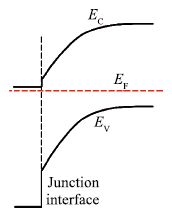
Fig. 1.
Symmetric n/p junction in equilibrium with $V =$ 0.
SEMICONDUCTOR PHYSICS
Abstract: The widely used deep level transient spectroscopy (DLTS) theory and data analysis usually assume that the defect level distribution is uniform through the depth of the depletion region of the n-p junction. In this work we introduce the concept of effective Fermi level of the steady state of semiconductor, by using which deep level transient spectroscopy depth profiling (DLTSDP) is proposed. Based on the relationship of its transition free energy level (TFEL) and the effective Fermi level, the rules of detectivity of the defect levels are listed. Computer simulation of DLTSDP is presented and compared with experimental data. The experimental DLTS data are compared with what the DLTSDP selection rules predicted. The agreement is satisfactory.
Keywords: Fermi level, deep level transient spectroscopy, Schottky junction
| [1] |
Lang D V. Deep-level transient spectroscopy: a new method to characterize traps in semiconductors. J Appl Phys, 1974, 45: 3023 doi: 10.1063/1.1663719
|
| [2] |
Henry C H, Lang D V. Nonradiative capture and recombination by multiphonon emission in GaAs and GaP. Phys Rev B, 1977, 15: 989 doi: 10.1103/PhysRevB.15.989
|
| [3] |
Orton J W, Blood P. The electrical characterization of semiconductors: measurement of minority carrier properties. Academic Press, 1990
|
| [4] |
Dhere R G, Zhang Y, Romero M J, et al. Investigation of junction properties of CdS/CdTe solar cells and their correlation to device properties. Proceedings of 33rd IEEE PVSC, San Diego, CA, May 2008: 1
|
| [5] |
Delahoy A E, Cheng Z, Chin K K. Evidence for CdTe1-xSx compound formation in CdTe solar cells from high-precision, temperature-dependent device measurements. Proceedings of 39th IEEE PVSC, Tampa, FL, June 2013: 1945
|
| [6] |
Delahoy A E, Cheng Z, Chin K K, et al. Modulation spectroscopy as a probe of surface electric field. Proceedings of 29th EU SEC, Amsterdam, September 2014: 1860
|
| [7] |
Chin K K. Transition Gibbs free energy level cross section and formulation of carrier SRH recombination rate. Journal of Semiconductors, 2013, 34(12): 122001 doi: 10.1088/1674-4926/34/12/122001
|
| [8] |
Wei S H, Zhang S B. Chemical trends of defect formation and doping limit in Ⅱ-VI semiconductors: the case of CdTe. Phys Rev B, 2002, 66: 15521
|
| [9] |
Ma J, Wei S H, Gessert T A, et al. Carrier density and compensation in semiconductors with multi dopants and multi transition energy levels: the case of Cu impurity in CdTe. Phys Rev B, 2011, 83: 245207 doi: 10.1103/PhysRevB.83.245207
|
| [10] |
Sze S. Physics of semiconductor devices. 2nd ed. New York: Wiley, 1981
|
| [11] |
Crandall R S. Meyer-Neldel rule in deep-level-transient-spectroscopy and its ramifications. Proceedings of MRS Symposium, San Francisco, April 2003: 79
|
| [12] |
Yelon A, Movaghar B, Crandall R S. Multi-excitation entropy: its role in thermodynamics and kinetics. Reports on Progress in Physics, 2006, 69: 1145 doi: 10.1088/0034-4885/69/4/R04
|
| [13] |
Chin K K. p-doping limit and donor compensation in CdTe polycrystalline thin film solar cells. Solar Energy Materials and Solar Cells, 2010, 94: 1627 doi: 10.1016/j.solmat.2010.05.006
|
| [14] |
Chin K K. Approximate graphical method for solving Fermi level and majority carrier density of semiconductors with multiple donors and multiple acceptors. Journal of Semiconductors, 2011, 32(6): 062001 doi: 10.1088/1674-4926/32/6/062001
|
| [15] |
Chin K K. Local charge neutrality condition, Fermi level, and majority carrier density of semiconductor with multiple localized multi-Level intrinsic/impurity Defects. Journal of Semiconductors, 2011, 32(11): 112001 doi: 10.1088/1674-4926/32/11/112001
|
| [16] |
Chin K K. Dual roles of doping and trapping of semiconductor defect levels and their ramification to thin film photovoltaics. J Appl Phys, 2012, 111: 104509 doi: 10.1063/1.4719046
|
| [17] |
Cao W. Analytical formulas for carrier density and Fermi energy in semiconductors with a tight-binding band. Journal of Semiconductors, 2015, 36(4): 042002 doi: 10.1088/1674-4926/36/4/042002
|
| [18] |
Chandra S T, Balamurugan N B, Bhuvaneswari M, et al. Analysis of charge density and Fermi level of AlInSb/InSb single-gate high electron mobility transistor. Journal of Semiconductors, 2015, 36(6): 064003 doi: 10.1088/1674-4926/36/6/064003
|
| [19] |
Cheng Z. Applications of defect level steady state occupation equation in CdTe solar cell. PhD Dissertation, NJIT, 2014
|
| [20] |
Cheng Z, Delahoy A E, Su Z, et al. Steady state minority carrier lifetime and defect level occupation in thin film CdTe solar cells. Thin Solid Films, 2014, 558: 391 doi: 10.1016/j.tsf.2014.02.070
|
| [21] |
Manual for AMPS-1D, the center for nanotechnology education and utilization, the Pennsylvania State University, 2003
|
| [22] |
Abulfotuh F A, Balcioglu A, Wangensteen T, et al. Study of the defect levels, electrooptics, and interface properties of polycrystalline CdTe and CdS thin films and their junction. Proceedings of 27th IEEE PVSC, Anaheim, CA, Sep 1997: 451
|
| [23] |
Balcioglu A, Ahrenkiel R K, Hasoon F. Deep-level impurities in CdTe/CdS thin-film solar cells. J Appl Phys, 2000, 88: 7175 doi: 10.1063/1.1326465
|
| [24] |
Wang Z, Li B, Zheng X, et al. Deep level transient spectroscopy investigation of deep levels in CdS/CdTe thin film solar cells with Te:Cu back contact. Chinese Physics B, 2010, 19: 027303 doi: 10.1088/1674-1056/19/2/027303
|
| [25] |
Li B, Feng L H, Wang Z, et al. Electronic properties and deep level transient spectroscopy of CdS/CdTe thin film solar cells. Chinese Physics B, 2011, 20: 037103 doi: 10.1088/1674-1056/20/3/037103
|
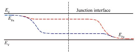
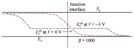
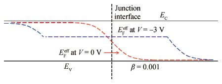
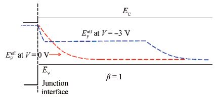
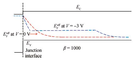
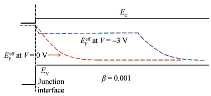
Table 1.
Dependence of

|
Table 2.
Majority carrier trap (HL,above

|
| [1] |
Lang D V. Deep-level transient spectroscopy: a new method to characterize traps in semiconductors. J Appl Phys, 1974, 45: 3023 doi: 10.1063/1.1663719
|
| [2] |
Henry C H, Lang D V. Nonradiative capture and recombination by multiphonon emission in GaAs and GaP. Phys Rev B, 1977, 15: 989 doi: 10.1103/PhysRevB.15.989
|
| [3] |
Orton J W, Blood P. The electrical characterization of semiconductors: measurement of minority carrier properties. Academic Press, 1990
|
| [4] |
Dhere R G, Zhang Y, Romero M J, et al. Investigation of junction properties of CdS/CdTe solar cells and their correlation to device properties. Proceedings of 33rd IEEE PVSC, San Diego, CA, May 2008: 1
|
| [5] |
Delahoy A E, Cheng Z, Chin K K. Evidence for CdTe1-xSx compound formation in CdTe solar cells from high-precision, temperature-dependent device measurements. Proceedings of 39th IEEE PVSC, Tampa, FL, June 2013: 1945
|
| [6] |
Delahoy A E, Cheng Z, Chin K K, et al. Modulation spectroscopy as a probe of surface electric field. Proceedings of 29th EU SEC, Amsterdam, September 2014: 1860
|
| [7] |
Chin K K. Transition Gibbs free energy level cross section and formulation of carrier SRH recombination rate. Journal of Semiconductors, 2013, 34(12): 122001 doi: 10.1088/1674-4926/34/12/122001
|
| [8] |
Wei S H, Zhang S B. Chemical trends of defect formation and doping limit in Ⅱ-VI semiconductors: the case of CdTe. Phys Rev B, 2002, 66: 15521
|
| [9] |
Ma J, Wei S H, Gessert T A, et al. Carrier density and compensation in semiconductors with multi dopants and multi transition energy levels: the case of Cu impurity in CdTe. Phys Rev B, 2011, 83: 245207 doi: 10.1103/PhysRevB.83.245207
|
| [10] |
Sze S. Physics of semiconductor devices. 2nd ed. New York: Wiley, 1981
|
| [11] |
Crandall R S. Meyer-Neldel rule in deep-level-transient-spectroscopy and its ramifications. Proceedings of MRS Symposium, San Francisco, April 2003: 79
|
| [12] |
Yelon A, Movaghar B, Crandall R S. Multi-excitation entropy: its role in thermodynamics and kinetics. Reports on Progress in Physics, 2006, 69: 1145 doi: 10.1088/0034-4885/69/4/R04
|
| [13] |
Chin K K. p-doping limit and donor compensation in CdTe polycrystalline thin film solar cells. Solar Energy Materials and Solar Cells, 2010, 94: 1627 doi: 10.1016/j.solmat.2010.05.006
|
| [14] |
Chin K K. Approximate graphical method for solving Fermi level and majority carrier density of semiconductors with multiple donors and multiple acceptors. Journal of Semiconductors, 2011, 32(6): 062001 doi: 10.1088/1674-4926/32/6/062001
|
| [15] |
Chin K K. Local charge neutrality condition, Fermi level, and majority carrier density of semiconductor with multiple localized multi-Level intrinsic/impurity Defects. Journal of Semiconductors, 2011, 32(11): 112001 doi: 10.1088/1674-4926/32/11/112001
|
| [16] |
Chin K K. Dual roles of doping and trapping of semiconductor defect levels and their ramification to thin film photovoltaics. J Appl Phys, 2012, 111: 104509 doi: 10.1063/1.4719046
|
| [17] |
Cao W. Analytical formulas for carrier density and Fermi energy in semiconductors with a tight-binding band. Journal of Semiconductors, 2015, 36(4): 042002 doi: 10.1088/1674-4926/36/4/042002
|
| [18] |
Chandra S T, Balamurugan N B, Bhuvaneswari M, et al. Analysis of charge density and Fermi level of AlInSb/InSb single-gate high electron mobility transistor. Journal of Semiconductors, 2015, 36(6): 064003 doi: 10.1088/1674-4926/36/6/064003
|
| [19] |
Cheng Z. Applications of defect level steady state occupation equation in CdTe solar cell. PhD Dissertation, NJIT, 2014
|
| [20] |
Cheng Z, Delahoy A E, Su Z, et al. Steady state minority carrier lifetime and defect level occupation in thin film CdTe solar cells. Thin Solid Films, 2014, 558: 391 doi: 10.1016/j.tsf.2014.02.070
|
| [21] |
Manual for AMPS-1D, the center for nanotechnology education and utilization, the Pennsylvania State University, 2003
|
| [22] |
Abulfotuh F A, Balcioglu A, Wangensteen T, et al. Study of the defect levels, electrooptics, and interface properties of polycrystalline CdTe and CdS thin films and their junction. Proceedings of 27th IEEE PVSC, Anaheim, CA, Sep 1997: 451
|
| [23] |
Balcioglu A, Ahrenkiel R K, Hasoon F. Deep-level impurities in CdTe/CdS thin-film solar cells. J Appl Phys, 2000, 88: 7175 doi: 10.1063/1.1326465
|
| [24] |
Wang Z, Li B, Zheng X, et al. Deep level transient spectroscopy investigation of deep levels in CdS/CdTe thin film solar cells with Te:Cu back contact. Chinese Physics B, 2010, 19: 027303 doi: 10.1088/1674-1056/19/2/027303
|
| [25] |
Li B, Feng L H, Wang Z, et al. Electronic properties and deep level transient spectroscopy of CdS/CdTe thin film solar cells. Chinese Physics B, 2011, 20: 037103 doi: 10.1088/1674-1056/20/3/037103
|


Article views: 4095 Times PDF downloads: 45 Times Cited by: 0 Times
Received: 07 October 2015 Revised: 13 April 2016 Online: Published: 01 September 2016
| Citation: |
Ken K. Chin, Zimeng Cheng. Semiconductor steady state defect effective Fermi level and deep level transient spectroscopy depth profiling[J]. Journal of Semiconductors, 2016, 37(9): 092003. doi: 10.1088/1674-4926/37/9/092003
****
K. K. Chin, Z M Cheng. Semiconductor steady state defect effective Fermi level and deep level transient spectroscopy depth profiling[J]. J. Semicond., 2016, 37(9): 092003. doi: 10.1088/1674-4926/37/9/092003.

|
| [1] |
Lang D V. Deep-level transient spectroscopy: a new method to characterize traps in semiconductors. J Appl Phys, 1974, 45: 3023 doi: 10.1063/1.1663719
|
| [2] |
Henry C H, Lang D V. Nonradiative capture and recombination by multiphonon emission in GaAs and GaP. Phys Rev B, 1977, 15: 989 doi: 10.1103/PhysRevB.15.989
|
| [3] |
Orton J W, Blood P. The electrical characterization of semiconductors: measurement of minority carrier properties. Academic Press, 1990
|
| [4] |
Dhere R G, Zhang Y, Romero M J, et al. Investigation of junction properties of CdS/CdTe solar cells and their correlation to device properties. Proceedings of 33rd IEEE PVSC, San Diego, CA, May 2008: 1
|
| [5] |
Delahoy A E, Cheng Z, Chin K K. Evidence for CdTe1-xSx compound formation in CdTe solar cells from high-precision, temperature-dependent device measurements. Proceedings of 39th IEEE PVSC, Tampa, FL, June 2013: 1945
|
| [6] |
Delahoy A E, Cheng Z, Chin K K, et al. Modulation spectroscopy as a probe of surface electric field. Proceedings of 29th EU SEC, Amsterdam, September 2014: 1860
|
| [7] |
Chin K K. Transition Gibbs free energy level cross section and formulation of carrier SRH recombination rate. Journal of Semiconductors, 2013, 34(12): 122001 doi: 10.1088/1674-4926/34/12/122001
|
| [8] |
Wei S H, Zhang S B. Chemical trends of defect formation and doping limit in Ⅱ-VI semiconductors: the case of CdTe. Phys Rev B, 2002, 66: 15521
|
| [9] |
Ma J, Wei S H, Gessert T A, et al. Carrier density and compensation in semiconductors with multi dopants and multi transition energy levels: the case of Cu impurity in CdTe. Phys Rev B, 2011, 83: 245207 doi: 10.1103/PhysRevB.83.245207
|
| [10] |
Sze S. Physics of semiconductor devices. 2nd ed. New York: Wiley, 1981
|
| [11] |
Crandall R S. Meyer-Neldel rule in deep-level-transient-spectroscopy and its ramifications. Proceedings of MRS Symposium, San Francisco, April 2003: 79
|
| [12] |
Yelon A, Movaghar B, Crandall R S. Multi-excitation entropy: its role in thermodynamics and kinetics. Reports on Progress in Physics, 2006, 69: 1145 doi: 10.1088/0034-4885/69/4/R04
|
| [13] |
Chin K K. p-doping limit and donor compensation in CdTe polycrystalline thin film solar cells. Solar Energy Materials and Solar Cells, 2010, 94: 1627 doi: 10.1016/j.solmat.2010.05.006
|
| [14] |
Chin K K. Approximate graphical method for solving Fermi level and majority carrier density of semiconductors with multiple donors and multiple acceptors. Journal of Semiconductors, 2011, 32(6): 062001 doi: 10.1088/1674-4926/32/6/062001
|
| [15] |
Chin K K. Local charge neutrality condition, Fermi level, and majority carrier density of semiconductor with multiple localized multi-Level intrinsic/impurity Defects. Journal of Semiconductors, 2011, 32(11): 112001 doi: 10.1088/1674-4926/32/11/112001
|
| [16] |
Chin K K. Dual roles of doping and trapping of semiconductor defect levels and their ramification to thin film photovoltaics. J Appl Phys, 2012, 111: 104509 doi: 10.1063/1.4719046
|
| [17] |
Cao W. Analytical formulas for carrier density and Fermi energy in semiconductors with a tight-binding band. Journal of Semiconductors, 2015, 36(4): 042002 doi: 10.1088/1674-4926/36/4/042002
|
| [18] |
Chandra S T, Balamurugan N B, Bhuvaneswari M, et al. Analysis of charge density and Fermi level of AlInSb/InSb single-gate high electron mobility transistor. Journal of Semiconductors, 2015, 36(6): 064003 doi: 10.1088/1674-4926/36/6/064003
|
| [19] |
Cheng Z. Applications of defect level steady state occupation equation in CdTe solar cell. PhD Dissertation, NJIT, 2014
|
| [20] |
Cheng Z, Delahoy A E, Su Z, et al. Steady state minority carrier lifetime and defect level occupation in thin film CdTe solar cells. Thin Solid Films, 2014, 558: 391 doi: 10.1016/j.tsf.2014.02.070
|
| [21] |
Manual for AMPS-1D, the center for nanotechnology education and utilization, the Pennsylvania State University, 2003
|
| [22] |
Abulfotuh F A, Balcioglu A, Wangensteen T, et al. Study of the defect levels, electrooptics, and interface properties of polycrystalline CdTe and CdS thin films and their junction. Proceedings of 27th IEEE PVSC, Anaheim, CA, Sep 1997: 451
|
| [23] |
Balcioglu A, Ahrenkiel R K, Hasoon F. Deep-level impurities in CdTe/CdS thin-film solar cells. J Appl Phys, 2000, 88: 7175 doi: 10.1063/1.1326465
|
| [24] |
Wang Z, Li B, Zheng X, et al. Deep level transient spectroscopy investigation of deep levels in CdS/CdTe thin film solar cells with Te:Cu back contact. Chinese Physics B, 2010, 19: 027303 doi: 10.1088/1674-1056/19/2/027303
|
| [25] |
Li B, Feng L H, Wang Z, et al. Electronic properties and deep level transient spectroscopy of CdS/CdTe thin film solar cells. Chinese Physics B, 2011, 20: 037103 doi: 10.1088/1674-1056/20/3/037103
|

 WeChat ID
Journal of Semiconductors © 2017 All Rights Reserved 京ICP备05085259号-2

 DownLoad: