


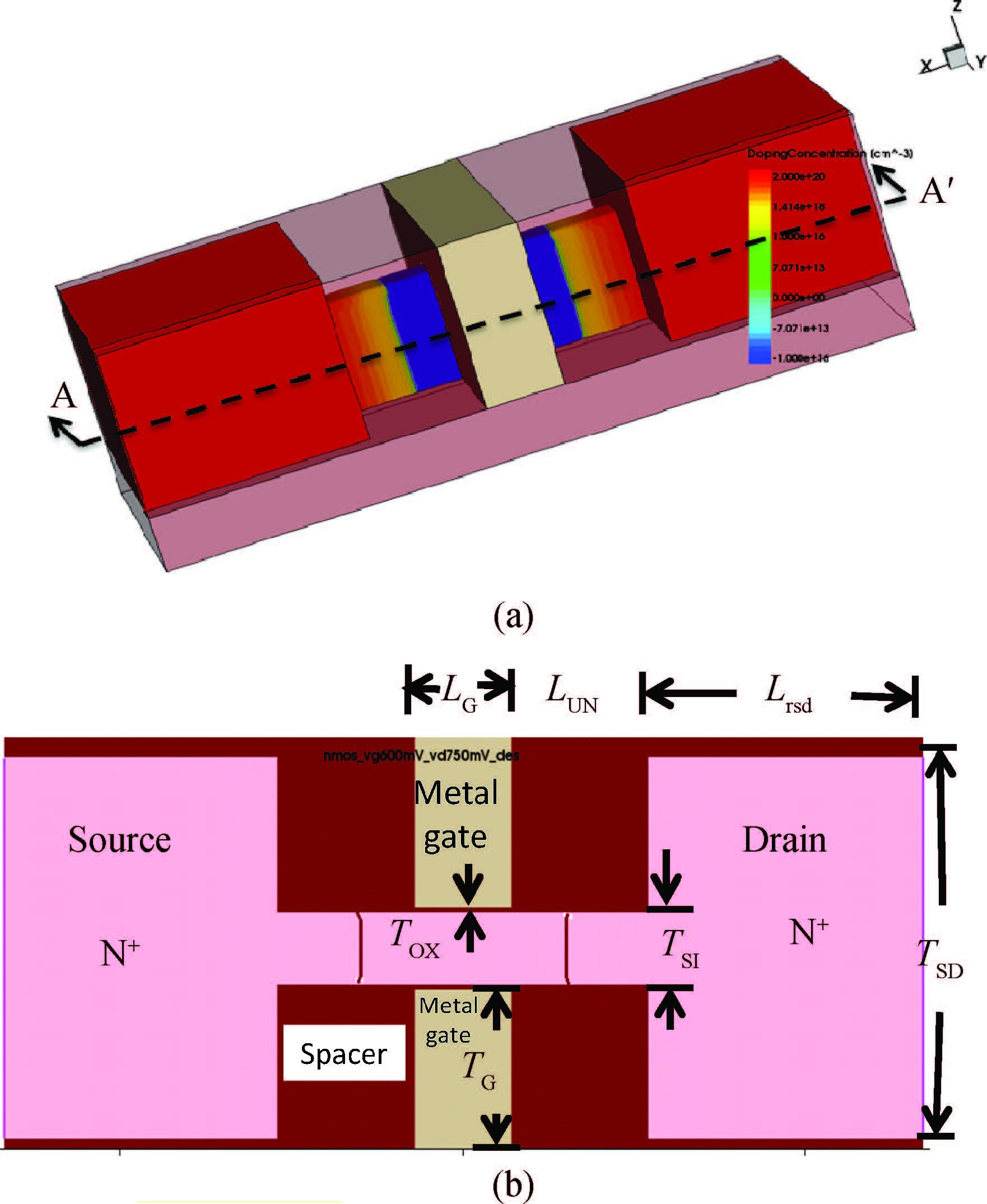
Fig. 1.
(Color online) (a) 3-D structure and (b) 2-D cross section along A-A' axis of an underlap n-FinFET considered for the potential analysis simulated with TCAD LG=16 nm,H FIN= 30 nm,T Si =8 nm,T SD=20 nm,T OX=1.7 nm.
SEMICONDUCTOR DEVICES
Abstract: This paper delineates the effect of nonplanar structure of FinFETs on noise performance. We demonstrate the thermal noise analytical model that has been inferred by taking into account the presence of an additional inverted region in the extended (underlap) S/D region due to finite gate electrode thickness. Noise investigation includes the effects of source drain resistances which become significant as channel length becomes shorter. In this paper, we evaluate the additional noise caused by three dimensional (3-D) structure of the single fin device and then extended analysis of the multi-fin and multi-fingers structure. The addition of fringe field increases its minimum noise figure and noise resistance of approximately 1 dB and 100 Ω respectively and optimum admittance increases to 5.45 mω at 20 GHz for a device operating under saturation region. Hence, our transformed model plays a significant function in evaluation of accurate noise performance at circuit level.
Keywords: FinFET, thermal noise, model
| [1] | |
| [2] |
Guo Yiluan, Wang Guilei, Zhao Chao, et al. Simulation and characterization of stress in FinFETs using novel LKMC and nanobeam diffraction methods. Journal of Semiconductors, 2015, 36(8): 086001 doi: 10.1088/1674-4926/36/8/086001
|
| [3] |
Scholten A J, Tiemeijer L F, van Langevelde R, et al. Noise modeling for RF CMOS circuit simulation. IEEE Trans Electron Devices, 2003, 50(3): 618 doi: 10.1109/TED.2003.810480
|
| [4] |
Scholten A J, Smit G D J, Pijpere R M T, et al. FinFET compact modelling for analogue and RF applications. IEEE International Electron Devices Meeting, 2010, 2: 8.4.1 http://cn.bing.com/academic/profile?id=2149741487&encoded=0&v=paper_preview&mkt=zh-cn
|
| [5] |
Raskin J, Pailloncy G, Lederer D, et al. High-frequency noise performance of 60-nm gate-length FinFETs. IEEE Trans Electron Devices, 2008, 55(10): 2718 doi: 10.1109/TED.2008.2003097
|
| [6] |
Wei C, Xiong Y Z, Zhou X. Investigation of low-frequency noise in n-channel FinFETs from weak to strong inversion. IEEE Electron Devices, 2009, 56(11): 2800 doi: 10.1109/TED.2009.2030972
|
| [7] |
vKlaassen F M, Prins J. Thermal noise of MOS transistors. Philips Res RTep, 1967, 22: 505 http://cn.bing.com/academic/profile?id=138059704&encoded=0&v=paper_preview&mkt=zh-cn
|
| [8] |
Paasschens J C J, Scholten A J, van Langevelde R. Generalizations of the Klaassen-Prins equation for calculating the noise of semiconductor devices. IEEE Trans Electron Devices, 2005, 52(11): 2463 doi: 10.1109/TED.2005.857189
|
| [9] |
Shoji M. Analysis of high-frequency thermal noise of enhancement mode MOS field-effect transistors. IEEE Trans Electron Devices, 1966, ED-13(6): 520 doi: 10.1109/T-ED.1966.15724
|
| [10] |
Knoblinger G, Fulde M, Siprak D, et al. Evaluation of FinFET RF building blocks. Proc IEEE International SOI Conference, 2007: 39 http://cn.bing.com/academic/profile?id=2027795658&encoded=0&v=paper_preview&mkt=zh-cn
|
| [11] |
Li Z. Compact channel noise models for MOSFETs, deep-submicron. IEEE Trans Electron Devices, 2009, 56(6): 1300 doi: 10.1109/TED.2009.2018160
|
| [12] |
Bruncke W C. Noise measurements in field-effect transistors. Proceedings of IEEE (Correspondence), 1963, 51: 378 doi: 10.1109/PROC.1963.1795
|
| [13] |
Lu D. Compact models for future generation CMOS. PhD Dissertation, Electrical Engineering and Computer Sciences, University of California, Berkeley, 2011
|
| [14] |
Lu N, Kotecha P M, Wachnik R A. Modeling of resistance in FinFET local interconnect. IEEE Circuits and Systems Society, 2015, 62(8): 1899 http://cn.bing.com/academic/profile?id=1537227151&encoded=0&v=paper_preview&mkt=zh-cn
|
| [15] |
Huang X, Lee W C, Kuo C, et al. Sub-50 nm p-channel FinFET. IEEE Trans Electron Devices, 2001, 48(5): 880 doi: 10.1109/16.918235
|
| [16] |
Chen C H, Deen M J. High frequency noise of MOSFETs I modeling. Solid State Electron, 1998, 42(11): 2069 doi: 10.1016/S0038-1101(98)00192-0
|
| [17] |
Arora N. MOSFET modelling for VLSI simulation theory and practice. World Scientific, 2007
|
| [18] |
Laìzaro A, Nae B, Iñiguez B, et al. A compact quantum model for fin-shaped field effect transistors valid from dc to high frequency and noise simulations. J Appl Phys, 2008, 103(8): 084507 doi: 10.1063/1.2907720
|
| [19] |
Mudanai S, Roy A. Capacitance compact model for ultrathin low-electron-effective-mass materials. IEEE Trans Electron Devices, 2011, 58(12): 4204 doi: 10.1109/TED.2011.2168529
|
| [20] |
Shrivastava R. Fitzpatrick K. A simple model for the overlap capacitance of a VLSI MOS device. IEEE Trans Electron Devices, 1982, ED-29(12):1870 http://cn.bing.com/academic/profile?id=1976988595&encoded=0&v=paper_preview&mkt=zh-cn
|
| [21] |
Jagadesh M K, Gupta S K, Venkataraman V. Compact modeling of the effects of parasitic internal fringe capacitance on the threshold voltage of high-k gate-dielectric nanoscale SOI MOSFETs. IEEE Trans Electron Devices, 2006, 53(4): 706 doi: 10.1109/TED.2006.870424
|
| [22] |
Roy A S, Enz C C, Sallese J M. Noise modeling methodologies in the presence of mobility degradation and their equivalence. IEEE Trans Electron Devices, 2006, 53(2): 348 doi: 10.1109/TED.2005.862703
|
| [23] |
Mukherjee C, Maiti C K. Channel thermal noise modeling and high frequency noise parameters of tri-gate FinFETs. 20th IEEE International Symposium on the Physical and Failure Analysis of Integrated Circuits (IPFA), 2013, 2(5): 732 http://cn.bing.com/academic/profile?id=2021830009&encoded=0&v=paper_preview&mkt=zh-cn
|
| [24] |
Xu Miao, Yin Huaxiang, Zhu Huilong, et al. Device parameter optimization for sub-20 nm node HK/MG-last bulk FinFETs. Journal of Semiconductors, 2015, 36(4): 044007 doi: 10.1088/1674-4926/36/4/044007
|
| [25] |
Suresh D, Nagarajan K K, Srinivasan R. The impact of process variations on input impedance and mitigation using a circuit technique in FinFET-based LNA. Journal of Semiconductors, 2015, 36(4): 045002 doi: 10.1088/1674-4926/36/4/045002
|
| [26] |
Wu Weikang, An Xia, Jiang Xiaobo, et al. Line-edge roughness induced single event transient variation in SOI FinFETs. Journal of Semiconductors, 2015, 36(11): 114001 doi: 10.1088/1674-4926/36/11/114001
|
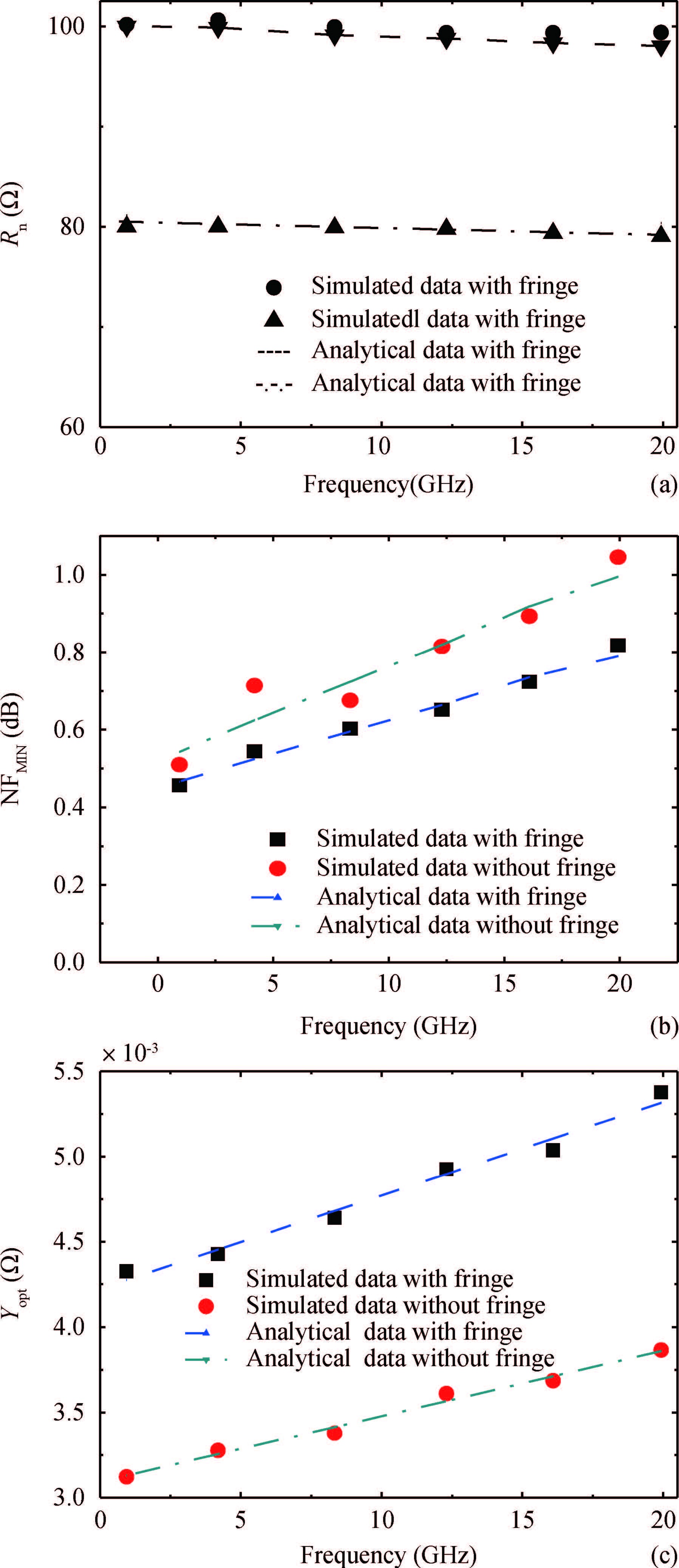
Table 1. Device dimensions.

|
Table 2. Extracted small signal equivalent circuit parameter versus number of fingers and RF noise parameter at 10 GHz for 16 nm gate length finFET,number of fins = 5/finger.

|
| [1] | |
| [2] |
Guo Yiluan, Wang Guilei, Zhao Chao, et al. Simulation and characterization of stress in FinFETs using novel LKMC and nanobeam diffraction methods. Journal of Semiconductors, 2015, 36(8): 086001 doi: 10.1088/1674-4926/36/8/086001
|
| [3] |
Scholten A J, Tiemeijer L F, van Langevelde R, et al. Noise modeling for RF CMOS circuit simulation. IEEE Trans Electron Devices, 2003, 50(3): 618 doi: 10.1109/TED.2003.810480
|
| [4] |
Scholten A J, Smit G D J, Pijpere R M T, et al. FinFET compact modelling for analogue and RF applications. IEEE International Electron Devices Meeting, 2010, 2: 8.4.1 http://cn.bing.com/academic/profile?id=2149741487&encoded=0&v=paper_preview&mkt=zh-cn
|
| [5] |
Raskin J, Pailloncy G, Lederer D, et al. High-frequency noise performance of 60-nm gate-length FinFETs. IEEE Trans Electron Devices, 2008, 55(10): 2718 doi: 10.1109/TED.2008.2003097
|
| [6] |
Wei C, Xiong Y Z, Zhou X. Investigation of low-frequency noise in n-channel FinFETs from weak to strong inversion. IEEE Electron Devices, 2009, 56(11): 2800 doi: 10.1109/TED.2009.2030972
|
| [7] |
vKlaassen F M, Prins J. Thermal noise of MOS transistors. Philips Res RTep, 1967, 22: 505 http://cn.bing.com/academic/profile?id=138059704&encoded=0&v=paper_preview&mkt=zh-cn
|
| [8] |
Paasschens J C J, Scholten A J, van Langevelde R. Generalizations of the Klaassen-Prins equation for calculating the noise of semiconductor devices. IEEE Trans Electron Devices, 2005, 52(11): 2463 doi: 10.1109/TED.2005.857189
|
| [9] |
Shoji M. Analysis of high-frequency thermal noise of enhancement mode MOS field-effect transistors. IEEE Trans Electron Devices, 1966, ED-13(6): 520 doi: 10.1109/T-ED.1966.15724
|
| [10] |
Knoblinger G, Fulde M, Siprak D, et al. Evaluation of FinFET RF building blocks. Proc IEEE International SOI Conference, 2007: 39 http://cn.bing.com/academic/profile?id=2027795658&encoded=0&v=paper_preview&mkt=zh-cn
|
| [11] |
Li Z. Compact channel noise models for MOSFETs, deep-submicron. IEEE Trans Electron Devices, 2009, 56(6): 1300 doi: 10.1109/TED.2009.2018160
|
| [12] |
Bruncke W C. Noise measurements in field-effect transistors. Proceedings of IEEE (Correspondence), 1963, 51: 378 doi: 10.1109/PROC.1963.1795
|
| [13] |
Lu D. Compact models for future generation CMOS. PhD Dissertation, Electrical Engineering and Computer Sciences, University of California, Berkeley, 2011
|
| [14] |
Lu N, Kotecha P M, Wachnik R A. Modeling of resistance in FinFET local interconnect. IEEE Circuits and Systems Society, 2015, 62(8): 1899 http://cn.bing.com/academic/profile?id=1537227151&encoded=0&v=paper_preview&mkt=zh-cn
|
| [15] |
Huang X, Lee W C, Kuo C, et al. Sub-50 nm p-channel FinFET. IEEE Trans Electron Devices, 2001, 48(5): 880 doi: 10.1109/16.918235
|
| [16] |
Chen C H, Deen M J. High frequency noise of MOSFETs I modeling. Solid State Electron, 1998, 42(11): 2069 doi: 10.1016/S0038-1101(98)00192-0
|
| [17] |
Arora N. MOSFET modelling for VLSI simulation theory and practice. World Scientific, 2007
|
| [18] |
Laìzaro A, Nae B, Iñiguez B, et al. A compact quantum model for fin-shaped field effect transistors valid from dc to high frequency and noise simulations. J Appl Phys, 2008, 103(8): 084507 doi: 10.1063/1.2907720
|
| [19] |
Mudanai S, Roy A. Capacitance compact model for ultrathin low-electron-effective-mass materials. IEEE Trans Electron Devices, 2011, 58(12): 4204 doi: 10.1109/TED.2011.2168529
|
| [20] |
Shrivastava R. Fitzpatrick K. A simple model for the overlap capacitance of a VLSI MOS device. IEEE Trans Electron Devices, 1982, ED-29(12):1870 http://cn.bing.com/academic/profile?id=1976988595&encoded=0&v=paper_preview&mkt=zh-cn
|
| [21] |
Jagadesh M K, Gupta S K, Venkataraman V. Compact modeling of the effects of parasitic internal fringe capacitance on the threshold voltage of high-k gate-dielectric nanoscale SOI MOSFETs. IEEE Trans Electron Devices, 2006, 53(4): 706 doi: 10.1109/TED.2006.870424
|
| [22] |
Roy A S, Enz C C, Sallese J M. Noise modeling methodologies in the presence of mobility degradation and their equivalence. IEEE Trans Electron Devices, 2006, 53(2): 348 doi: 10.1109/TED.2005.862703
|
| [23] |
Mukherjee C, Maiti C K. Channel thermal noise modeling and high frequency noise parameters of tri-gate FinFETs. 20th IEEE International Symposium on the Physical and Failure Analysis of Integrated Circuits (IPFA), 2013, 2(5): 732 http://cn.bing.com/academic/profile?id=2021830009&encoded=0&v=paper_preview&mkt=zh-cn
|
| [24] |
Xu Miao, Yin Huaxiang, Zhu Huilong, et al. Device parameter optimization for sub-20 nm node HK/MG-last bulk FinFETs. Journal of Semiconductors, 2015, 36(4): 044007 doi: 10.1088/1674-4926/36/4/044007
|
| [25] |
Suresh D, Nagarajan K K, Srinivasan R. The impact of process variations on input impedance and mitigation using a circuit technique in FinFET-based LNA. Journal of Semiconductors, 2015, 36(4): 045002 doi: 10.1088/1674-4926/36/4/045002
|
| [26] |
Wu Weikang, An Xia, Jiang Xiaobo, et al. Line-edge roughness induced single event transient variation in SOI FinFETs. Journal of Semiconductors, 2015, 36(11): 114001 doi: 10.1088/1674-4926/36/11/114001
|


Article views: 4029 Times PDF downloads: 55 Times Cited by: 0 Times
Received: 14 January 2016 Revised: 08 March 2016 Online: Published: 01 September 2016
| Citation: |
Savitesh Madhulika Sharma, S. Dasgupta, M. V. Kartikeyan. A transformed analytical model for thermal noise of FinFET based on fringing field approximation[J]. Journal of Semiconductors, 2016, 37(9): 094001. doi: 10.1088/1674-4926/37/9/094001
****
S M Sharma, S. Dasgupta, M. V. Kartikeyan. A transformed analytical model for thermal noise of FinFET based on fringing field approximation[J]. J. Semicond., 2016, 37(9): 094001. doi: 10.1088/1674-4926/37/9/094001.

|
| [1] | |
| [2] |
Guo Yiluan, Wang Guilei, Zhao Chao, et al. Simulation and characterization of stress in FinFETs using novel LKMC and nanobeam diffraction methods. Journal of Semiconductors, 2015, 36(8): 086001 doi: 10.1088/1674-4926/36/8/086001
|
| [3] |
Scholten A J, Tiemeijer L F, van Langevelde R, et al. Noise modeling for RF CMOS circuit simulation. IEEE Trans Electron Devices, 2003, 50(3): 618 doi: 10.1109/TED.2003.810480
|
| [4] |
Scholten A J, Smit G D J, Pijpere R M T, et al. FinFET compact modelling for analogue and RF applications. IEEE International Electron Devices Meeting, 2010, 2: 8.4.1 http://cn.bing.com/academic/profile?id=2149741487&encoded=0&v=paper_preview&mkt=zh-cn
|
| [5] |
Raskin J, Pailloncy G, Lederer D, et al. High-frequency noise performance of 60-nm gate-length FinFETs. IEEE Trans Electron Devices, 2008, 55(10): 2718 doi: 10.1109/TED.2008.2003097
|
| [6] |
Wei C, Xiong Y Z, Zhou X. Investigation of low-frequency noise in n-channel FinFETs from weak to strong inversion. IEEE Electron Devices, 2009, 56(11): 2800 doi: 10.1109/TED.2009.2030972
|
| [7] |
vKlaassen F M, Prins J. Thermal noise of MOS transistors. Philips Res RTep, 1967, 22: 505 http://cn.bing.com/academic/profile?id=138059704&encoded=0&v=paper_preview&mkt=zh-cn
|
| [8] |
Paasschens J C J, Scholten A J, van Langevelde R. Generalizations of the Klaassen-Prins equation for calculating the noise of semiconductor devices. IEEE Trans Electron Devices, 2005, 52(11): 2463 doi: 10.1109/TED.2005.857189
|
| [9] |
Shoji M. Analysis of high-frequency thermal noise of enhancement mode MOS field-effect transistors. IEEE Trans Electron Devices, 1966, ED-13(6): 520 doi: 10.1109/T-ED.1966.15724
|
| [10] |
Knoblinger G, Fulde M, Siprak D, et al. Evaluation of FinFET RF building blocks. Proc IEEE International SOI Conference, 2007: 39 http://cn.bing.com/academic/profile?id=2027795658&encoded=0&v=paper_preview&mkt=zh-cn
|
| [11] |
Li Z. Compact channel noise models for MOSFETs, deep-submicron. IEEE Trans Electron Devices, 2009, 56(6): 1300 doi: 10.1109/TED.2009.2018160
|
| [12] |
Bruncke W C. Noise measurements in field-effect transistors. Proceedings of IEEE (Correspondence), 1963, 51: 378 doi: 10.1109/PROC.1963.1795
|
| [13] |
Lu D. Compact models for future generation CMOS. PhD Dissertation, Electrical Engineering and Computer Sciences, University of California, Berkeley, 2011
|
| [14] |
Lu N, Kotecha P M, Wachnik R A. Modeling of resistance in FinFET local interconnect. IEEE Circuits and Systems Society, 2015, 62(8): 1899 http://cn.bing.com/academic/profile?id=1537227151&encoded=0&v=paper_preview&mkt=zh-cn
|
| [15] |
Huang X, Lee W C, Kuo C, et al. Sub-50 nm p-channel FinFET. IEEE Trans Electron Devices, 2001, 48(5): 880 doi: 10.1109/16.918235
|
| [16] |
Chen C H, Deen M J. High frequency noise of MOSFETs I modeling. Solid State Electron, 1998, 42(11): 2069 doi: 10.1016/S0038-1101(98)00192-0
|
| [17] |
Arora N. MOSFET modelling for VLSI simulation theory and practice. World Scientific, 2007
|
| [18] |
Laìzaro A, Nae B, Iñiguez B, et al. A compact quantum model for fin-shaped field effect transistors valid from dc to high frequency and noise simulations. J Appl Phys, 2008, 103(8): 084507 doi: 10.1063/1.2907720
|
| [19] |
Mudanai S, Roy A. Capacitance compact model for ultrathin low-electron-effective-mass materials. IEEE Trans Electron Devices, 2011, 58(12): 4204 doi: 10.1109/TED.2011.2168529
|
| [20] |
Shrivastava R. Fitzpatrick K. A simple model for the overlap capacitance of a VLSI MOS device. IEEE Trans Electron Devices, 1982, ED-29(12):1870 http://cn.bing.com/academic/profile?id=1976988595&encoded=0&v=paper_preview&mkt=zh-cn
|
| [21] |
Jagadesh M K, Gupta S K, Venkataraman V. Compact modeling of the effects of parasitic internal fringe capacitance on the threshold voltage of high-k gate-dielectric nanoscale SOI MOSFETs. IEEE Trans Electron Devices, 2006, 53(4): 706 doi: 10.1109/TED.2006.870424
|
| [22] |
Roy A S, Enz C C, Sallese J M. Noise modeling methodologies in the presence of mobility degradation and their equivalence. IEEE Trans Electron Devices, 2006, 53(2): 348 doi: 10.1109/TED.2005.862703
|
| [23] |
Mukherjee C, Maiti C K. Channel thermal noise modeling and high frequency noise parameters of tri-gate FinFETs. 20th IEEE International Symposium on the Physical and Failure Analysis of Integrated Circuits (IPFA), 2013, 2(5): 732 http://cn.bing.com/academic/profile?id=2021830009&encoded=0&v=paper_preview&mkt=zh-cn
|
| [24] |
Xu Miao, Yin Huaxiang, Zhu Huilong, et al. Device parameter optimization for sub-20 nm node HK/MG-last bulk FinFETs. Journal of Semiconductors, 2015, 36(4): 044007 doi: 10.1088/1674-4926/36/4/044007
|
| [25] |
Suresh D, Nagarajan K K, Srinivasan R. The impact of process variations on input impedance and mitigation using a circuit technique in FinFET-based LNA. Journal of Semiconductors, 2015, 36(4): 045002 doi: 10.1088/1674-4926/36/4/045002
|
| [26] |
Wu Weikang, An Xia, Jiang Xiaobo, et al. Line-edge roughness induced single event transient variation in SOI FinFETs. Journal of Semiconductors, 2015, 36(11): 114001 doi: 10.1088/1674-4926/36/11/114001
|

 WeChat ID
Journal of Semiconductors © 2017 All Rights Reserved 京ICP备05085259号-2

 DownLoad:

