


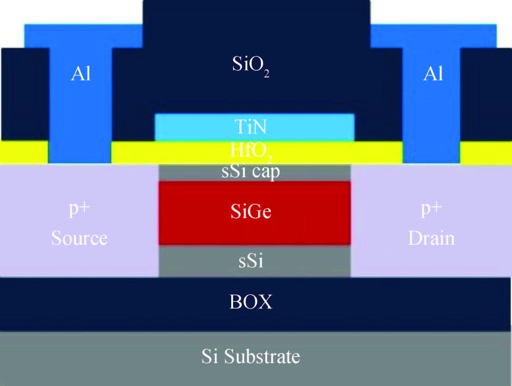
Fig. 1.
(Color online) Schematic view of sSi/Si0.5Ge0.5/sSOI QW p-MOSFET's cross-section.
SEMICONDUCTOR DEVICES
Jiao Wen1, 2, Qiang Liu1, 2, Chang Liu2, Yize Wang2, Bo Zhang2, Zhongying Xue2, Zengfeng Di2, Wenjie Yu2, and Qingtai Zhao3
Corresponding author: Wenjie Yu, casan@mail.sim.ac.cn
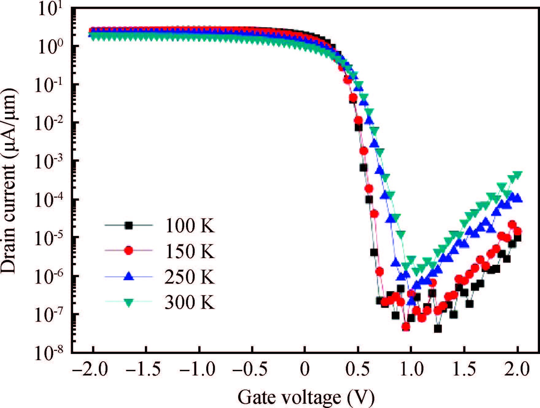
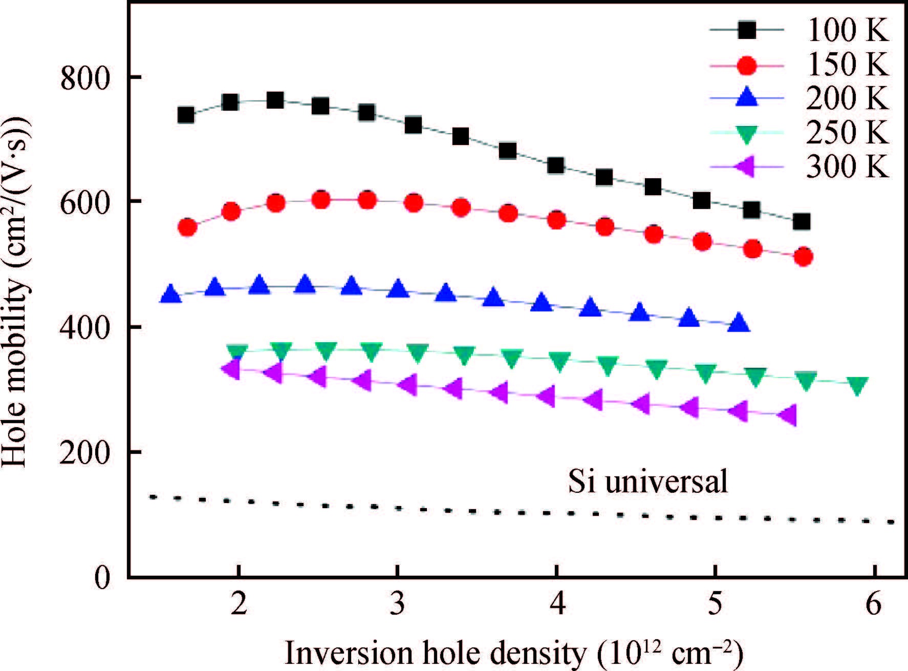
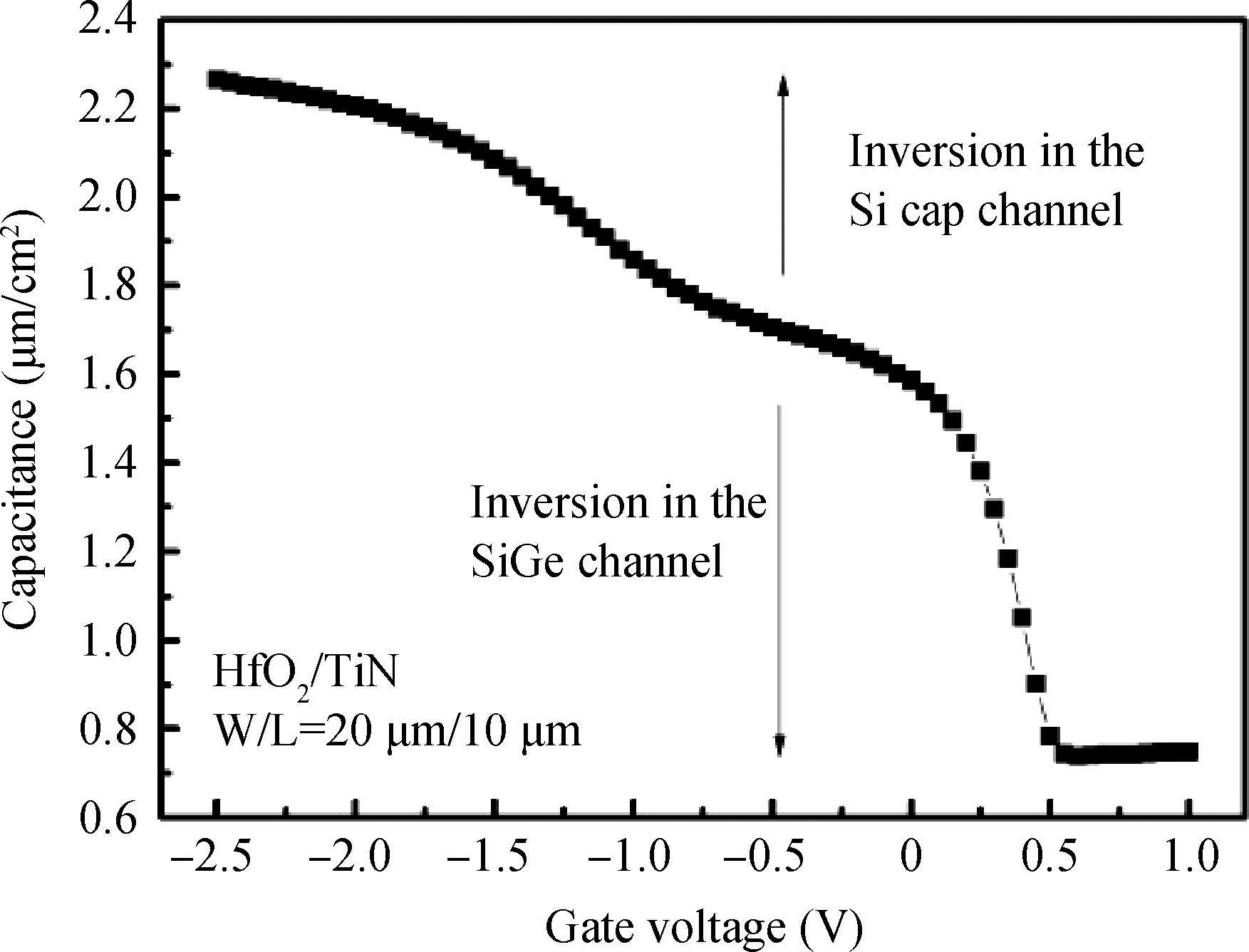
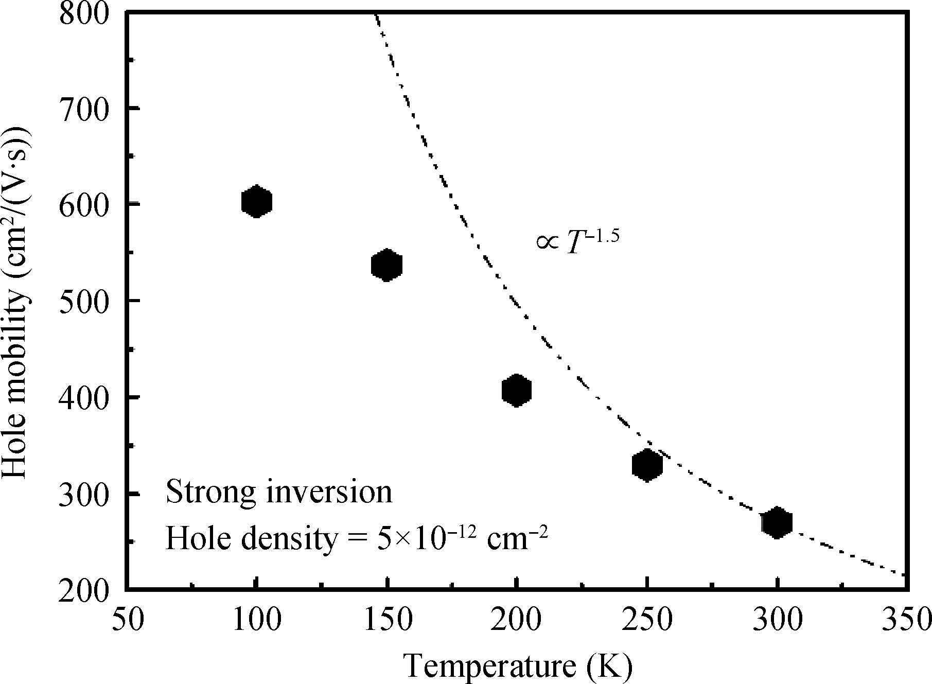
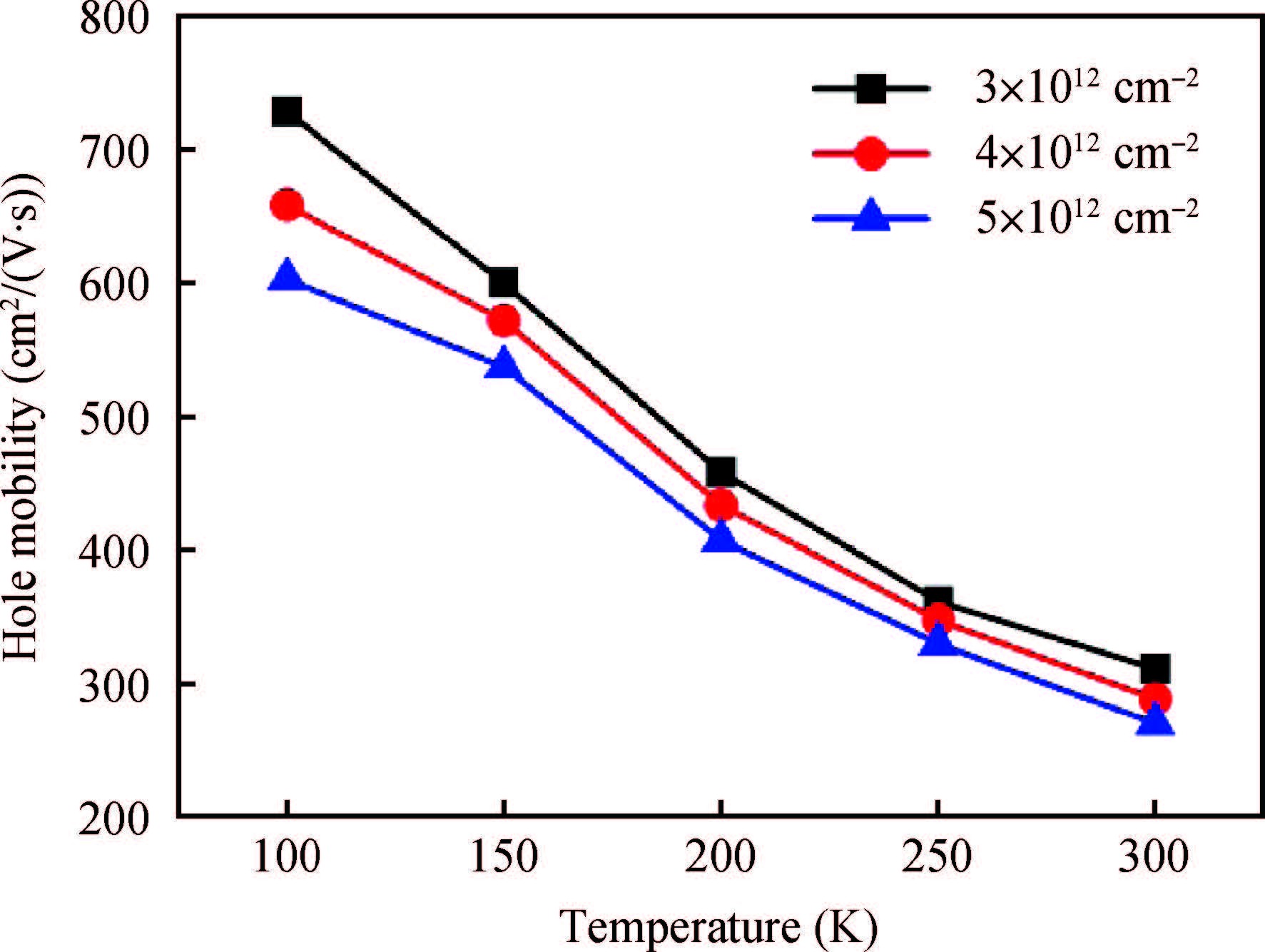
Abstract: sSi/Si0.5Ge0.5/sSOI quantum-well (QW) p-MOSFETs with HfO2/TiN gate stack were fabricated and characterized. According to the low temperature experimental results, carrier mobility of the strained Si0.5Ge0.5 QW p-MOSFET was mainly governed by phonon scattering from 300 to 150 K and Coulomb scattering below 150 K, respectively. Coulomb scattering was intensified by the accumulated inversion charges in the Si cap layer of this Si/SiGe heterostructure, which led to a degradation of carrier mobility in the SiGe channel, especially at low temperature.
Keywords: SiGe, quantum-well, hole mobility, Coulomb scattering
| [1] |
Hill R J W, Moran D A J, Li X, et al. Enhancement-mode GaAs MOSFETs with an In0.3Ga0.7As channel, a mobility of over 5000 cm2/(V· s), and transconductance of over 475μS/μm. IEEE Electron Device Lett, 2007, 28(12): 1080 doi: 10.1109/LED.2007.910009
|
| [2] |
Lee M L, Fitzgerald E A, Bulsara M T, et al. Strained Si, SiGe, and Ge channels for high-mobility metal-oxide-semiconductor field-effect transistors. J Appl Phys, 2005, 97(1): 011101 doi: 10.1063/1.1819976
|
| [3] |
Takagi S, Tezuka T, Irisawa T, et al. Device structures and carrier transport properties of advanced CMOS using high mobility channels. Solid-State Electron, 2007, 51(4): 526 doi: 10.1016/j.sse.2007.02.017
|
| [4] |
Cui W, Tang Z H, Tan K Z, et al. A strained Si-channel NMOSFET with low field mobility enhancement of about 140% using a SiGe virtual substrate. Journal of Semiconductors, 2012, 33(9): 094005 doi: 10.1088/1674-4926/33/9/094005
|
| [5] |
Chaudhry A, Roy J N, Garima J. Nanoscale strained-Si MOSFET physics and modeling approaches: a review. Journal of Semiconductors, 2010, 31(10): 104001 doi: 10.1088/1674-4926/31/10/104001
|
| [6] |
Von Haartman M, Malm B G, Ostling M. Comprehensive study on low-frequency noise and mobility in Si and SiGe PMOSFETS with high-k gate dielectrics and TiN gate. IEEE Trans Electron Devices, 2006, 53(4): 836 doi: 10.1109/TED.2006.870276
|
| [7] |
Gomez L, Hashemi P, Hoyt J L. Enhanced hole transport in short-channel strained-SiGe p-MOSFETs. IEEE Trans Electron Devices, 2009, 56(11): 2644 doi: 10.1109/TED.2009.2031043
|
| [8] |
Loo R, Sorada H, Inoue A, et al. Selective epitaxial Si/SiGe growth for VT shift adjustment in high-κ pMOS devices. Semicond Sci Technol, 2007, 22(1): 110 doi: 10.1088/0268-1242/22/1/S26
|
| [9] |
Fischetti M, Laux S. Band structure, deformation potentials, and carrier mobility in strained Si, Ge, and SiGe alloys. J Appl Phys, 1996, 80(4): 2234 doi: 10.1063/1.363052
|
| [10] |
Cassé M, Hutin L, Le Royer C, et al. Experimental investigation of hole transport in strained Si1-xGex/SOI pMOSFETs-Part I: scattering mechanisms in long-channel devices. IEEE Trans Electron Devices, 2012, 59(2): 316 doi: 10.1109/TED.2011.2175735
|
| [11] |
Yu W, Wu W R, Zhang B, et al. Experimental investigation on alloy scattering in sSi/Si0.5Ge0.5/sSOI quantum-well p-MOSFET. IEEE Trans Electron Devices, 2014, 61(4): 950 doi: 10.1109/TED.2014.2304723
|
| [12] |
Chattopadhyay S, Kwa K S K, Olsen S, et al. C-V characterization of strained Si/SiGe multiple heterojunction capacitors as a tool for heterojunction MOSFET channel design. Semicond Sci Technol, 2003, 18(8): 738 doi: 10.1088/0268-1242/18/8/304
|
| [13] |
Garone P M, Venkataraman V, Sturm J C. Hole mobility enhancement in MOS-gated GexSi1-x/Si heterostructure inversion layers. IEEE Electron Device Lett, 1992, 13(1): 56 doi: 10.1109/55.144950
|
| [14] |
Weber O, Damlencourt J F, Andrieu F, et al. Fabrication and mobility characteristics of SiGe surface channel p-MOSFETs with a HfO2/TiN gate stack. IEEE Trans Electron Devices, 2006, 53(3): 449 doi: 10.1109/TED.2005.863536
|
| [15] |
Song Y J, Lim J W, Kim S H, et al. Effects of Si-cap layer thinning and Ge segregation on the characteristics of Si/SiGe/Si heterostructure p-MOSFETs. Solid-State Electron, 2002, 46: 1983 doi: 10.1016/S0038-1101(02)00139-9
|
| [16] |
Takagi S, Toriumi A, Iwase M, et al. On the universality of inversion layer mobility in Si MOSFETs: Part ��-effect of surface orientation. IEEE Trans Electron Devices, 1994, 41(12): 2363 doi: 10.1109/16.337450
|
| [17] |
Takagi S, Toriumi A, Iwase M, et al. On the universality of inversion layer mobility in Si MOSFET's: Part I-effects of substrate impurity concentration. IEEE Trans Electron Devices, 1994, 41(12): 2357 doi: 10.1109/16.337449
|
| [18] |
Kearney M J, Horrell A I. The effect of alloy scattering on the mobility of holes in a Si1-xGex quantum well. Semicond Sci Technol, 1998, 13(2): 174 doi: 10.1088/0268-1242/13/2/003
|
| [19] |
Höck G, Kohn E, Rosenblad C, et al. High hole mobility in Si0.17Ge0.83 channel metal-oxide-semiconductor field-effect transistors grown by plasma-enhanced chemical vapor deposition. Appl Phys Lett, 2000, 76(26): 3920 doi: 10.1063/1.126821
|
| [20] |
Andrieu F, Ernst T, Romanjek K, et al. SiGe channel p-MOSFETs scaling-down. Proceedings of European Solid-State Device Research Conference, 2003: 267 http://cn.bing.com/academic/profile?id=1595437296&encoded=0&v=paper_preview&mkt=zh-cn
|


Article views: 3579 Times PDF downloads: 27 Times Cited by: 0 Times
Received: 16 February 2016 Revised: 21 March 2016 Online: Published: 01 September 2016
| Citation: |
Jiao Wen, Qiang Liu, Chang Liu, Yize Wang, Bo Zhang, Zhongying Xue, Zengfeng Di, Wenjie Yu, Qingtai Zhao. Investigation of Coulomb scattering on sSi/Si0.5Ge0.5/sSOI quantum-well p-MOSFETs[J]. Journal of Semiconductors, 2016, 37(9): 094002. doi: 10.1088/1674-4926/37/9/094002
****
J Wen, Q Liu, C Liu, Y Z Wang, B Zhang, Z Y Xue, Z F Di, W J Yu, Q T Zhao. Investigation of Coulomb scattering on sSi/Si0.5Ge0.5/sSOI quantum-well p-MOSFETs[J]. J. Semicond., 2016, 37(9): 094002. doi: 10.1088/1674-4926/37/9/094002.

|
| [1] |
Hill R J W, Moran D A J, Li X, et al. Enhancement-mode GaAs MOSFETs with an In0.3Ga0.7As channel, a mobility of over 5000 cm2/(V· s), and transconductance of over 475μS/μm. IEEE Electron Device Lett, 2007, 28(12): 1080 doi: 10.1109/LED.2007.910009
|
| [2] |
Lee M L, Fitzgerald E A, Bulsara M T, et al. Strained Si, SiGe, and Ge channels for high-mobility metal-oxide-semiconductor field-effect transistors. J Appl Phys, 2005, 97(1): 011101 doi: 10.1063/1.1819976
|
| [3] |
Takagi S, Tezuka T, Irisawa T, et al. Device structures and carrier transport properties of advanced CMOS using high mobility channels. Solid-State Electron, 2007, 51(4): 526 doi: 10.1016/j.sse.2007.02.017
|
| [4] |
Cui W, Tang Z H, Tan K Z, et al. A strained Si-channel NMOSFET with low field mobility enhancement of about 140% using a SiGe virtual substrate. Journal of Semiconductors, 2012, 33(9): 094005 doi: 10.1088/1674-4926/33/9/094005
|
| [5] |
Chaudhry A, Roy J N, Garima J. Nanoscale strained-Si MOSFET physics and modeling approaches: a review. Journal of Semiconductors, 2010, 31(10): 104001 doi: 10.1088/1674-4926/31/10/104001
|
| [6] |
Von Haartman M, Malm B G, Ostling M. Comprehensive study on low-frequency noise and mobility in Si and SiGe PMOSFETS with high-k gate dielectrics and TiN gate. IEEE Trans Electron Devices, 2006, 53(4): 836 doi: 10.1109/TED.2006.870276
|
| [7] |
Gomez L, Hashemi P, Hoyt J L. Enhanced hole transport in short-channel strained-SiGe p-MOSFETs. IEEE Trans Electron Devices, 2009, 56(11): 2644 doi: 10.1109/TED.2009.2031043
|
| [8] |
Loo R, Sorada H, Inoue A, et al. Selective epitaxial Si/SiGe growth for VT shift adjustment in high-κ pMOS devices. Semicond Sci Technol, 2007, 22(1): 110 doi: 10.1088/0268-1242/22/1/S26
|
| [9] |
Fischetti M, Laux S. Band structure, deformation potentials, and carrier mobility in strained Si, Ge, and SiGe alloys. J Appl Phys, 1996, 80(4): 2234 doi: 10.1063/1.363052
|
| [10] |
Cassé M, Hutin L, Le Royer C, et al. Experimental investigation of hole transport in strained Si1-xGex/SOI pMOSFETs-Part I: scattering mechanisms in long-channel devices. IEEE Trans Electron Devices, 2012, 59(2): 316 doi: 10.1109/TED.2011.2175735
|
| [11] |
Yu W, Wu W R, Zhang B, et al. Experimental investigation on alloy scattering in sSi/Si0.5Ge0.5/sSOI quantum-well p-MOSFET. IEEE Trans Electron Devices, 2014, 61(4): 950 doi: 10.1109/TED.2014.2304723
|
| [12] |
Chattopadhyay S, Kwa K S K, Olsen S, et al. C-V characterization of strained Si/SiGe multiple heterojunction capacitors as a tool for heterojunction MOSFET channel design. Semicond Sci Technol, 2003, 18(8): 738 doi: 10.1088/0268-1242/18/8/304
|
| [13] |
Garone P M, Venkataraman V, Sturm J C. Hole mobility enhancement in MOS-gated GexSi1-x/Si heterostructure inversion layers. IEEE Electron Device Lett, 1992, 13(1): 56 doi: 10.1109/55.144950
|
| [14] |
Weber O, Damlencourt J F, Andrieu F, et al. Fabrication and mobility characteristics of SiGe surface channel p-MOSFETs with a HfO2/TiN gate stack. IEEE Trans Electron Devices, 2006, 53(3): 449 doi: 10.1109/TED.2005.863536
|
| [15] |
Song Y J, Lim J W, Kim S H, et al. Effects of Si-cap layer thinning and Ge segregation on the characteristics of Si/SiGe/Si heterostructure p-MOSFETs. Solid-State Electron, 2002, 46: 1983 doi: 10.1016/S0038-1101(02)00139-9
|
| [16] |
Takagi S, Toriumi A, Iwase M, et al. On the universality of inversion layer mobility in Si MOSFETs: Part ��-effect of surface orientation. IEEE Trans Electron Devices, 1994, 41(12): 2363 doi: 10.1109/16.337450
|
| [17] |
Takagi S, Toriumi A, Iwase M, et al. On the universality of inversion layer mobility in Si MOSFET's: Part I-effects of substrate impurity concentration. IEEE Trans Electron Devices, 1994, 41(12): 2357 doi: 10.1109/16.337449
|
| [18] |
Kearney M J, Horrell A I. The effect of alloy scattering on the mobility of holes in a Si1-xGex quantum well. Semicond Sci Technol, 1998, 13(2): 174 doi: 10.1088/0268-1242/13/2/003
|
| [19] |
Höck G, Kohn E, Rosenblad C, et al. High hole mobility in Si0.17Ge0.83 channel metal-oxide-semiconductor field-effect transistors grown by plasma-enhanced chemical vapor deposition. Appl Phys Lett, 2000, 76(26): 3920 doi: 10.1063/1.126821
|
| [20] |
Andrieu F, Ernst T, Romanjek K, et al. SiGe channel p-MOSFETs scaling-down. Proceedings of European Solid-State Device Research Conference, 2003: 267 http://cn.bing.com/academic/profile?id=1595437296&encoded=0&v=paper_preview&mkt=zh-cn
|

 WeChat ID
Journal of Semiconductors © 2017 All Rights Reserved 京ICP备05085259号-2

 DownLoad:

