


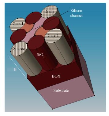
Fig. 1.
Device structure of simulated JL DG VeSFET
SEMICONDUCTOR DEVICES
Corresponding author: T. Chaudhary, Email: ctarun9@gmail.com
Abstract: This paper presents an in-depth analysis of junctionless double gate vertical slit FET (JLDG VeSFET) device under process variability. It has been observed that junctionless FETs (JLDG VeSFET) are significantly less sensitive to many process parameter variations due to their inherent device structure and geometric properties. Sensitivity analysis reveals that the slit width, oxide thickness, radius of the device, gate length and channel doping concentration imperceptibly affect the device performance of JLDG VeSFET in terms of variation in threshold voltage, on current, off current and subthreshold slope (Ssub) as compared to its junction based counterpart i.e. MOSFET, because various short channel effects are well controlled in this device. The maximum variation in off current for JLDG VeSFET due to variation in different devices parameters is 5.6% whereas this variation is 38.8% for the MOS junction based device. However, variation in doping concentration in the channel region displays a small deviation in the threshold voltage and on current characteristics of the MOSFET device as compared to JL DG VeSFET.
Keywords: JLDG VeSFET, process variation, sensitivity, scaling, short channel effects, oxide thickness, channel thickness, threshold voltage
| [1] |
International Technology Roadmap for semiconductors. 2007 Edition[Online]. Available: http://public.itrs.net/
|
| [2] |
Ghosh B, Bal P, Partha M. A junctionless tunnel field effect transistor with low subthreshold slope. J Comput Electron, 2013, 12(03):428 doi: 10.1007/s10825-013-0450-2
|
| [3] |
Wu M L, Jin X S, Chuai R Y, et al. Simulation study on short channel double-gate junctionless field effect transistor. J Semicond, 2013, 34(3):034004 doi: 10.1088/1674-4926/34/3/034004
|
| [4] |
Bendib T, Djefall F, Meguellati M. An optimized junctionless GAA MOSFET design based on multi-objective computation for high performance ultra-low power devices. J Semiconds, 2014, 35(7):074002 doi: 10.1088/1674-4926/35/7/074002
|
| [5] |
Chaudhary T, Khanna G. Compact 2-D threshold voltage model based comparative analysis of junctionless double gate VeSFET. J Nanoeng Nanomanuf; 2016, 6(02):109 doi: 10.1166/jnan.2016.1272
|
| [6] |
Chaudhary T, Khanna G. Performance enhancement and characterization of junctionless VeSFET. Int J Emerg Technol Comput Appl Sci, 2014, 8(01):309 http://yadda.icm.edu.pl/yadda/element/bwmeta1.element.baztech-article-BPOB-0042-0012
|
| [7] |
Li Y, Hwang C H, Li T Y. Process variation effect, metalgate work function and random-dopant fluctuations in emerging CMOS technologies. IEEE Trans Electron Devices, 2010, 57(2):437 doi: 10.1109/TED.2009.2036309
|
| [8] |
Li Y, Yu S M, Hwang J R. Discrete dopant fluctuations in 20 nm/15 nm gate planar CMOS. IEEE Trans Electron Devices; 2008, 55(6):1449 doi: 10.1109/TED.2008.921991
|
| [9] |
Alexander C L, Roy G, Asenov A. Random impurity scattering induced variability in conventional nano-scaled MOSFETs:ab initio impurity scattering Monte Carlo simulation study. International Electron Devices Meeting, 2006:1 http://core.ac.uk/display/9656369
|
| [10] |
Rezapour A, Rezapour P. The effect of random dopant fluctuation on threshold voltage and drain current variation in junctionless nanotransistors. J Semicond, 2015, 36(9):093002 doi: 10.1088/1674-4926/36/9/093002
|
| [11] |
Aldegunde M, Martinez A, Barker J R. Study of discrete doping induced variability in junctionless nanowire MOSFETs using dissipative quantum transport simulations. IEEE Electron Device Lett, 2012, 33(2):194 doi: 10.1109/LED.2011.2177634
|
| [12] |
Saurabh S, Jagadesh Kumar M. Estimation and compensation of process-induced variation in nanoscale tunnel field effect transistors for improved reliability. IEEE Trans Device Mater Reliab, 2010, 10(3):390 doi: 10.1109/TDMR.2010.2054095
|
| [13] |
Zhou C, Sylvester D, Blaauw D. Process variation and temperature aware reliability management. Conference on Design and Automation Test, 2010:580 https://www.date-conference.com/date15/_create_app_xml
|
| [14] |
Intekhab Amin S, Sarin R K. Analog performance investigation of misaligned double gate junctionless transistor. J Comput Electron, 2015, 14(3):675 doi: 10.1007/s10825-015-0705-1
|
| [15] |
Manna B, Sarkhel S, Islam N, et al. Spatial composition grading of binary metal alloy gate electrode short-channel SOI/SON MOSFET application. IEEE Trans Electron Devices, 2012, 59(12):3280 doi: 10.1109/TED.2012.2220143
|
| [16] |
Lilienfield J E. Method and apparatus for controlling electric current. US Patent, US1745175, 1925
|
| [17] |
Abu-Rahma M H, Anis M. A statistical design-oriented delay variation model accounting for within die variations. IEEE Trans CAD Integr Circuits Syst, 2008, 27(11):1983 doi: 10.1109/TCAD.2008.2006096
|
| [18] |
Colinge J P, Lee C W, Ferain I, et al. Reduced electric field in junctionless transistors. Appl Phys Lett, 2010, 96(7):073510 doi: 10.1063/1.3299014
|
| [19] |
Han M H, Chen C Y, Jhan Y R, et al. Characteristics of p-type junctionless gate all around nanowire transistor and sensitivity analysis. IEEE Electron Device Lett, 2013, 34(2):157 doi: 10.1109/LED.2012.2229105
|
| [20] |
Duarte J P, Chin S J, Moon D, et al. Simple analytical drain current model for long channel double gate junctionless transistor. IEEE Electron Device Lett, 2011, 32(6):704 doi: 10.1109/LED.2011.2127441
|
| [21] |
Kuhn K J, Giles M D, Becher D, et al. Process technology variation. IEEE Trans Electron Devices, 2011, 58(8):2197 doi: 10.1109/TED.2011.2121913
|
| [22] |
Mezzomo C M, Bajolet A, Cathignol A, et al. Characterization and modeling of transistor variability in advanced CMOS technologies. IEEE Trans Electron Devices, 2011, 58(8):2235 doi: 10.1109/TED.2011.2141140
|
| [23] |
Bernstein K, Frank D J, Gattiker A E, et al. High-performance CMOS variability in the 65-n regime and beyond. IBM J Res Dev, 2006, 50(4):433 http://citeseer.ist.psu.edu/showciting?cid=6027506
|
| [24] |
Springer S K, Lee S, Lu N, et al. Modeling of variation in submicrometer CMOS ULSI technologies. IEEE Trans Electron Devices, 2006, 53(9):2168 doi: 10.1109/TED.2006.880165
|
| [25] |
Saha S. Effects of inversion layer quantization on channel profile engineering for nMOSFETs with 0.1μm channel lengths. SolidState Electron, 1998, 42(11):1985 doi: 10.1016/S0038-1101(98)00183-X
|
| [26] |
Croon J A, Sansen W, Maes H E. Matching properties of deep sub micron MOS transistors. Amsterdam: Springer-Verlag, 2005
|
| [27] |
Saha S K. Compact MOSFET modeling for process variabilityaware VLSI circuit design. IEEE Access, 2014, 2:104 doi: 10.1109/ACCESS.2014.2304568
|
| [28] |
Wong A K, Ferugson R A, Mansfield S M. The mask error factor in the optical lithography. IEEE Trans Semicond Manuf, 2000, 13(2):235 doi: 10.1109/66.843639
|
| [29] |
Brunner T A. Impact of lens aberrations on optical lithography. IBM J Res Dev, 1997, 41:57 doi: 10.1147/rd.411.0057
|
| [30] |
Davis J A, Venkatesan R, Kaloyeros A, et al. Interconnect limits on giga scale integration (GSI) in the 21st century. Proc IEEE, 2001, 89(3):305 doi: 10.1109/5.915376
|
| [31] |
Raja T, Agrawal V D, Bushnell M L, et al. Transistor sizing of logic gates to maximize input delay variability. J Low Power Electron, 2006, 2(1):121 doi: 10.1166/jolpe.2006.014
|
| [32] |
Bol D, Ambroise R, Flandre D, et al. Interests and limitations of technology scaling for subthreshold logic. IEEE Trans VLSI Syst, 2009, 17(10):1508 doi: 10.1109/TVLSI.2008.2005413
|
| [33] |
Chen C Y, Lin J T, Chiang M H. Comparative study of process variations in junctionless and conventional double-gate MOSFETs. IEEE Nanotechnology Materials and Devices Conference, Taiwan, 2013
|
| [34] |
Sentaurus Structure Editor User's Manual. Synopsys International
|
| [35] |
Sentaurus Inspect User's Manual. Synopsys International
|


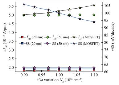
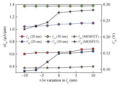
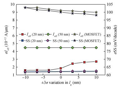


Table 1. Parameters used for process variation analysis
 |
Table 2. Summary of the variation in performance parameters values for different sources of deviation
 |
| [1] |
International Technology Roadmap for semiconductors. 2007 Edition[Online]. Available: http://public.itrs.net/
|
| [2] |
Ghosh B, Bal P, Partha M. A junctionless tunnel field effect transistor with low subthreshold slope. J Comput Electron, 2013, 12(03):428 doi: 10.1007/s10825-013-0450-2
|
| [3] |
Wu M L, Jin X S, Chuai R Y, et al. Simulation study on short channel double-gate junctionless field effect transistor. J Semicond, 2013, 34(3):034004 doi: 10.1088/1674-4926/34/3/034004
|
| [4] |
Bendib T, Djefall F, Meguellati M. An optimized junctionless GAA MOSFET design based on multi-objective computation for high performance ultra-low power devices. J Semiconds, 2014, 35(7):074002 doi: 10.1088/1674-4926/35/7/074002
|
| [5] |
Chaudhary T, Khanna G. Compact 2-D threshold voltage model based comparative analysis of junctionless double gate VeSFET. J Nanoeng Nanomanuf; 2016, 6(02):109 doi: 10.1166/jnan.2016.1272
|
| [6] |
Chaudhary T, Khanna G. Performance enhancement and characterization of junctionless VeSFET. Int J Emerg Technol Comput Appl Sci, 2014, 8(01):309 http://yadda.icm.edu.pl/yadda/element/bwmeta1.element.baztech-article-BPOB-0042-0012
|
| [7] |
Li Y, Hwang C H, Li T Y. Process variation effect, metalgate work function and random-dopant fluctuations in emerging CMOS technologies. IEEE Trans Electron Devices, 2010, 57(2):437 doi: 10.1109/TED.2009.2036309
|
| [8] |
Li Y, Yu S M, Hwang J R. Discrete dopant fluctuations in 20 nm/15 nm gate planar CMOS. IEEE Trans Electron Devices; 2008, 55(6):1449 doi: 10.1109/TED.2008.921991
|
| [9] |
Alexander C L, Roy G, Asenov A. Random impurity scattering induced variability in conventional nano-scaled MOSFETs:ab initio impurity scattering Monte Carlo simulation study. International Electron Devices Meeting, 2006:1 http://core.ac.uk/display/9656369
|
| [10] |
Rezapour A, Rezapour P. The effect of random dopant fluctuation on threshold voltage and drain current variation in junctionless nanotransistors. J Semicond, 2015, 36(9):093002 doi: 10.1088/1674-4926/36/9/093002
|
| [11] |
Aldegunde M, Martinez A, Barker J R. Study of discrete doping induced variability in junctionless nanowire MOSFETs using dissipative quantum transport simulations. IEEE Electron Device Lett, 2012, 33(2):194 doi: 10.1109/LED.2011.2177634
|
| [12] |
Saurabh S, Jagadesh Kumar M. Estimation and compensation of process-induced variation in nanoscale tunnel field effect transistors for improved reliability. IEEE Trans Device Mater Reliab, 2010, 10(3):390 doi: 10.1109/TDMR.2010.2054095
|
| [13] |
Zhou C, Sylvester D, Blaauw D. Process variation and temperature aware reliability management. Conference on Design and Automation Test, 2010:580 https://www.date-conference.com/date15/_create_app_xml
|
| [14] |
Intekhab Amin S, Sarin R K. Analog performance investigation of misaligned double gate junctionless transistor. J Comput Electron, 2015, 14(3):675 doi: 10.1007/s10825-015-0705-1
|
| [15] |
Manna B, Sarkhel S, Islam N, et al. Spatial composition grading of binary metal alloy gate electrode short-channel SOI/SON MOSFET application. IEEE Trans Electron Devices, 2012, 59(12):3280 doi: 10.1109/TED.2012.2220143
|
| [16] |
Lilienfield J E. Method and apparatus for controlling electric current. US Patent, US1745175, 1925
|
| [17] |
Abu-Rahma M H, Anis M. A statistical design-oriented delay variation model accounting for within die variations. IEEE Trans CAD Integr Circuits Syst, 2008, 27(11):1983 doi: 10.1109/TCAD.2008.2006096
|
| [18] |
Colinge J P, Lee C W, Ferain I, et al. Reduced electric field in junctionless transistors. Appl Phys Lett, 2010, 96(7):073510 doi: 10.1063/1.3299014
|
| [19] |
Han M H, Chen C Y, Jhan Y R, et al. Characteristics of p-type junctionless gate all around nanowire transistor and sensitivity analysis. IEEE Electron Device Lett, 2013, 34(2):157 doi: 10.1109/LED.2012.2229105
|
| [20] |
Duarte J P, Chin S J, Moon D, et al. Simple analytical drain current model for long channel double gate junctionless transistor. IEEE Electron Device Lett, 2011, 32(6):704 doi: 10.1109/LED.2011.2127441
|
| [21] |
Kuhn K J, Giles M D, Becher D, et al. Process technology variation. IEEE Trans Electron Devices, 2011, 58(8):2197 doi: 10.1109/TED.2011.2121913
|
| [22] |
Mezzomo C M, Bajolet A, Cathignol A, et al. Characterization and modeling of transistor variability in advanced CMOS technologies. IEEE Trans Electron Devices, 2011, 58(8):2235 doi: 10.1109/TED.2011.2141140
|
| [23] |
Bernstein K, Frank D J, Gattiker A E, et al. High-performance CMOS variability in the 65-n regime and beyond. IBM J Res Dev, 2006, 50(4):433 http://citeseer.ist.psu.edu/showciting?cid=6027506
|
| [24] |
Springer S K, Lee S, Lu N, et al. Modeling of variation in submicrometer CMOS ULSI technologies. IEEE Trans Electron Devices, 2006, 53(9):2168 doi: 10.1109/TED.2006.880165
|
| [25] |
Saha S. Effects of inversion layer quantization on channel profile engineering for nMOSFETs with 0.1μm channel lengths. SolidState Electron, 1998, 42(11):1985 doi: 10.1016/S0038-1101(98)00183-X
|
| [26] |
Croon J A, Sansen W, Maes H E. Matching properties of deep sub micron MOS transistors. Amsterdam: Springer-Verlag, 2005
|
| [27] |
Saha S K. Compact MOSFET modeling for process variabilityaware VLSI circuit design. IEEE Access, 2014, 2:104 doi: 10.1109/ACCESS.2014.2304568
|
| [28] |
Wong A K, Ferugson R A, Mansfield S M. The mask error factor in the optical lithography. IEEE Trans Semicond Manuf, 2000, 13(2):235 doi: 10.1109/66.843639
|
| [29] |
Brunner T A. Impact of lens aberrations on optical lithography. IBM J Res Dev, 1997, 41:57 doi: 10.1147/rd.411.0057
|
| [30] |
Davis J A, Venkatesan R, Kaloyeros A, et al. Interconnect limits on giga scale integration (GSI) in the 21st century. Proc IEEE, 2001, 89(3):305 doi: 10.1109/5.915376
|
| [31] |
Raja T, Agrawal V D, Bushnell M L, et al. Transistor sizing of logic gates to maximize input delay variability. J Low Power Electron, 2006, 2(1):121 doi: 10.1166/jolpe.2006.014
|
| [32] |
Bol D, Ambroise R, Flandre D, et al. Interests and limitations of technology scaling for subthreshold logic. IEEE Trans VLSI Syst, 2009, 17(10):1508 doi: 10.1109/TVLSI.2008.2005413
|
| [33] |
Chen C Y, Lin J T, Chiang M H. Comparative study of process variations in junctionless and conventional double-gate MOSFETs. IEEE Nanotechnology Materials and Devices Conference, Taiwan, 2013
|
| [34] |
Sentaurus Structure Editor User's Manual. Synopsys International
|
| [35] |
Sentaurus Inspect User's Manual. Synopsys International
|


Article views: 4233 Times PDF downloads: 31 Times Cited by: 0 Times
Received: 02 February 2017 Revised: 19 April 2017 Online: Published: 01 October 2017
| Citation: |
T. Chaudhary, G. Khanna. Analysis and impact of process variability on performance of junctionless double gate VeSFET[J]. Journal of Semiconductors, 2017, 38(10): 104003. doi: 10.1088/1674-4926/38/10/104003
****
T. Chaudhary, G. Khanna. Analysis and impact of process variability on performance of junctionless double gate VeSFET[J]. J. Semicond., 2017, 38(10): 104003. doi: 10.1088/1674-4926/38/10/104003.

|
| [1] |
International Technology Roadmap for semiconductors. 2007 Edition[Online]. Available: http://public.itrs.net/
|
| [2] |
Ghosh B, Bal P, Partha M. A junctionless tunnel field effect transistor with low subthreshold slope. J Comput Electron, 2013, 12(03):428 doi: 10.1007/s10825-013-0450-2
|
| [3] |
Wu M L, Jin X S, Chuai R Y, et al. Simulation study on short channel double-gate junctionless field effect transistor. J Semicond, 2013, 34(3):034004 doi: 10.1088/1674-4926/34/3/034004
|
| [4] |
Bendib T, Djefall F, Meguellati M. An optimized junctionless GAA MOSFET design based on multi-objective computation for high performance ultra-low power devices. J Semiconds, 2014, 35(7):074002 doi: 10.1088/1674-4926/35/7/074002
|
| [5] |
Chaudhary T, Khanna G. Compact 2-D threshold voltage model based comparative analysis of junctionless double gate VeSFET. J Nanoeng Nanomanuf; 2016, 6(02):109 doi: 10.1166/jnan.2016.1272
|
| [6] |
Chaudhary T, Khanna G. Performance enhancement and characterization of junctionless VeSFET. Int J Emerg Technol Comput Appl Sci, 2014, 8(01):309 http://yadda.icm.edu.pl/yadda/element/bwmeta1.element.baztech-article-BPOB-0042-0012
|
| [7] |
Li Y, Hwang C H, Li T Y. Process variation effect, metalgate work function and random-dopant fluctuations in emerging CMOS technologies. IEEE Trans Electron Devices, 2010, 57(2):437 doi: 10.1109/TED.2009.2036309
|
| [8] |
Li Y, Yu S M, Hwang J R. Discrete dopant fluctuations in 20 nm/15 nm gate planar CMOS. IEEE Trans Electron Devices; 2008, 55(6):1449 doi: 10.1109/TED.2008.921991
|
| [9] |
Alexander C L, Roy G, Asenov A. Random impurity scattering induced variability in conventional nano-scaled MOSFETs:ab initio impurity scattering Monte Carlo simulation study. International Electron Devices Meeting, 2006:1 http://core.ac.uk/display/9656369
|
| [10] |
Rezapour A, Rezapour P. The effect of random dopant fluctuation on threshold voltage and drain current variation in junctionless nanotransistors. J Semicond, 2015, 36(9):093002 doi: 10.1088/1674-4926/36/9/093002
|
| [11] |
Aldegunde M, Martinez A, Barker J R. Study of discrete doping induced variability in junctionless nanowire MOSFETs using dissipative quantum transport simulations. IEEE Electron Device Lett, 2012, 33(2):194 doi: 10.1109/LED.2011.2177634
|
| [12] |
Saurabh S, Jagadesh Kumar M. Estimation and compensation of process-induced variation in nanoscale tunnel field effect transistors for improved reliability. IEEE Trans Device Mater Reliab, 2010, 10(3):390 doi: 10.1109/TDMR.2010.2054095
|
| [13] |
Zhou C, Sylvester D, Blaauw D. Process variation and temperature aware reliability management. Conference on Design and Automation Test, 2010:580 https://www.date-conference.com/date15/_create_app_xml
|
| [14] |
Intekhab Amin S, Sarin R K. Analog performance investigation of misaligned double gate junctionless transistor. J Comput Electron, 2015, 14(3):675 doi: 10.1007/s10825-015-0705-1
|
| [15] |
Manna B, Sarkhel S, Islam N, et al. Spatial composition grading of binary metal alloy gate electrode short-channel SOI/SON MOSFET application. IEEE Trans Electron Devices, 2012, 59(12):3280 doi: 10.1109/TED.2012.2220143
|
| [16] |
Lilienfield J E. Method and apparatus for controlling electric current. US Patent, US1745175, 1925
|
| [17] |
Abu-Rahma M H, Anis M. A statistical design-oriented delay variation model accounting for within die variations. IEEE Trans CAD Integr Circuits Syst, 2008, 27(11):1983 doi: 10.1109/TCAD.2008.2006096
|
| [18] |
Colinge J P, Lee C W, Ferain I, et al. Reduced electric field in junctionless transistors. Appl Phys Lett, 2010, 96(7):073510 doi: 10.1063/1.3299014
|
| [19] |
Han M H, Chen C Y, Jhan Y R, et al. Characteristics of p-type junctionless gate all around nanowire transistor and sensitivity analysis. IEEE Electron Device Lett, 2013, 34(2):157 doi: 10.1109/LED.2012.2229105
|
| [20] |
Duarte J P, Chin S J, Moon D, et al. Simple analytical drain current model for long channel double gate junctionless transistor. IEEE Electron Device Lett, 2011, 32(6):704 doi: 10.1109/LED.2011.2127441
|
| [21] |
Kuhn K J, Giles M D, Becher D, et al. Process technology variation. IEEE Trans Electron Devices, 2011, 58(8):2197 doi: 10.1109/TED.2011.2121913
|
| [22] |
Mezzomo C M, Bajolet A, Cathignol A, et al. Characterization and modeling of transistor variability in advanced CMOS technologies. IEEE Trans Electron Devices, 2011, 58(8):2235 doi: 10.1109/TED.2011.2141140
|
| [23] |
Bernstein K, Frank D J, Gattiker A E, et al. High-performance CMOS variability in the 65-n regime and beyond. IBM J Res Dev, 2006, 50(4):433 http://citeseer.ist.psu.edu/showciting?cid=6027506
|
| [24] |
Springer S K, Lee S, Lu N, et al. Modeling of variation in submicrometer CMOS ULSI technologies. IEEE Trans Electron Devices, 2006, 53(9):2168 doi: 10.1109/TED.2006.880165
|
| [25] |
Saha S. Effects of inversion layer quantization on channel profile engineering for nMOSFETs with 0.1μm channel lengths. SolidState Electron, 1998, 42(11):1985 doi: 10.1016/S0038-1101(98)00183-X
|
| [26] |
Croon J A, Sansen W, Maes H E. Matching properties of deep sub micron MOS transistors. Amsterdam: Springer-Verlag, 2005
|
| [27] |
Saha S K. Compact MOSFET modeling for process variabilityaware VLSI circuit design. IEEE Access, 2014, 2:104 doi: 10.1109/ACCESS.2014.2304568
|
| [28] |
Wong A K, Ferugson R A, Mansfield S M. The mask error factor in the optical lithography. IEEE Trans Semicond Manuf, 2000, 13(2):235 doi: 10.1109/66.843639
|
| [29] |
Brunner T A. Impact of lens aberrations on optical lithography. IBM J Res Dev, 1997, 41:57 doi: 10.1147/rd.411.0057
|
| [30] |
Davis J A, Venkatesan R, Kaloyeros A, et al. Interconnect limits on giga scale integration (GSI) in the 21st century. Proc IEEE, 2001, 89(3):305 doi: 10.1109/5.915376
|
| [31] |
Raja T, Agrawal V D, Bushnell M L, et al. Transistor sizing of logic gates to maximize input delay variability. J Low Power Electron, 2006, 2(1):121 doi: 10.1166/jolpe.2006.014
|
| [32] |
Bol D, Ambroise R, Flandre D, et al. Interests and limitations of technology scaling for subthreshold logic. IEEE Trans VLSI Syst, 2009, 17(10):1508 doi: 10.1109/TVLSI.2008.2005413
|
| [33] |
Chen C Y, Lin J T, Chiang M H. Comparative study of process variations in junctionless and conventional double-gate MOSFETs. IEEE Nanotechnology Materials and Devices Conference, Taiwan, 2013
|
| [34] |
Sentaurus Structure Editor User's Manual. Synopsys International
|
| [35] |
Sentaurus Inspect User's Manual. Synopsys International
|

 WeChat ID
Journal of Semiconductors © 2017 All Rights Reserved 京ICP备05085259号-2

 DownLoad:

