


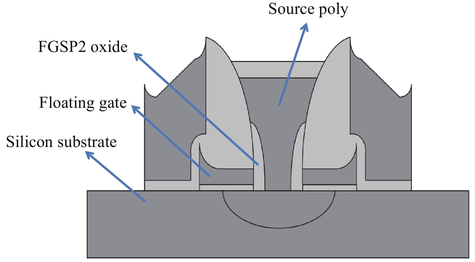
Fig. 1.
(Color online) Split-gate flash cell structure.
SEMICONDUCTOR TECHNOLOGY
Dailong Wei, Zigui Cao and Zhilin Tang
Corresponding author: † Dailong.Wei@hhgrace.com
Abstract: Data retention is one of the most important reliability characteristics of split-gate flash. Therefore, many efforts were made to improve data retention of split-gate flash. By experiments, it was found that higher chlorine concentration produced in FGSP2 oxide deposition can induce worse data retention. Thus, reducing chlorine concentration is an effective approach to improve data retention for split-gate flash product. Additional RTO annealing between FGSP2 oxide deposition and FGSP2 etching could reduce chlorine concentration, and improve FGSP2 oxide film quality, and then get better data retention.
Keywords: split-gate flash, data retention, RTO anneal
| [1] |
Bez R, Camerlenghi E, Modelli A, et al. Introduction to flash memory. Proc IEEE, 2003, 91(4): 489 doi: 10.1109/JPROC.2003.811702
|
| [2] |
Pavan P, Bez R, Olivo P, et al. Flash memory cells-an overview. Proc IEEE, 1997, 85(8): 1248 doi: 10.1109/5.622505
|
| [3] |
Aritome S. Advanced flash memory technology and trends for file storage application. Electron Devices Meeting, 2000
|
| [4] |
Chang K T, Chen W M, Swift C, et al. A new SONOS memory using source-side injection for programming. IEEE Electron Device Lett, 1998, 19(7): 253 doi: 10.1109/55.701434
|
| [5] |
Van Houdt J F, Groeseneken G, Maes H E. An analytical model for the optimization of source-side injection flash EEPROM devices. IEEE Trans Electron Devices, 1995, 42(7): 1314 doi: 10.1109/16.391214
|
| [6] |
Wu A T, Chan T Y, Ko P K, et al. A novel high-speed, 5-volt programming EPROM structure with source-side injection. Electron Devices Meeting, 1986
|
| [7] |
Ma Y, Pang C S, Pathak J, et al. A novel high density contactless flash memory array using split-gate source-side injection cell for 5 V-only application. 1994 Symposium on VLSI Technol, 1994
|
| [8] |
Lee Y K, Min H, Jeon C, et al. Highly scalable 2nd-generation 45-nm split-gate embedded flash with 10-ns access time and 1M-cycling endurance. Memory Workshop (IMW), 2016
|
| [9] |
Kono T, Ito T, Tsuruda T, et al. 40-nm embedded split-gate MONOS (SG-MONOS) flash macros for automotive with 160-MHz random access for code and endurance over 10 M cycles for data at the junction temperature of 170 °C. IEEE J Solid-State Circuits, 2014, 49(1): 154 doi: 10.1109/JSSC.2013.2280303
|
| [10] |
Nhan Do N. Scaling of split-gate flash memory and its adoption in modern embedded non-volatile applications. International Conference on IC Design and Technology, 2016
|
| [11] |
Cho C Y, Chen M J, Chen C F, et al. A novel self-aligned highly reliable sidewall split-gate flash memory. IEEE Trans Electron Devices, 2006, 53(3): 465 doi: 10.1109/TED.2005.863764
|
| [12] |
Saha S K. Design considerations for sub-90-nm split-gate flash memory cells. IEEE Trans Electron Devices, 2007, 54(11): 3046
|
| [13] |
Weinberg Z A, Young D R, Calise J A, et al. Reduction of electron and hole trapping in SiO2 by rapid thermal annealing. Appl Phys Lett, 1984, 45: 1204 doi: 10.1063/1.95098
|
| [14] |
van der Meulen Y J, Osburn C M, Ziegler J F. Properties of SiO2 grown in the presence of HCI or CI2. J Electrochem Soc, 1975, 122(2): 284 doi: 10.1149/1.2134196
|
| [15] |
Nishioka Y, Da Silva E F, Wang Y, et al. Dramatic improvement of hot-electron-induced interface degradation in MOS structures containing F or Cl in SiO2. IEEE Electron Device Lett, 1988, 9(1): 38 doi: 10.1109/55.20406
|
| [16] |
Nasyrov K A, Shaimeev S S, Gritsenko V A. Trap-assisted tunneling hole injection in SiO2: experiment and theory. J Exp Theor Phys, 2009, 109(5): 786 doi: 10.1134/S1063776109110089
|
| [17] |
Chou A I, Lai K F, Kumar K, et al. Modeling of stress-induced leakage current in ultrathin oxides with the trap-assisted tunneling mechanism. Appl Phys Lett, 1997, 70: 3407 doi: 10.1063/1.119186
|
| [18] |
Jiménez-Molinos F, Palma A, Gámiz F, et al. Physical model for trap-assisted inelastic tunneling in metal–oxide–semiconductor structures. J Appl Phys, 2001, 90: 3396 doi: 10.1063/1.1398603
|
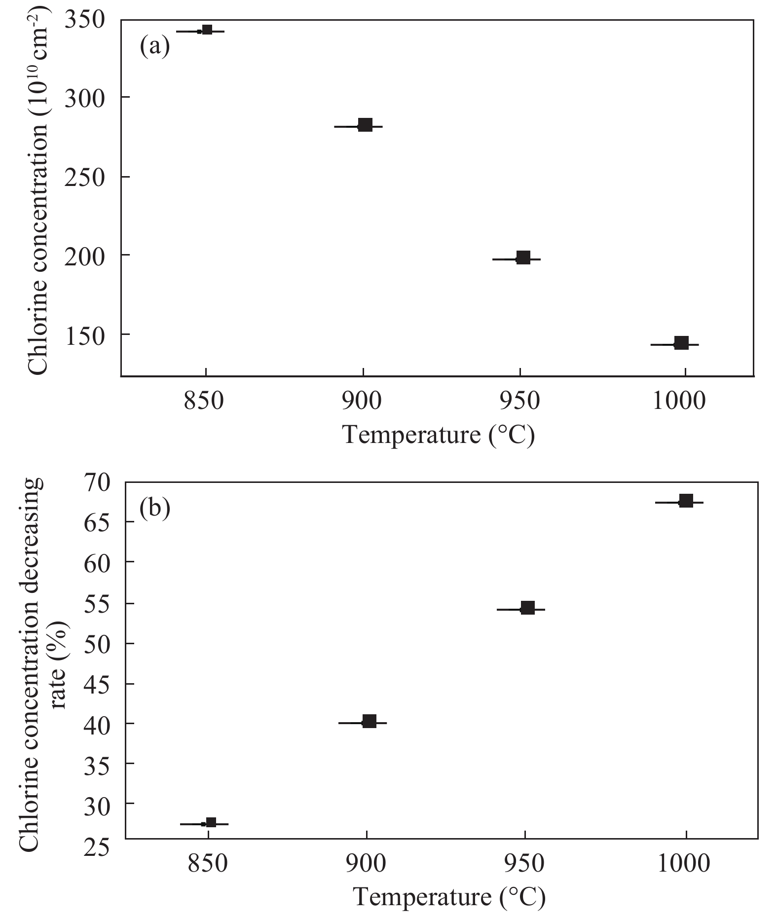
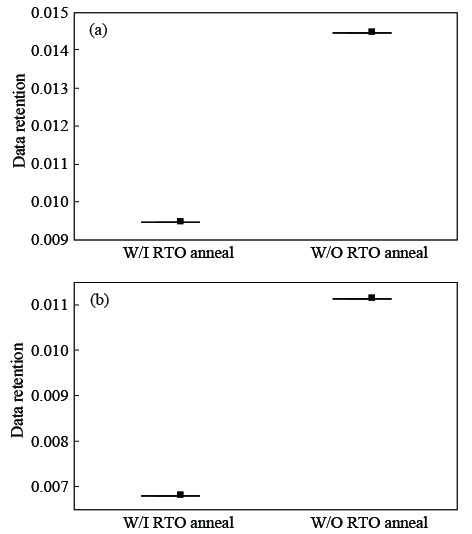
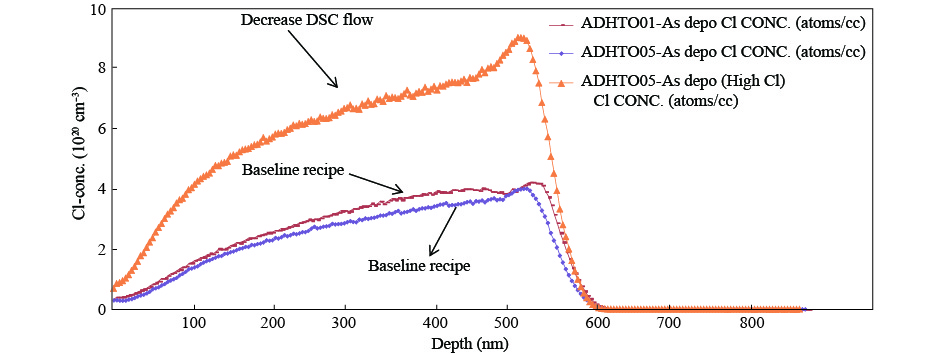
Table 1. Different annealing temperatures with additional RTO annealing process.
| Samples-No. | Annealingtemperature (°C) | O2 (slm) | N2 (slm) | Annealingtime (s) |
| 1 | 850 | 1 | 5 | 90 |
| 2 | 900 | 1 | 5 | 90 |
| 3 | 950 | 1 | 5 | 90 |
| 4 | 1000 | 1 | 5 | 90 |
 DownLoad: CSV
Table 2. Different products W/I and W/O RTO annealing process.
| Sample | RTO annealing process | Annealing temperature (°C) | O2 (slm) | N2 (slm) | Annealingtime (s) |
| Product1 | Add | 1000 | 1 | 5 | 90 |
| Product1 | NA | ||||
| Product2 | Add | 1000 | 1 | 5 | 90 |
| Product2 | NA |
DownLoad: CSV
Table 3. FGSP2 oxide deposition with different tools or different source amounts.
| Samples-No. | FGSP2 DEP tool | DCS | N2O |
| A | ADHTO01 | Baseline | Baseline |
| B | ADHTO05 | Baseline | Baseline |
| C | ADHTO05 | Baseline-10% | Baseline |
DownLoad: CSV
| [1] |
Bez R, Camerlenghi E, Modelli A, et al. Introduction to flash memory. Proc IEEE, 2003, 91(4): 489 doi: 10.1109/JPROC.2003.811702
|
| [2] |
Pavan P, Bez R, Olivo P, et al. Flash memory cells-an overview. Proc IEEE, 1997, 85(8): 1248 doi: 10.1109/5.622505
|
| [3] |
Aritome S. Advanced flash memory technology and trends for file storage application. Electron Devices Meeting, 2000
|
| [4] |
Chang K T, Chen W M, Swift C, et al. A new SONOS memory using source-side injection for programming. IEEE Electron Device Lett, 1998, 19(7): 253 doi: 10.1109/55.701434
|
| [5] |
Van Houdt J F, Groeseneken G, Maes H E. An analytical model for the optimization of source-side injection flash EEPROM devices. IEEE Trans Electron Devices, 1995, 42(7): 1314 doi: 10.1109/16.391214
|
| [6] |
Wu A T, Chan T Y, Ko P K, et al. A novel high-speed, 5-volt programming EPROM structure with source-side injection. Electron Devices Meeting, 1986
|
| [7] |
Ma Y, Pang C S, Pathak J, et al. A novel high density contactless flash memory array using split-gate source-side injection cell for 5 V-only application. 1994 Symposium on VLSI Technol, 1994
|
| [8] |
Lee Y K, Min H, Jeon C, et al. Highly scalable 2nd-generation 45-nm split-gate embedded flash with 10-ns access time and 1M-cycling endurance. Memory Workshop (IMW), 2016
|
| [9] |
Kono T, Ito T, Tsuruda T, et al. 40-nm embedded split-gate MONOS (SG-MONOS) flash macros for automotive with 160-MHz random access for code and endurance over 10 M cycles for data at the junction temperature of 170 °C. IEEE J Solid-State Circuits, 2014, 49(1): 154 doi: 10.1109/JSSC.2013.2280303
|
| [10] |
Nhan Do N. Scaling of split-gate flash memory and its adoption in modern embedded non-volatile applications. International Conference on IC Design and Technology, 2016
|
| [11] |
Cho C Y, Chen M J, Chen C F, et al. A novel self-aligned highly reliable sidewall split-gate flash memory. IEEE Trans Electron Devices, 2006, 53(3): 465 doi: 10.1109/TED.2005.863764
|
| [12] |
Saha S K. Design considerations for sub-90-nm split-gate flash memory cells. IEEE Trans Electron Devices, 2007, 54(11): 3046
|
| [13] |
Weinberg Z A, Young D R, Calise J A, et al. Reduction of electron and hole trapping in SiO2 by rapid thermal annealing. Appl Phys Lett, 1984, 45: 1204 doi: 10.1063/1.95098
|
| [14] |
van der Meulen Y J, Osburn C M, Ziegler J F. Properties of SiO2 grown in the presence of HCI or CI2. J Electrochem Soc, 1975, 122(2): 284 doi: 10.1149/1.2134196
|
| [15] |
Nishioka Y, Da Silva E F, Wang Y, et al. Dramatic improvement of hot-electron-induced interface degradation in MOS structures containing F or Cl in SiO2. IEEE Electron Device Lett, 1988, 9(1): 38 doi: 10.1109/55.20406
|
| [16] |
Nasyrov K A, Shaimeev S S, Gritsenko V A. Trap-assisted tunneling hole injection in SiO2: experiment and theory. J Exp Theor Phys, 2009, 109(5): 786 doi: 10.1134/S1063776109110089
|
| [17] |
Chou A I, Lai K F, Kumar K, et al. Modeling of stress-induced leakage current in ultrathin oxides with the trap-assisted tunneling mechanism. Appl Phys Lett, 1997, 70: 3407 doi: 10.1063/1.119186
|
| [18] |
Jiménez-Molinos F, Palma A, Gámiz F, et al. Physical model for trap-assisted inelastic tunneling in metal–oxide–semiconductor structures. J Appl Phys, 2001, 90: 3396 doi: 10.1063/1.1398603
|


Article views: 4374 Times PDF downloads: 59 Times Cited by: 0 Times
Received: 01 November 2016 Revised: 20 April 2017 Online: Accepted Manuscript: 13 November 2017Published: 01 October 2017
| Citation: |
Dailong Wei, Zigui Cao, Zhilin Tang. An effective approach to improve split-gate flash product data retention[J]. Journal of Semiconductors, 2017, 38(10): 106001. doi: 10.1088/1674-4926/38/10/106001
****
D L Wei, Z G Cao, Z L Tang. An effective approach to improve split-gate flash product data retention[J]. J. Semicond., 2017, 38(10): 106001. doi: 10.1088/1674-4926/38/10/106001.

|
| [1] |
Bez R, Camerlenghi E, Modelli A, et al. Introduction to flash memory. Proc IEEE, 2003, 91(4): 489 doi: 10.1109/JPROC.2003.811702
|
| [2] |
Pavan P, Bez R, Olivo P, et al. Flash memory cells-an overview. Proc IEEE, 1997, 85(8): 1248 doi: 10.1109/5.622505
|
| [3] |
Aritome S. Advanced flash memory technology and trends for file storage application. Electron Devices Meeting, 2000
|
| [4] |
Chang K T, Chen W M, Swift C, et al. A new SONOS memory using source-side injection for programming. IEEE Electron Device Lett, 1998, 19(7): 253 doi: 10.1109/55.701434
|
| [5] |
Van Houdt J F, Groeseneken G, Maes H E. An analytical model for the optimization of source-side injection flash EEPROM devices. IEEE Trans Electron Devices, 1995, 42(7): 1314 doi: 10.1109/16.391214
|
| [6] |
Wu A T, Chan T Y, Ko P K, et al. A novel high-speed, 5-volt programming EPROM structure with source-side injection. Electron Devices Meeting, 1986
|
| [7] |
Ma Y, Pang C S, Pathak J, et al. A novel high density contactless flash memory array using split-gate source-side injection cell for 5 V-only application. 1994 Symposium on VLSI Technol, 1994
|
| [8] |
Lee Y K, Min H, Jeon C, et al. Highly scalable 2nd-generation 45-nm split-gate embedded flash with 10-ns access time and 1M-cycling endurance. Memory Workshop (IMW), 2016
|
| [9] |
Kono T, Ito T, Tsuruda T, et al. 40-nm embedded split-gate MONOS (SG-MONOS) flash macros for automotive with 160-MHz random access for code and endurance over 10 M cycles for data at the junction temperature of 170 °C. IEEE J Solid-State Circuits, 2014, 49(1): 154 doi: 10.1109/JSSC.2013.2280303
|
| [10] |
Nhan Do N. Scaling of split-gate flash memory and its adoption in modern embedded non-volatile applications. International Conference on IC Design and Technology, 2016
|
| [11] |
Cho C Y, Chen M J, Chen C F, et al. A novel self-aligned highly reliable sidewall split-gate flash memory. IEEE Trans Electron Devices, 2006, 53(3): 465 doi: 10.1109/TED.2005.863764
|
| [12] |
Saha S K. Design considerations for sub-90-nm split-gate flash memory cells. IEEE Trans Electron Devices, 2007, 54(11): 3046
|
| [13] |
Weinberg Z A, Young D R, Calise J A, et al. Reduction of electron and hole trapping in SiO2 by rapid thermal annealing. Appl Phys Lett, 1984, 45: 1204 doi: 10.1063/1.95098
|
| [14] |
van der Meulen Y J, Osburn C M, Ziegler J F. Properties of SiO2 grown in the presence of HCI or CI2. J Electrochem Soc, 1975, 122(2): 284 doi: 10.1149/1.2134196
|
| [15] |
Nishioka Y, Da Silva E F, Wang Y, et al. Dramatic improvement of hot-electron-induced interface degradation in MOS structures containing F or Cl in SiO2. IEEE Electron Device Lett, 1988, 9(1): 38 doi: 10.1109/55.20406
|
| [16] |
Nasyrov K A, Shaimeev S S, Gritsenko V A. Trap-assisted tunneling hole injection in SiO2: experiment and theory. J Exp Theor Phys, 2009, 109(5): 786 doi: 10.1134/S1063776109110089
|
| [17] |
Chou A I, Lai K F, Kumar K, et al. Modeling of stress-induced leakage current in ultrathin oxides with the trap-assisted tunneling mechanism. Appl Phys Lett, 1997, 70: 3407 doi: 10.1063/1.119186
|
| [18] |
Jiménez-Molinos F, Palma A, Gámiz F, et al. Physical model for trap-assisted inelastic tunneling in metal–oxide–semiconductor structures. J Appl Phys, 2001, 90: 3396 doi: 10.1063/1.1398603
|

 WeChat ID
Journal of Semiconductors © 2017 All Rights Reserved 京ICP备05085259号-2


