| Citation: |
Manoj Kumar, Yogesh Pratap, Subhasis Haldar, Mridula Gupta, R. S. Gupta. Cylindrical gate all around Schottky barrier MOSFET with insulated shallow extensions at source/drain for removal of ambipolarity: a novel approach[J]. Journal of Semiconductors, 2017, 38(12): 124002. doi: 10.1088/1674-4926/38/12/124002
****
M Kumar, Y Pratap, S Haldar, M Gupta, R. S. Gupta. Cylindrical gate all around Schottky barrier MOSFET with insulated shallow extensions at source/drain for removal of ambipolarity: a novel approach[J]. J. Semicond., 2017, 38(12): 124002. doi: 10.1088/1674-4926/38/12/124002.
|
Cylindrical gate all around Schottky barrier MOSFET with insulated shallow extensions at source/drain for removal of ambipolarity: a novel approach
DOI: 10.1088/1674-4926/38/12/124002
More Information
-
Abstract
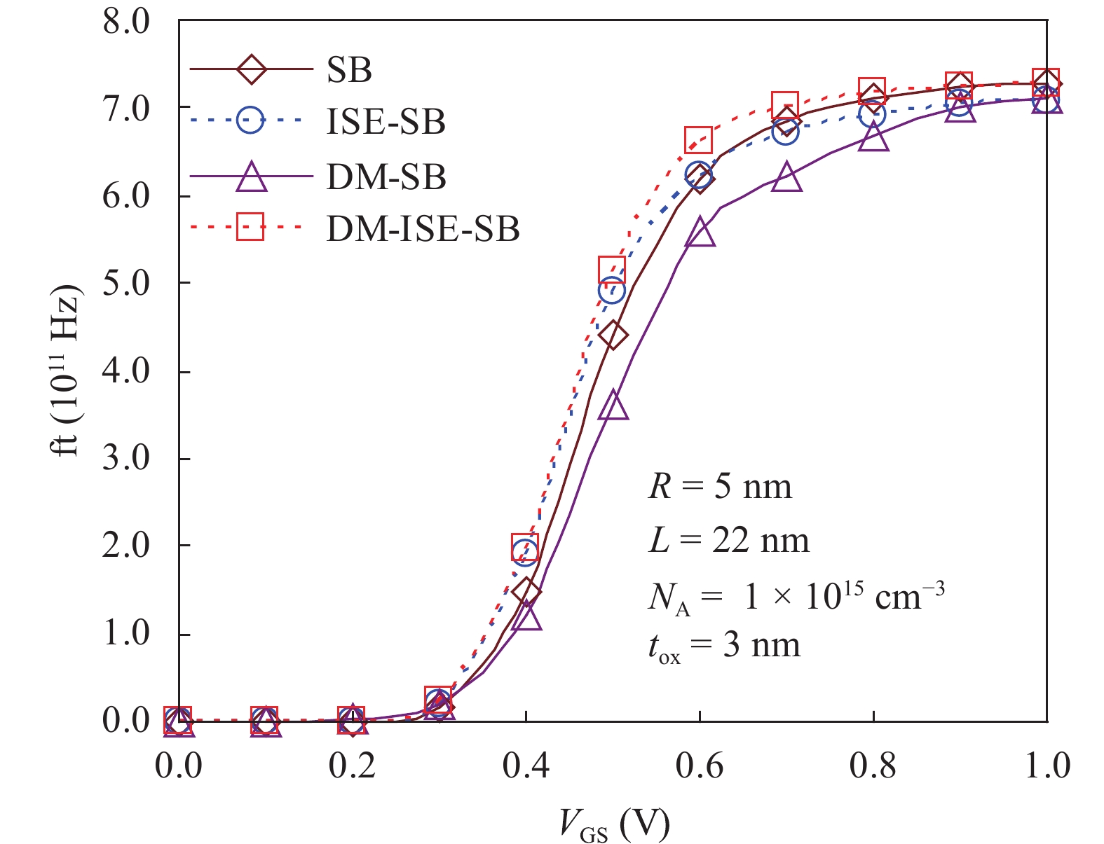
In this paper TCAD-based simulation of a novel insulated shallow extension (ISE) cylindrical gate all around (CGAA) Schottky barrier (SB) MOSFET has been reported, to eliminate the suicidal ambipolar behavior (bias-dependent OFF state leakage current) of conventional SB-CGAA MOSFET by blocking the metal-induced gap states as well as unwanted charge sharing between source/channel and drain/channel regions. This novel structure offers low barrier height at the source and offers high ON-state current. The ION/IOFF of ISE-CGAA-SB-MOSFET increases by 1177 times and offers steeper subthreshold slope (~60 mV/decade). However a little reduction in peak cut off frequency is observed and to further improve the cut-off frequency dual metal gate architecture has been employed and a comparative assessment of single metal gate, dual metal gate, single metal gate with ISE, and dual metal gate with ISE has been presented. The improved performance of Schottky barrier CGAA MOSFET by the incorporation of ISE makes it an attractive candidate for CMOS digital circuit design. The numerical simulation is performed using the ATLAS-3D device simulator. -
References
[1] Ferain I, Coling C A, Colinge J P. Multigate transistor as the future of classical metal–oxide–semiconductor field-effect transistors. Nature, 2011, 479: 310 doi: 10.1038/nature10676[2] Zhang Y, Li Z, Wang C, et al. Compact analytical threshold voltage model of strained gate-all around MOSFET fabricated on Si1−xGex virtual substrate. IEICE Trans Electron, 2016, E99-C: 302 doi: 10.1587/transele.E99.C.302[3] Cheng Q, Hong C, Kuo J B, et al. A Surface-Field-Based Model for Nanowire MOSFETs With Spatial Variations of Doping Profiles. IEEE Trans Electron Devices, 2014, 61: 4040 doi: 10.1109/TED.2014.2364781[4] Cheng H, Uno S, Nakazato K. Analytical compact model of ballistic and quasi-ballistic transport for cylindrical gat-all-around MOSFET including drain-induced barrier lowering effect. J Comput Electron, 2014, 14: 321[5] Larson J M, Snyder J P. Overview and status of metal S/D Schottky-barrier MOSFET technology. IEEE Trans Electron Devices, 2006, 53: 1048 doi: 10.1109/TED.2006.871842[6] Thompson S, Parthasarathy S. Mooer's Law: the future of Si microelectronics. Mater Today, 2006, 9: 20[7] Kedzierski J, Xuan P, Andeson E H, et al. Complementary silicide source/drain thin-body MOSFT for the 20 nm gate length regime. IEEE International Electron Devices Meeting (IEDM), 2000: 57[8] Martin-Martinez M J, Couso C, Pascual E, et al. Monte Carlo study of dopant-segregated Schottky Barrier DoIMOSFETs: enhancement of the RF performance. IEEE Trans Electron Devices, 2014, 61: 3955 doi: 10.1109/TED.2014.2360468[9] Zhu G, Zhou X, Lee T S, et al. A compact model for undoped silicon-nanowire MOSFETs with schottky-barrier source/drain. IEEE Trans Electron Devices, 2009, 56: 1100 doi: 10.1109/TED.2009.2015161[10] Choi S J, Cho Y K. Source and drain junction engineering for enhanced non-volatile memory performance. Igor Stievano ed. Flash Memories, InTech, 2011[11] Kumar M, Haldar S, Gupta M, et al. Physics based analytical model for surface potential and subthreshold current of cylindrical Schottky barrier gate all around MOSFET with high-k gate stack. Superlattices Microstruct, 20116, 90: 215 doi: 10.1016/j.spmi.2015.12.029[12] Östling M, Gudmundsson V, Hellström P E, et al. Towards Schottky-barrier source/drain MOSFETs. 9th International Conference on Solid-State and Integrated-Circuit Technology (ICSICT), 2008: 146[13] Saad I, Bolong N, Divya P, et al. Performance design and simulation analysis of vertical double gate MOSFET (VDGM). UKSim 13th International Conference on Modelling and Simulation, 2011[14] Trivedi N, Kumar M, Haldar S, et al. Aanalytical modelling of junctionless accumulation mode cylindrical surrounding gate MOSFET (JAM CSG). Int J Numerical Model,[15] Jurczak M, Skotnicki T, Gwoziecki R, et al. Dielectric pockets-a new concept of the junctions for deca-nanometric CMOS devices. IEEE Trans Electron Devices, 2001, 48: 952[16] Kok O P, Ibrahim K. Simulation of two-dimensional 50 nm vertical metal oxide semiconductor field effect transistor incorporating a dielectric pocket. Jpn J Appl Phys, 2009, 48: 111201 doi: 10.1143/JJAP.48.111201[17] Ghoneim H, Konch J, Riel H, et al. Interface engineering for the suppression of ambipolar behavior in Schottky-barrier MOSFET. 10th International Conference on Ultimate Integration of Silicon, 2009: 69[18] Ghoneim H, Knoch J, Riel H, et al. Suppression of ambipolar behaviour in metallic source/drain metal oxide-semiconductor field-effect transistors. Appl Phys Lett, 2009, 95: 213504 doi: 10.1063/1.3266526[19] Kumari V, Saxena M, Gupta R S, et al. Two dimensional analytical drain current model for double gate MOSFET incorporating dielectric pocket. IEEE Trans Electron Devices, 2012, 59: 2567 doi: 10.1109/TED.2012.2206030[20] Singh B, Gola D, Goel E, et al. Dielectric pocket double gate junctionless FET: a new MOS structure with improved subthreshold characteristics for low power VLSI applications. J Comput Electron, 2016, 15: 502 doi: 10.1007/s10825-016-0808-3[21] Wang H, Wang Z. Dielectric plug in MOSFETs to suppress short-channel effects. US Patent 7154146 B2, 2006[22] Kumari V, Saxena M, Gupta R S, et al. Temperature dependent drain current model for Gate Stack Insulated Shallow Extension Silicon On Nothing (ISESON) MOSFET for wide operating temperature range. Microelectron Reliab, 2012, 52: 974 doi: 10.1016/j.microrel.2011.12.021[23] Lin R, Lu Q, Ranade P, et al. An adjustable workfunction technology using Mo gate for CMOS devices. IEEE Electron Devices Lett, 2002, 23: 49 doi: 10.1109/55.974809[24] Lu Q, Yeo Y C, Ranade P H, et al. Dual-metal gate technology for deep-submicron CMOS transistors. Symp VLSI Technol, 2000: 72[25] Tsui B Y, Huang S F. Wide range workfunction modulation of binary alloy for MOSFET application. IEEE Electron Device Lett, 2003, 24: 153 doi: 10.1109/LED.2003.809528[26] Schwarz M, Kloes A. Analysis and performance study of III–V Schottky Barrier Double-Gate MOSFET using a 2-D analytical Model. IEEE Trans Electron Devices, 2016, 63: 2757 doi: 10.1109/TED.2016.2569488[27] Trivedi V P, Fossum J G. Quantum-mechanical effects on the threshold voltage of undoped double-gate MOSFETs. IEEE Electron Device Lett, 2005, 26: 579 doi: 10.1109/LED.2005.852741[28] Omura Y, Horiguchi S, Tabe M, et al. Quantum-mechanical effects on the threshold voltage of ultrathin-SOI nMOSFETs. IEEE Electron Device Lett, 1993, 14: 569 doi: 10.1109/55.260792[29] ATLAS User's Manual. 3-D Device Simulator, Silvaco Inc, Santa Clara, CA, USA, 2012.[30] Dutta A, Koley K, Saha S K, et al. Analysis of Harmonic Distortion in UDG-MOSFETs. IEEE Trans. Electron Devices, 2014, 61: 998 doi: 10.1109/TED.2014.2306971[31] Gautam R, Saxena M, Gupta R S, et al. Effect of localized charges on nanoscale Cylindrical surrounding Gate MOSFET: Analog Performance and Linearity Analysis. Microelectron Reliab, 2012, 52: 989 doi: 10.1016/j.microrel.2011.12.014 -
Proportional views


 DownLoad:
