


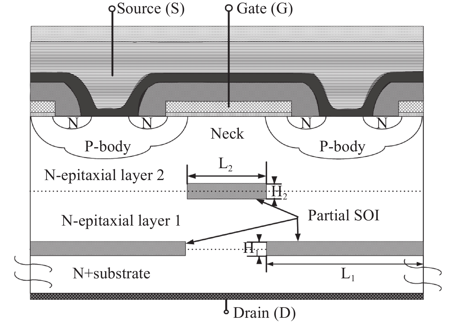
Fig. 1.
Cross section of the proposed VDMOS structure.
SEMICONDUCTOR DEVICES
Zhaohuan Tang1, 2, Xinghua Fu1, , Fashun Yang1, Kaizhou Tan2, Kui Ma1, Xue Wu2 and Jiexing Lin1
Corresponding author: Xinghua Fu, Email: sisc_tang@163.com
Abstract: Single event irradiation-hardened power MOSFET is the most important device for DC/DC converter in space environment application. Single event gate rupture (SEGR) and single event burnout (SEB), which will degrade the running safety and reliability of spacecraft, are the two typical failure modes in power MOSFETs. In this paper, based on recombination mechanism of interface between oxide and silicon, a novel hardened power MOSFETs structure for SEGR and SEB is proposed. The structure comprises double stagger partial silicon-on-insulator (DSPSOI) layers. Results show that the safety operation area (SOA) of a 130 V N-channel power MOSFET in single event irradiation environment is enhanced by up to 50% when the linear-energy-transfer value of heavy ion is a constant of 98 MeV·cm2/mg in the whole incident track, and the other parameters are almost maintained at the same value. Thus this novel structure can be widely used in designing single event irradiation-hardened power MOSFETs.
Keywords: power MOSFETs, partial silicon-on-insulator, single event gate rupture, single event burnout
| [1] |
Sze S M. Physics of semiconductor devices. 2nd ed. Wiley, 1981: 222
|
| [2] |
Johnson G H, Galloway K F, Schrimpf R D, et al. A physical interpretation for the single event gate rupture cross-section of N-channel power MOSFETs. IEEE Trans Nucl Sci, 1996, 43(6): 2932 doi: 10.1109/23.556888
|
| [3] |
Johnson G H, Palau J M, Dachs C, et al. A review of the techniques used for modeling single-event effects in power MOSFETs. IEEE Trans Nucl Sci, 1996, 43(6): 546
|
| [4] |
Sandra L, Jeffery L T, Christopher D, et al. Recommended test conditions for SEB evaluation of planar power DMOSFETs. IEEE Trans Nucl Sci, 2008, 55(6): 3122 doi: 10.1109/TNS.2008.2006841
|
| [5] |
Sandra L, Jeffery L T, Max Z, et al. Worst-Case test conditions of SEGR for power DMOSFETs. IEEE Trans Nucl Sci, 2010, 57(1): 279 doi: 10.1109/TNS.2009.2036614
|
| [6] |
Saburo T, Takashi K, Fumiaki K, et al. Semiconductor device having an SEB voltage suitable for use in space. USA Patent, US6885063 B3, 2005
|
| [7] |
Tang Z H, Hu G Y, Chen G B, et al. A novel structure for improving the SEGR of a VDMOS. J Semicond, 2012, 33(4): 044002 doi: 10.1088/1674-4926/33/4/044002
|
| [8] |
Dumitru S, Marc H V, Eric K. Pseudo self aligend radhard MOSFET and process of manufacture. USA Patent, US0181280 A1, 2013
|
| [9] |
Jia Y P, Su H Y, Jin R, et al. Simulation study on single event burnout in liner doping buffer layer engineered power VDMOSFET. J Semicond, 2016, 37(2): 024008 doi: 10.1088/1674-4926/37/2/024008
|
| [10] |
Jeffery L T. An updated perspective of single event gate rupture and single event burnout in power MOSFETs. IEEE Trans Nucl Sci, 2013, 60(3): 1912 doi: 10.1109/TNS.2013.2252194
|
| [11] |
Li Z H, Zhang Z C, Zhang B, et al. The radiation characteristic of partial SOI VDMOS. International Conference on Communications, Circuits and Systems, 2008: 1361
|
| [12] |
Silvaco Company, Atlas User's Manual.Version W-2013.10, 2013
|
| [13] |
Vladimir V E, Alexander S, Vatuev, et al. New insight into heavy ion induced SEGR impact of charge yield. 15th European Conference on Radiation and Its Effects on Components and Systems, 2015: 1
|
| [14] |
Cheng H Y, Ying W, Fei C, et al. Research of single-event burnout in power planar VDMOSFETs by localized carrier lifetime control. IEEE Trans Nucl Sci, 2014, 62(1): 143
|
| [15] |
Arto J, Veronique F, Alexander B, et al. SEGR in SiO2-SI3N4 Stack. IEEE Trans Nucl Sci, 2014, 61(4):1902 doi: 10.1109/TNS.2014.2303493
|
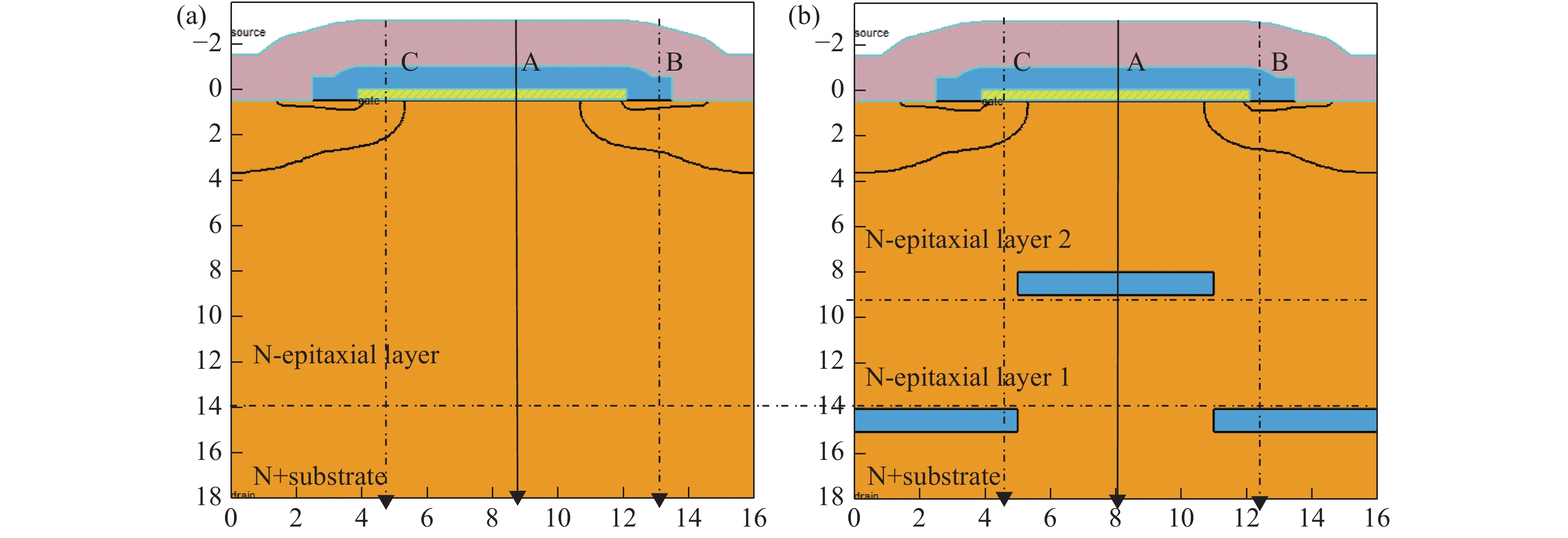
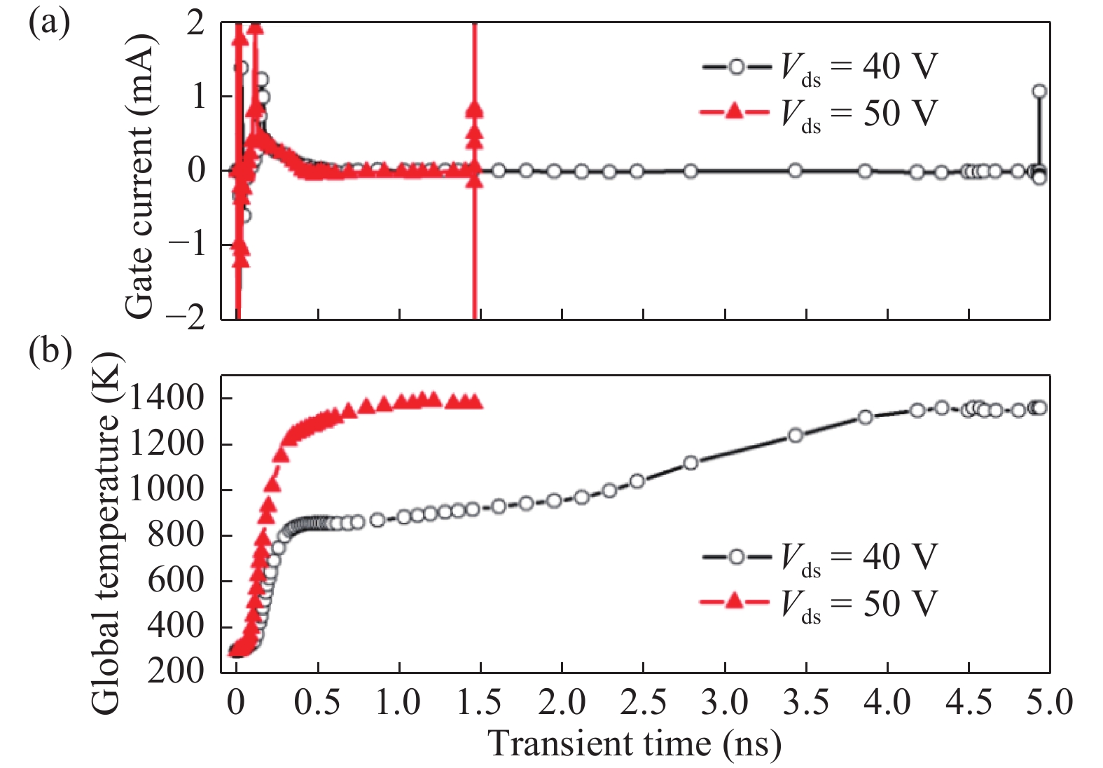
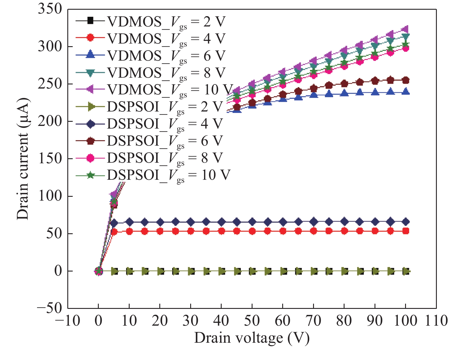
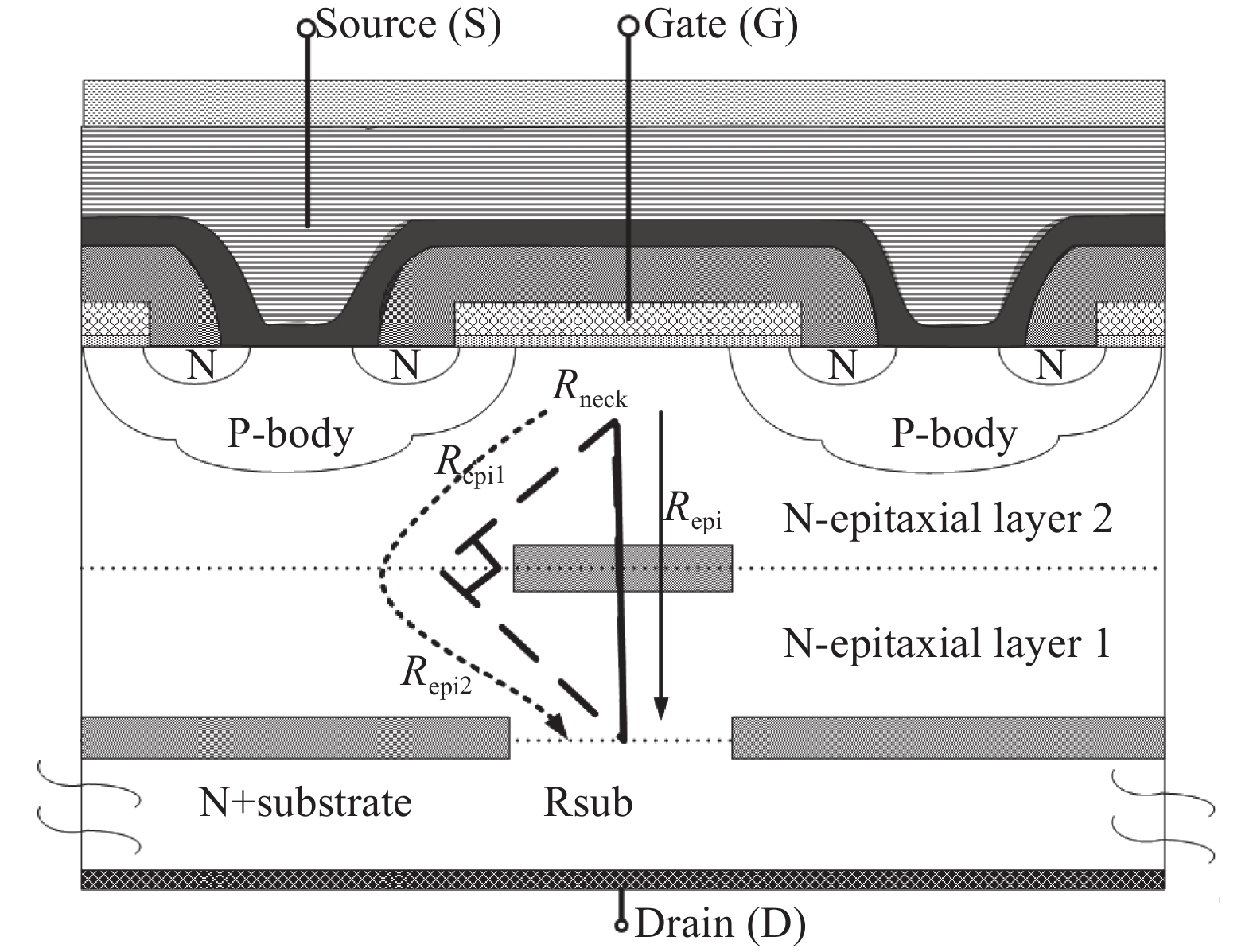
Table 1. The structure and process parameters for a 130 V DSPSOI_MOS.
| Parameters | Conventional MOS | DSPSOI_MOS | Unit |
| Resistivity of epitaxial | 2.4 | / | Ω·cm |
| Resistivity of layer 1 | / | 2.4 | Ω·cm |
| Resistivity of layer 1 | / | 2.4 | Ω·cm |
| L1 length | / | 5 | μm |
| H1 thickness | / | 1 | μm |
| L2 length | / | 6 | μm |
| H2 thickness | / | 1 | μm |
| Epitaxial layer thickness | 14 | / | μm |
| Epitaxial layer 1 thickness | / | 6 | μm |
| Epitaxial layer 2 thickness* | / | 8 | μm |
| P-body junction depth | 3.4 | 3.4 | μm |
| P-body implanting dose | 7 × 10¹³ | 7 × 10¹³ | cm−2 |
| P-body width size | 8 | 8 | μm |
| Poly-silicon width size | 8 | 8 | μm |
| *2 μm is sacrificial layer, and used up in oxidation. | |||
 DownLoad: CSV
Table 2. The simulated DC parameters of the conventional and proposed structures.
| DC parameter | Conventional VDMOS | DSPSOI_MOS |
| Threshold voltage (V) | 2.87 | 2.62 |
| Breakdown voltage (V) | 150.8 | 161.2 |
| Specific on-resistance (mΩ·cm2) | 10.96 | 11.36 |
DownLoad: CSV
| [1] |
Sze S M. Physics of semiconductor devices. 2nd ed. Wiley, 1981: 222
|
| [2] |
Johnson G H, Galloway K F, Schrimpf R D, et al. A physical interpretation for the single event gate rupture cross-section of N-channel power MOSFETs. IEEE Trans Nucl Sci, 1996, 43(6): 2932 doi: 10.1109/23.556888
|
| [3] |
Johnson G H, Palau J M, Dachs C, et al. A review of the techniques used for modeling single-event effects in power MOSFETs. IEEE Trans Nucl Sci, 1996, 43(6): 546
|
| [4] |
Sandra L, Jeffery L T, Christopher D, et al. Recommended test conditions for SEB evaluation of planar power DMOSFETs. IEEE Trans Nucl Sci, 2008, 55(6): 3122 doi: 10.1109/TNS.2008.2006841
|
| [5] |
Sandra L, Jeffery L T, Max Z, et al. Worst-Case test conditions of SEGR for power DMOSFETs. IEEE Trans Nucl Sci, 2010, 57(1): 279 doi: 10.1109/TNS.2009.2036614
|
| [6] |
Saburo T, Takashi K, Fumiaki K, et al. Semiconductor device having an SEB voltage suitable for use in space. USA Patent, US6885063 B3, 2005
|
| [7] |
Tang Z H, Hu G Y, Chen G B, et al. A novel structure for improving the SEGR of a VDMOS. J Semicond, 2012, 33(4): 044002 doi: 10.1088/1674-4926/33/4/044002
|
| [8] |
Dumitru S, Marc H V, Eric K. Pseudo self aligend radhard MOSFET and process of manufacture. USA Patent, US0181280 A1, 2013
|
| [9] |
Jia Y P, Su H Y, Jin R, et al. Simulation study on single event burnout in liner doping buffer layer engineered power VDMOSFET. J Semicond, 2016, 37(2): 024008 doi: 10.1088/1674-4926/37/2/024008
|
| [10] |
Jeffery L T. An updated perspective of single event gate rupture and single event burnout in power MOSFETs. IEEE Trans Nucl Sci, 2013, 60(3): 1912 doi: 10.1109/TNS.2013.2252194
|
| [11] |
Li Z H, Zhang Z C, Zhang B, et al. The radiation characteristic of partial SOI VDMOS. International Conference on Communications, Circuits and Systems, 2008: 1361
|
| [12] |
Silvaco Company, Atlas User's Manual.Version W-2013.10, 2013
|
| [13] |
Vladimir V E, Alexander S, Vatuev, et al. New insight into heavy ion induced SEGR impact of charge yield. 15th European Conference on Radiation and Its Effects on Components and Systems, 2015: 1
|
| [14] |
Cheng H Y, Ying W, Fei C, et al. Research of single-event burnout in power planar VDMOSFETs by localized carrier lifetime control. IEEE Trans Nucl Sci, 2014, 62(1): 143
|
| [15] |
Arto J, Veronique F, Alexander B, et al. SEGR in SiO2-SI3N4 Stack. IEEE Trans Nucl Sci, 2014, 61(4):1902 doi: 10.1109/TNS.2014.2303493
|


Article views: 4290 Times PDF downloads: 70 Times Cited by: 0 Times
Received: 19 April 2017 Revised: 15 June 2017 Online: Corrected proof: 15 November 2017Published: 01 December 2017
| Citation: |
Zhaohuan Tang, Xinghua Fu, Fashun Yang, Kaizhou Tan, Kui Ma, Xue Wu, Jiexing Lin. SEGR- and SEB-hardened structure with DSPSOI in power MOSFETs[J]. Journal of Semiconductors, 2017, 38(12): 124006. doi: 10.1088/1674-4926/38/12/124006
****
Z H Tang, X H Fu, F S Yang, K Z Tan, K Ma, X Wu, J X Lin. SEGR- and SEB-hardened structure with DSPSOI in power MOSFETs[J]. J. Semicond., 2017, 38(12): 124006. doi: 10.1088/1674-4926/38/12/124006.

|
| [1] |
Sze S M. Physics of semiconductor devices. 2nd ed. Wiley, 1981: 222
|
| [2] |
Johnson G H, Galloway K F, Schrimpf R D, et al. A physical interpretation for the single event gate rupture cross-section of N-channel power MOSFETs. IEEE Trans Nucl Sci, 1996, 43(6): 2932 doi: 10.1109/23.556888
|
| [3] |
Johnson G H, Palau J M, Dachs C, et al. A review of the techniques used for modeling single-event effects in power MOSFETs. IEEE Trans Nucl Sci, 1996, 43(6): 546
|
| [4] |
Sandra L, Jeffery L T, Christopher D, et al. Recommended test conditions for SEB evaluation of planar power DMOSFETs. IEEE Trans Nucl Sci, 2008, 55(6): 3122 doi: 10.1109/TNS.2008.2006841
|
| [5] |
Sandra L, Jeffery L T, Max Z, et al. Worst-Case test conditions of SEGR for power DMOSFETs. IEEE Trans Nucl Sci, 2010, 57(1): 279 doi: 10.1109/TNS.2009.2036614
|
| [6] |
Saburo T, Takashi K, Fumiaki K, et al. Semiconductor device having an SEB voltage suitable for use in space. USA Patent, US6885063 B3, 2005
|
| [7] |
Tang Z H, Hu G Y, Chen G B, et al. A novel structure for improving the SEGR of a VDMOS. J Semicond, 2012, 33(4): 044002 doi: 10.1088/1674-4926/33/4/044002
|
| [8] |
Dumitru S, Marc H V, Eric K. Pseudo self aligend radhard MOSFET and process of manufacture. USA Patent, US0181280 A1, 2013
|
| [9] |
Jia Y P, Su H Y, Jin R, et al. Simulation study on single event burnout in liner doping buffer layer engineered power VDMOSFET. J Semicond, 2016, 37(2): 024008 doi: 10.1088/1674-4926/37/2/024008
|
| [10] |
Jeffery L T. An updated perspective of single event gate rupture and single event burnout in power MOSFETs. IEEE Trans Nucl Sci, 2013, 60(3): 1912 doi: 10.1109/TNS.2013.2252194
|
| [11] |
Li Z H, Zhang Z C, Zhang B, et al. The radiation characteristic of partial SOI VDMOS. International Conference on Communications, Circuits and Systems, 2008: 1361
|
| [12] |
Silvaco Company, Atlas User's Manual.Version W-2013.10, 2013
|
| [13] |
Vladimir V E, Alexander S, Vatuev, et al. New insight into heavy ion induced SEGR impact of charge yield. 15th European Conference on Radiation and Its Effects on Components and Systems, 2015: 1
|
| [14] |
Cheng H Y, Ying W, Fei C, et al. Research of single-event burnout in power planar VDMOSFETs by localized carrier lifetime control. IEEE Trans Nucl Sci, 2014, 62(1): 143
|
| [15] |
Arto J, Veronique F, Alexander B, et al. SEGR in SiO2-SI3N4 Stack. IEEE Trans Nucl Sci, 2014, 61(4):1902 doi: 10.1109/TNS.2014.2303493
|

 WeChat ID
Journal of Semiconductors © 2017 All Rights Reserved 京ICP备05085259号-2


