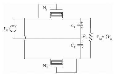
Fig. 1.
Wireless power transmission system for implantable applications.
SEMICONDUCTOR INTEGRATED CIRCUITS
Yonggen Tu, Libo Qian and Yinshui Xia
Corresponding author: Libo Qian, Email:qianlibo@nbu.edu.cn
Abstract: Carbon nanotube field effect transistor (CNFET) shows lower threshold voltage and smaller leakage current in comparison to its CMOS counterpart. In this paper, two kinds of CNFET-based rectifiers, full-wave rectifiers and voltage doubler rectifiers are presented for biomedical implantable applications. Based on the standard 32 nm CNFET model, the electrical performance of CNFET rectifiers is analyzed and compared. Simulation results show the voltage conversion efficiency (VCE) and power conversion efficiency (PCE) achieve 70.82% and 72.49% for CNFET full-wave rectifiers and 56.60% and 61.17% for CNFET voltage double rectifiers at typical 1.0 V input voltage excitation, which are higher than that of CMOS design. Moreover, considering the controllable property of CNFET threshold voltage, the effect of various design parameters on the electrical performance is investigated. It is observed that the VCE and PCE of CNFET rectifier increase with increasing CNT diameter and number of tubes. The proposed results would provide some guidelines for design and optimization of CNFET-based rectifier circuits.
Keywords: CNFET technology, rectifier, power conversion efficiency, biomedical implantable applications
| [1] |
Weir R F, Troyk P R, DeMichele G A, et al. Implantable myelectric sensors (IMESs) for intramuscular electromyogram recording. IEEE Trans Biomed Eng, 2009, 56(1):159. doi: 10.1109/TBME.2008.2005942
|
| [2] |
Benoit G, Amer E, Ayoub, et al. A mix-signal multichip neural recording interface with bandwidth reduction. IEEE Trans Biomed Circuits Syst, 2009, 3(3):129 doi: 10.1109/TBCAS.2009.2013718
|
| [3] |
Shao H X, Wu J F, Han Z S, et al. Thin film thickness effect on 0.1μm dimension SOI Groove gate device characteristics. Microelectron Comput, 2006, 23(05):28
|
| [4] |
Qian L B, Xia Y S, Shi G. Electrical modeling and analysis of a mixed carbon nanotube based differential through silicon via in 3-D integration. IEEE Trans Nanotechnol, 2016, 15(2):155 doi: 10.1109/TNANO.2015.2509019
|
| [5] |
Sankar P A, Udhayakumar K. MOSFET-like CNFET based login gate library for low-power application:a comparative study. J Semicond, 2014, 35(7):075001 doi: 10.1088/1674-4926/35/7/075001
|
| [6] |
Dürkop T, Getty S A, Cobas E, et al. Extraordinary mobility in semiconducting carbon nanotubes. Nano Lett, 2004, 4(1):35 doi: 10.1021/nl034841q
|
| [7] |
Zhang Z Y, Wang S, Peng L M. High-performance doping-free carbon-nanotube-based CMOS devices and integrated circuits. Chin Sci Bull, 2012, 57:135 doi: 10.1007/s11434-011-4791-6
|
| [8] |
Chen Z. H, Farmer D, Xu S, et al. Externally assembled gateall-around carbon nanotube field-effect transistor. IEEE Electron Device Lett, 2008, 29(2):183 doi: 10.1109/LED.2007.914069
|
| [9] |
Xu G B, Chen X, Zhou Q, et al. Design and application of carbon nanotube FETs. J Electron Meas Instrum, 2010, 24(10):969 doi: 10.3724/SP.J.1187.2010.00969
|
| [10] |
Puri A, Rana A. Performance analysis of CNTFET based low power operational amplifier in analog circuits for biomedical applications. IEEE International Conference on Electronics, Computing and Communication Technologies, 2015:1 https://www.researchgate.net/publication/302479599_Performance_analysis_of_CNTFET_based_low_power_operational_amplifier_in_analog_circuits_for_biomedical_applications
|
| [11] |
Tyagi A, Gopi C, Baldi P, et al. CNFET-based 0.1 to 1.2 V DC/DC boost converters with voltage regulation for energy harvesting applications. IEEE Trans Nanotechnol, 2015, 14(4):660 doi: 10.1109/TNANO.2015.2427292
|
| [12] |
Wang J M, Yang Z, Zhu Z M, et al. An ultra-low voltage rectifier for PE energy harvesting applications. J Semicond, 2016, 37(2):025004 doi: 10.1088/1674-4926/37/2/025004
|
| [13] |
Tyagi A, Gopi C, Baldi P, et al. CNFET-based 0.1 V to 0.6 V DC/DC converters. Recent Advances in Engineering and Computational Sciences (RAECS), 2015:1
|
| [14] |
Raychowdhury A, Roy K. Carbon-nanotube-based voltage mode multiple-valued logic design. IEEE Trans Nanotechnol, 2005, 4(2):168 doi: 10.1109/TNANO.2004.842068
|
| [15] |
Ahmed E N, Ahmed M, Anass W, et al. Comparative review of carbon nanotube FETs. 2016 Third International Conference on Electrical, Electronics, Computer Engineering and Their Applications (EECEA), 2016:57
|
| [16] |
Akinwande D, Liang J, Chang S, et al. Analytical ballistic theory of carbon nanotube transistors:experimental validation, device physics, parameter extraction, and performance projections. J Appl Phys, 2008, 104:124514 doi: 10.1063/1.3050345
|
| [17] |
Berkeley predictive technology model. http://ptm.asu.edu/
|
| [18] |
Sinha S K, Chaudhury S. Comparative study of leakage power in CNTFET over MOSFET device. J Semicond, 2014, 35(11):114002 doi: 10.1088/1674-4926/35/11/114002
|
| [19] |
Lin A, Patil N, Ryu K, et al. Threshold voltage and on-off ratio tuning for multiple tube carbon nanotube FETs. IEEE Trans Nanotechnol, 2009, 8(1):4 doi: 10.1109/TNANO.2008.2004706
|
| [20] |
Stanford University CNFET model. http://nano.stanford.edu/model/php?idD23
|
| [21] |
Akinwande D, Close G F, Wong H S. Analysis of the frequency response of carbon nanotube transistors. IEEE Trans Nanotechnol, 2006, 5:599 doi: 10.1109/TNANO.2006.880451
|
| [22] |
Amlani I, Lee K. F, Deng J, et al. Measuring frequency response of a single-walled carbon nanotube common-source amplifier. IEEE Trans Nanotechnol, 2009, 8(2):226 doi: 10.1109/TNANO.2008.2010883
|
| [23] |
Singh A, Saini D K, Agarwal D. Modeling and simulation of carbon nanotube field effect transistor and its circuit application. J Semicond, 2016, 37(7):074001 doi: 10.1088/1674-4926/37/7/074001
|
| [24] |
Lin S, Kin Y B, Lombardi F. CNTFET-based design of ternary logic gate and arithmetic circuits. IEEE Trans Nanotechnol, 2011, 10(2):217 doi: 10.1109/TNANO.2009.2036845
|
| [25] |
Bi X W, Liang H L, Gu X F, et al. Design of novel DDSCR with embedded PNP structure for ESD protection. J Semicond, 2015, 36(12):124007 doi: 10.1088/1674-4926/36/12/124007
|
| [26] |
Wang F J, Zhu Z M, Yang Y T, et al. A effective approach of reducing the keep out zone (KOZ) induced by coaxial through silicon via (TSV). IEEE Trans Electron Device, 2014, 61(8):2928 doi: 10.1109/TED.2014.2330838
|
| [27] |
Deng J, Wong H S P. A compact SPICE model for carbon nanotube field effect transistors including nonidealities and its application-Part I:model of the intrinsic channel region. IEEE Trans Electron Devices, 2007, 54(12):3186 doi: 10.1109/TED.2007.909030
|
| [28] |
Deng J, Wong H S P. A compact SPICE model for carbon nanotube field effect transistors including nonidealities and its application-Part Ⅱ:full device model and circuit performance benchmarking. IEEE Trans Electron Devices, 2007, 54(12):3195 doi: 10.1109/TED.2007.909043
|
| [29] |
Deng J, Patil N, Ryu K, et al. Carbon nanotube transistor circuits:circuit-level performance benchmarking and design options for living with imperfections. International Solid State Circuits Conference (ISSCC), San Francisco, 2007:70 https://www.researchgate.net/publication/4255329_Carbon_Nanotube_Transistor_Circuits_Circuit-Level_Performance_Benchmarking_and_Design_Options_for_Living_with_Imperfections?_sg=9b42KKF0k3Ja7W0MuZG7JcupeL2vULPzRwvj_X-mAx52BJoAZEB5f0KuJtB9rqmXv-9Vk33FRmhPn1PwVQChnw
|
| [30] |
Luo J, Wei L, Lee C S. Compact model for carbon nanotube field effect transistors including nonidealities and calibrated with experimental data down to 9 nm gate length. IEEE Trans Electron Devices, 2013, 60(6):1834 doi: 10.1109/TED.2013.2258023
|
| [31] |
Shi J H, Zhao T, Li X C. First principles of calculation on electronic properties of B and N co-doping carbon nanotube. J Semicond, 2016, 37(3):032002 doi: 10.1088/1674-4926/37/3/032002
|
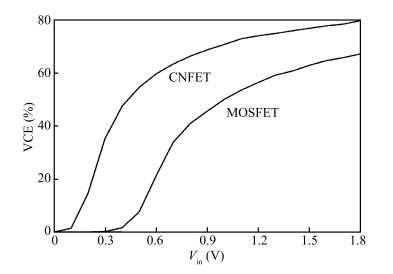
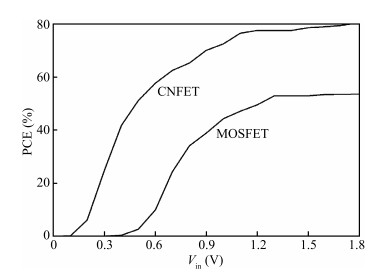
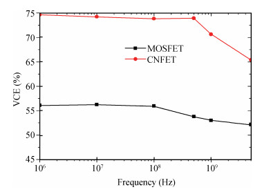
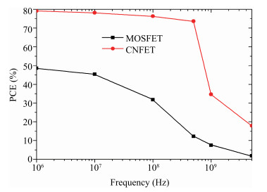
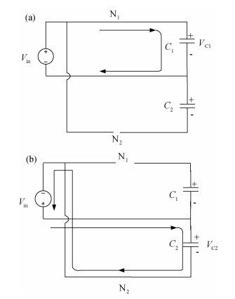
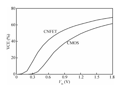
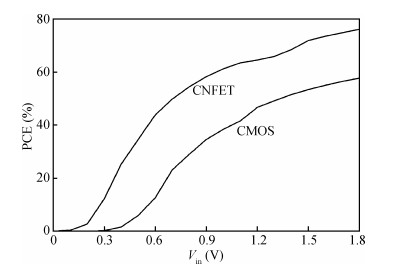
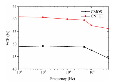
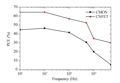
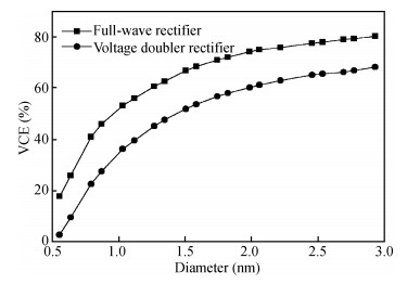
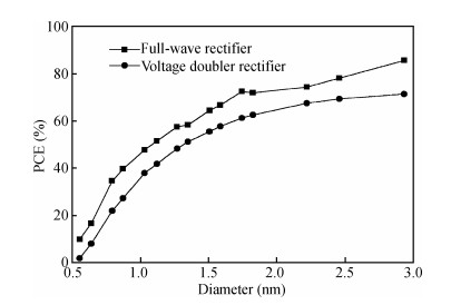
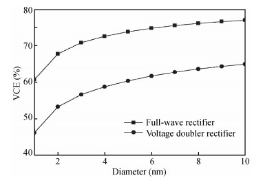
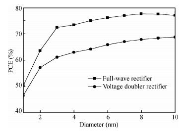
Table 1. Threshold voltage of FETs at different technology nodes

|
Table 2. Baseline design parameters of CNFET

|
| [1] |
Weir R F, Troyk P R, DeMichele G A, et al. Implantable myelectric sensors (IMESs) for intramuscular electromyogram recording. IEEE Trans Biomed Eng, 2009, 56(1):159. doi: 10.1109/TBME.2008.2005942
|
| [2] |
Benoit G, Amer E, Ayoub, et al. A mix-signal multichip neural recording interface with bandwidth reduction. IEEE Trans Biomed Circuits Syst, 2009, 3(3):129 doi: 10.1109/TBCAS.2009.2013718
|
| [3] |
Shao H X, Wu J F, Han Z S, et al. Thin film thickness effect on 0.1μm dimension SOI Groove gate device characteristics. Microelectron Comput, 2006, 23(05):28
|
| [4] |
Qian L B, Xia Y S, Shi G. Electrical modeling and analysis of a mixed carbon nanotube based differential through silicon via in 3-D integration. IEEE Trans Nanotechnol, 2016, 15(2):155 doi: 10.1109/TNANO.2015.2509019
|
| [5] |
Sankar P A, Udhayakumar K. MOSFET-like CNFET based login gate library for low-power application:a comparative study. J Semicond, 2014, 35(7):075001 doi: 10.1088/1674-4926/35/7/075001
|
| [6] |
Dürkop T, Getty S A, Cobas E, et al. Extraordinary mobility in semiconducting carbon nanotubes. Nano Lett, 2004, 4(1):35 doi: 10.1021/nl034841q
|
| [7] |
Zhang Z Y, Wang S, Peng L M. High-performance doping-free carbon-nanotube-based CMOS devices and integrated circuits. Chin Sci Bull, 2012, 57:135 doi: 10.1007/s11434-011-4791-6
|
| [8] |
Chen Z. H, Farmer D, Xu S, et al. Externally assembled gateall-around carbon nanotube field-effect transistor. IEEE Electron Device Lett, 2008, 29(2):183 doi: 10.1109/LED.2007.914069
|
| [9] |
Xu G B, Chen X, Zhou Q, et al. Design and application of carbon nanotube FETs. J Electron Meas Instrum, 2010, 24(10):969 doi: 10.3724/SP.J.1187.2010.00969
|
| [10] |
Puri A, Rana A. Performance analysis of CNTFET based low power operational amplifier in analog circuits for biomedical applications. IEEE International Conference on Electronics, Computing and Communication Technologies, 2015:1 https://www.researchgate.net/publication/302479599_Performance_analysis_of_CNTFET_based_low_power_operational_amplifier_in_analog_circuits_for_biomedical_applications
|
| [11] |
Tyagi A, Gopi C, Baldi P, et al. CNFET-based 0.1 to 1.2 V DC/DC boost converters with voltage regulation for energy harvesting applications. IEEE Trans Nanotechnol, 2015, 14(4):660 doi: 10.1109/TNANO.2015.2427292
|
| [12] |
Wang J M, Yang Z, Zhu Z M, et al. An ultra-low voltage rectifier for PE energy harvesting applications. J Semicond, 2016, 37(2):025004 doi: 10.1088/1674-4926/37/2/025004
|
| [13] |
Tyagi A, Gopi C, Baldi P, et al. CNFET-based 0.1 V to 0.6 V DC/DC converters. Recent Advances in Engineering and Computational Sciences (RAECS), 2015:1
|
| [14] |
Raychowdhury A, Roy K. Carbon-nanotube-based voltage mode multiple-valued logic design. IEEE Trans Nanotechnol, 2005, 4(2):168 doi: 10.1109/TNANO.2004.842068
|
| [15] |
Ahmed E N, Ahmed M, Anass W, et al. Comparative review of carbon nanotube FETs. 2016 Third International Conference on Electrical, Electronics, Computer Engineering and Their Applications (EECEA), 2016:57
|
| [16] |
Akinwande D, Liang J, Chang S, et al. Analytical ballistic theory of carbon nanotube transistors:experimental validation, device physics, parameter extraction, and performance projections. J Appl Phys, 2008, 104:124514 doi: 10.1063/1.3050345
|
| [17] |
Berkeley predictive technology model. http://ptm.asu.edu/
|
| [18] |
Sinha S K, Chaudhury S. Comparative study of leakage power in CNTFET over MOSFET device. J Semicond, 2014, 35(11):114002 doi: 10.1088/1674-4926/35/11/114002
|
| [19] |
Lin A, Patil N, Ryu K, et al. Threshold voltage and on-off ratio tuning for multiple tube carbon nanotube FETs. IEEE Trans Nanotechnol, 2009, 8(1):4 doi: 10.1109/TNANO.2008.2004706
|
| [20] |
Stanford University CNFET model. http://nano.stanford.edu/model/php?idD23
|
| [21] |
Akinwande D, Close G F, Wong H S. Analysis of the frequency response of carbon nanotube transistors. IEEE Trans Nanotechnol, 2006, 5:599 doi: 10.1109/TNANO.2006.880451
|
| [22] |
Amlani I, Lee K. F, Deng J, et al. Measuring frequency response of a single-walled carbon nanotube common-source amplifier. IEEE Trans Nanotechnol, 2009, 8(2):226 doi: 10.1109/TNANO.2008.2010883
|
| [23] |
Singh A, Saini D K, Agarwal D. Modeling and simulation of carbon nanotube field effect transistor and its circuit application. J Semicond, 2016, 37(7):074001 doi: 10.1088/1674-4926/37/7/074001
|
| [24] |
Lin S, Kin Y B, Lombardi F. CNTFET-based design of ternary logic gate and arithmetic circuits. IEEE Trans Nanotechnol, 2011, 10(2):217 doi: 10.1109/TNANO.2009.2036845
|
| [25] |
Bi X W, Liang H L, Gu X F, et al. Design of novel DDSCR with embedded PNP structure for ESD protection. J Semicond, 2015, 36(12):124007 doi: 10.1088/1674-4926/36/12/124007
|
| [26] |
Wang F J, Zhu Z M, Yang Y T, et al. A effective approach of reducing the keep out zone (KOZ) induced by coaxial through silicon via (TSV). IEEE Trans Electron Device, 2014, 61(8):2928 doi: 10.1109/TED.2014.2330838
|
| [27] |
Deng J, Wong H S P. A compact SPICE model for carbon nanotube field effect transistors including nonidealities and its application-Part I:model of the intrinsic channel region. IEEE Trans Electron Devices, 2007, 54(12):3186 doi: 10.1109/TED.2007.909030
|
| [28] |
Deng J, Wong H S P. A compact SPICE model for carbon nanotube field effect transistors including nonidealities and its application-Part Ⅱ:full device model and circuit performance benchmarking. IEEE Trans Electron Devices, 2007, 54(12):3195 doi: 10.1109/TED.2007.909043
|
| [29] |
Deng J, Patil N, Ryu K, et al. Carbon nanotube transistor circuits:circuit-level performance benchmarking and design options for living with imperfections. International Solid State Circuits Conference (ISSCC), San Francisco, 2007:70 https://www.researchgate.net/publication/4255329_Carbon_Nanotube_Transistor_Circuits_Circuit-Level_Performance_Benchmarking_and_Design_Options_for_Living_with_Imperfections?_sg=9b42KKF0k3Ja7W0MuZG7JcupeL2vULPzRwvj_X-mAx52BJoAZEB5f0KuJtB9rqmXv-9Vk33FRmhPn1PwVQChnw
|
| [30] |
Luo J, Wei L, Lee C S. Compact model for carbon nanotube field effect transistors including nonidealities and calibrated with experimental data down to 9 nm gate length. IEEE Trans Electron Devices, 2013, 60(6):1834 doi: 10.1109/TED.2013.2258023
|
| [31] |
Shi J H, Zhao T, Li X C. First principles of calculation on electronic properties of B and N co-doping carbon nanotube. J Semicond, 2016, 37(3):032002 doi: 10.1088/1674-4926/37/3/032002
|


Article views: 3412 Times PDF downloads: 33 Times Cited by: 0 Times
Received: 20 June 2016 Revised: 18 August 2016 Online: Published: 01 February 2017
| Citation: |
Yonggen Tu, Libo Qian, Yinshui Xia. CNFET-based voltage rectifier circuit for biomedical implantable applications[J]. Journal of Semiconductors, 2017, 38(2): 025003. doi: 10.1088/1674-4926/38/2/025003
****
Y G Tu, L B Qian, Y S Xia. CNFET-based voltage rectifier circuit for biomedical implantable applications[J]. J. Semicond., 2017, 38(2): 025003. doi: 10.1088/1674-4926/38/2/025003.

|
| [1] |
Weir R F, Troyk P R, DeMichele G A, et al. Implantable myelectric sensors (IMESs) for intramuscular electromyogram recording. IEEE Trans Biomed Eng, 2009, 56(1):159. doi: 10.1109/TBME.2008.2005942
|
| [2] |
Benoit G, Amer E, Ayoub, et al. A mix-signal multichip neural recording interface with bandwidth reduction. IEEE Trans Biomed Circuits Syst, 2009, 3(3):129 doi: 10.1109/TBCAS.2009.2013718
|
| [3] |
Shao H X, Wu J F, Han Z S, et al. Thin film thickness effect on 0.1μm dimension SOI Groove gate device characteristics. Microelectron Comput, 2006, 23(05):28
|
| [4] |
Qian L B, Xia Y S, Shi G. Electrical modeling and analysis of a mixed carbon nanotube based differential through silicon via in 3-D integration. IEEE Trans Nanotechnol, 2016, 15(2):155 doi: 10.1109/TNANO.2015.2509019
|
| [5] |
Sankar P A, Udhayakumar K. MOSFET-like CNFET based login gate library for low-power application:a comparative study. J Semicond, 2014, 35(7):075001 doi: 10.1088/1674-4926/35/7/075001
|
| [6] |
Dürkop T, Getty S A, Cobas E, et al. Extraordinary mobility in semiconducting carbon nanotubes. Nano Lett, 2004, 4(1):35 doi: 10.1021/nl034841q
|
| [7] |
Zhang Z Y, Wang S, Peng L M. High-performance doping-free carbon-nanotube-based CMOS devices and integrated circuits. Chin Sci Bull, 2012, 57:135 doi: 10.1007/s11434-011-4791-6
|
| [8] |
Chen Z. H, Farmer D, Xu S, et al. Externally assembled gateall-around carbon nanotube field-effect transistor. IEEE Electron Device Lett, 2008, 29(2):183 doi: 10.1109/LED.2007.914069
|
| [9] |
Xu G B, Chen X, Zhou Q, et al. Design and application of carbon nanotube FETs. J Electron Meas Instrum, 2010, 24(10):969 doi: 10.3724/SP.J.1187.2010.00969
|
| [10] |
Puri A, Rana A. Performance analysis of CNTFET based low power operational amplifier in analog circuits for biomedical applications. IEEE International Conference on Electronics, Computing and Communication Technologies, 2015:1 https://www.researchgate.net/publication/302479599_Performance_analysis_of_CNTFET_based_low_power_operational_amplifier_in_analog_circuits_for_biomedical_applications
|
| [11] |
Tyagi A, Gopi C, Baldi P, et al. CNFET-based 0.1 to 1.2 V DC/DC boost converters with voltage regulation for energy harvesting applications. IEEE Trans Nanotechnol, 2015, 14(4):660 doi: 10.1109/TNANO.2015.2427292
|
| [12] |
Wang J M, Yang Z, Zhu Z M, et al. An ultra-low voltage rectifier for PE energy harvesting applications. J Semicond, 2016, 37(2):025004 doi: 10.1088/1674-4926/37/2/025004
|
| [13] |
Tyagi A, Gopi C, Baldi P, et al. CNFET-based 0.1 V to 0.6 V DC/DC converters. Recent Advances in Engineering and Computational Sciences (RAECS), 2015:1
|
| [14] |
Raychowdhury A, Roy K. Carbon-nanotube-based voltage mode multiple-valued logic design. IEEE Trans Nanotechnol, 2005, 4(2):168 doi: 10.1109/TNANO.2004.842068
|
| [15] |
Ahmed E N, Ahmed M, Anass W, et al. Comparative review of carbon nanotube FETs. 2016 Third International Conference on Electrical, Electronics, Computer Engineering and Their Applications (EECEA), 2016:57
|
| [16] |
Akinwande D, Liang J, Chang S, et al. Analytical ballistic theory of carbon nanotube transistors:experimental validation, device physics, parameter extraction, and performance projections. J Appl Phys, 2008, 104:124514 doi: 10.1063/1.3050345
|
| [17] |
Berkeley predictive technology model. http://ptm.asu.edu/
|
| [18] |
Sinha S K, Chaudhury S. Comparative study of leakage power in CNTFET over MOSFET device. J Semicond, 2014, 35(11):114002 doi: 10.1088/1674-4926/35/11/114002
|
| [19] |
Lin A, Patil N, Ryu K, et al. Threshold voltage and on-off ratio tuning for multiple tube carbon nanotube FETs. IEEE Trans Nanotechnol, 2009, 8(1):4 doi: 10.1109/TNANO.2008.2004706
|
| [20] |
Stanford University CNFET model. http://nano.stanford.edu/model/php?idD23
|
| [21] |
Akinwande D, Close G F, Wong H S. Analysis of the frequency response of carbon nanotube transistors. IEEE Trans Nanotechnol, 2006, 5:599 doi: 10.1109/TNANO.2006.880451
|
| [22] |
Amlani I, Lee K. F, Deng J, et al. Measuring frequency response of a single-walled carbon nanotube common-source amplifier. IEEE Trans Nanotechnol, 2009, 8(2):226 doi: 10.1109/TNANO.2008.2010883
|
| [23] |
Singh A, Saini D K, Agarwal D. Modeling and simulation of carbon nanotube field effect transistor and its circuit application. J Semicond, 2016, 37(7):074001 doi: 10.1088/1674-4926/37/7/074001
|
| [24] |
Lin S, Kin Y B, Lombardi F. CNTFET-based design of ternary logic gate and arithmetic circuits. IEEE Trans Nanotechnol, 2011, 10(2):217 doi: 10.1109/TNANO.2009.2036845
|
| [25] |
Bi X W, Liang H L, Gu X F, et al. Design of novel DDSCR with embedded PNP structure for ESD protection. J Semicond, 2015, 36(12):124007 doi: 10.1088/1674-4926/36/12/124007
|
| [26] |
Wang F J, Zhu Z M, Yang Y T, et al. A effective approach of reducing the keep out zone (KOZ) induced by coaxial through silicon via (TSV). IEEE Trans Electron Device, 2014, 61(8):2928 doi: 10.1109/TED.2014.2330838
|
| [27] |
Deng J, Wong H S P. A compact SPICE model for carbon nanotube field effect transistors including nonidealities and its application-Part I:model of the intrinsic channel region. IEEE Trans Electron Devices, 2007, 54(12):3186 doi: 10.1109/TED.2007.909030
|
| [28] |
Deng J, Wong H S P. A compact SPICE model for carbon nanotube field effect transistors including nonidealities and its application-Part Ⅱ:full device model and circuit performance benchmarking. IEEE Trans Electron Devices, 2007, 54(12):3195 doi: 10.1109/TED.2007.909043
|
| [29] |
Deng J, Patil N, Ryu K, et al. Carbon nanotube transistor circuits:circuit-level performance benchmarking and design options for living with imperfections. International Solid State Circuits Conference (ISSCC), San Francisco, 2007:70 https://www.researchgate.net/publication/4255329_Carbon_Nanotube_Transistor_Circuits_Circuit-Level_Performance_Benchmarking_and_Design_Options_for_Living_with_Imperfections?_sg=9b42KKF0k3Ja7W0MuZG7JcupeL2vULPzRwvj_X-mAx52BJoAZEB5f0KuJtB9rqmXv-9Vk33FRmhPn1PwVQChnw
|
| [30] |
Luo J, Wei L, Lee C S. Compact model for carbon nanotube field effect transistors including nonidealities and calibrated with experimental data down to 9 nm gate length. IEEE Trans Electron Devices, 2013, 60(6):1834 doi: 10.1109/TED.2013.2258023
|
| [31] |
Shi J H, Zhao T, Li X C. First principles of calculation on electronic properties of B and N co-doping carbon nanotube. J Semicond, 2016, 37(3):032002 doi: 10.1088/1674-4926/37/3/032002
|

 WeChat ID
Journal of Semiconductors © 2017 All Rights Reserved 京ICP备05085259号-2

 DownLoad: