J. Semicond. > 2017, Volume 38 > Issue 3 > 031003

SPECIAL TOPIC ON 2D MATERIALS AND DEVICES

Recent progress in synthesis of two-dimensional hexagonal boron nitride

Haolin Wang1, 2, Yajuan Zhao3, Yong Xie1, Xiaohua Ma1 and Xingwang Zhang2,

+ Author Affiliations

 Corresponding author: Xingwang Zhang,Email:xwzhang@semi.ac.cn

DOI: 10.1088/1674-4926/38/3/031003

PDF

Abstract: Two-dimensional (2D) materials have recently received a great deal of attention due to their unique structures and fascinating properties, as well as their potential applications. 2D hexagonal boron nitride (2D h-BN), an insulator with excellent thermal stability, chemical inertness, and unique electronic and optical properties, and a band gap of 5.97 eV, is considered to be an ideal candidate for integration with other 2D materials. Nevertheless, the controllable growth of high-quality 2D h-BN is still a great challenge. A comprehensive overview of the progress that has been made in the synthesis of 2D h-BN is presented, highlighting the advantages and disadvantages of various synthesis approaches. In addition, the electronic, optical, thermal, and mechanical properties, heterostructures, and related applications of 2D h-BN are discussed.

Key words: hexagonal boron nitridetwo-dimensional materialsapplicationssynthesis


[1]
Ferrari A C, Bonaccorso F, Fal'ko V, et al. Science and technology roadmap for graphene, related two-dimensional crystals, and hybrid systems. Nanoscale, 2015, 7(11):4598 doi: 10.1039/C4NR01600A
[2]
Geim A K, Novoselov K S. The rise of graphene. Nat Mater, 2007, 6(3):183 doi: 10.1038/nmat1849
[3]
Zhang H. Ultrathin two-dimensional nanomaterials. ACS Nano, 2015, 9(10):9451 doi: 10.1021/acsnano.5b05040
[4]
Bhimanapati G R, Lin Z, Meunier V. Recent advances in twodimensional materials beyond graphene. ACS Nano, 2015, 9(12):11509 doi: 10.1021/acsnano.5b05556
[5]
Yin J, Li J, Hang Y, et al. Boron nitride nanostructures:fabrication, functionalization and applications. Small, 2016, 12(22):2942 doi: 10.1002/smll.201600053
[6]
Golberg D, Bando Y, Huang Y, et al. Boron nitride nanotubes and nanosheets. ACS Nano, 2010, 4(6):2979 doi: 10.1021/nn1006495
[7]
Pakdel A, Bando Y, Golberg D. Nano boron nitride flatland. Chem Soc Rev, 2014, 43(3):934 doi: 10.1039/C3CS60260E
[8]
Kubota Y, Watanabe K, Tsuda O, et al. Deep ultraviolet lightemitting hexagonal boron nitride synthesized at atmospheric pressure. Science, 2007, 317(5840):932 doi: 10.1126/science.1144216
[9]
Lee K H, Shin H J, Lee J, et al. Large-scale synthesis of high-quality hexagonal boron nitride nanosheets for large-area graphene electronics. Nano Lett, 2012, 12(2):714 doi: 10.1021/nl203635v
[10]
Giovannetti G, Khomyakov P, Brocks G, et al. Substrate induced band gap in graphene on hexagonal boron nitride:ab initio density functional calculations. Phys Rev B, 2007, 76(7):073103 doi: 10.1103/PhysRevB.76.073103
[11]
Dean C R, Young A F, Meric I, et al. Boron nitride substrates for high-quality graphene electronics. Nat Nanotechnol, 2010, 5(10):722 doi: 10.1038/nnano.2010.172
[12]
Mayorov A S, Gorbachev R V, Morozov S V, et al, Micrometerscale ballistic transport in encapsulated graphene at room temperature. Nano Lett, 2011, 11(6):2396 doi: 10.1021/nl200758b
[13]
Yang W, Chen G R, Shi Z W, et al. Epitaxial growth of singledomain graphene on hexagonal boron nitride. Nat Mater, 2013, 12(9):792 doi: 10.1038/nmat3695
[14]
Gibb A L, Alem N, Chen J H, et al. Atomic resolution imaging of grain boundary defects in monolayer chemical vapor depositiongrown hexagonal boron nitride. J Am Chem Soc, 2013, 135(18):6758 doi: 10.1021/ja400637n
[15]
Cretu O, Lin Y C, Suenaga K. Evidence for active atomic defects in monolayer hexagonal boron nitride:a new mechanism of plasticity in two-dimensional materials. Nano Lett, 2014, 14(2):1064 doi: 10.1021/nl404735w
[16]
Bresnehan M S, Hollander M J, Wetherington M, et al. Integration of hexagonal boron nitride with quasi-freestanding epitaxial graphene:toward wafer-scale, high-performance devices. ACS Nano, 2012, 6(6):5234 doi: 10.1021/nn300996t
[17]
Britnell L, Gorbachev R V, Jalil R, et al. Field-effect tunneling transistor based on vertical graphene heterostructures. Science, 2012, 335(6071):947 doi: 10.1126/science.1218461
[18]
Wang J, Yao Q, Huang C W, et al. High mobility MoS2 transistor with low Schottky barrier contact by using atomic thick h-BN as a tunneling layer. Adv Mater, 2016, 28(37):8302 doi: 10.1002/adma.v28.37
[19]
Meng J H, Liu X, Zhang X W, et al. Interface engineering for highly efficient graphene-on-silicon Schottky junction solar cells by introducing a hexagonal boron nitride interlayer. Nano Energy, 2016, 28:44 doi: 10.1016/j.nanoen.2016.08.028
[20]
Cui X, Lee G H, Kim Y D, et al. Multi-terminal transport measurements of MoS2 using a van der Waals heterostructure device platform. Nat Nanotech, 2015, 10(6):534 doi: 10.1038/nnano.2015.70
[21]
Li L, Ye G J, Tran V, et al. Quantum oscillations in a twodimensional electron gas in black phosphorus thin films. Nat Nanotechnol, 2015, 10(7):608 doi: 10.1038/nnano.2015.91
[22]
Jeong H, Bang S, Oh H M, et al. Semiconductor-insulator- semiconductor diode consisting of monolayer MoS2, h-BN, and GaN heterostructure. ACS Nano, 2015, 9(10):10032 doi: 10.1021/acsnano.5b04233
[23]
Li D, Wang X, Zhang Q, et al. Nonvolatile floating-gate memories based on stacked black phosphorus-boron nitride-MoS2 heterostructures. Adv Funct Mater, 2015, 25(47):7360 doi: 10.1002/adfm.v25.47
[24]
Britnell L, Gorbachev R V, Jalil R, et al. Electron tunneling through ultrathin boron nitride crystalline barriers. Nano Lett, 2012, 12(3):1707 doi: 10.1021/nl3002205
[25]
Tang S, Wang H, Wang H S, et al. Silane-catalysed fast growth of large single-crystalline graphene on hexagonal boron nitride. Nat Commun, 2015, 6:6499 doi: 10.1038/ncomms7499
[26]
Levendorf M P, Kim C J, Brown L, et al. Graphene and boron nitride lateral heterostructures for atomically thin circuitry. Nature, 2012, 488(7413):627 doi: 10.1038/nature11408
[27]
Liu Z, Ma L L, Shi G, et al. In-plane heterostructures of graphene and hexagonal boron nitride with controlled domain sizes. Nat Nanotechnol, 2013, 8(2):119 doi: 10.1038/nnano.2012.256
[28]
Liu Z, Song L, Zhao S Z, et al. Direct growth of graphene/hexagonal boron nitride stacked layers. Nano Lett, 2011, 11(5):2032 doi: 10.1021/nl200464j
[29]
Wang M, Jang S K, Jang W J, et al. A platform for large-scale graphene electronics-CVD growth of single-layer graphene on CVD-grown hexagonal boron nitride. Adv Mater, 2013, 25(19):2746 doi: 10.1002/adma.v25.19
[30]
Meng J H, Zhang X W, Wang H L, et al. Synthesis of in-plane and stacked graphene/hexagonal boron nitride heterostructures by combining with ion beam sputtering deposition and chemical vapor deposition. Nanoscale, 2015, 7(38):16046 doi: 10.1039/C5NR04490A
[31]
Gorbachev R V, Riaz I, Nair R R, et al. Hunting for monolayer boron nitride:optical and Raman signatures. Small, 2011, 7:465 doi: 10.1002/smll.201001628
[32]
Wang H L, Zhang X W, Liu H, et al. Synthesis of large-sized single-crystal hexagonal boron nitride domains on nickel foils by ion beam sputtering deposition. Adv Mater, 2015, 27(48):8109 doi: 10.1002/adma.201504042
[33]
Jo I, Pettes M T, Kim J, et al. Thermal conductivity and phonon transport in suspended few-layer hexagonal boron nitride. Nano Lett, 2013, 13(2):550 doi: 10.1021/nl304060g
[34]
Lindsay L, Broido D A. Enhanced thermal conductivity and isotope effect in single-layer hexagonal boron nitride. Phys Rev B, 2012, 85(15):035436 https://www.researchgate.net/publication/235494934_Enhanced_thermal_conductivity_and_isotope_effect_in_single-layer_hexagonal_boron_nitride
[35]
Alam M T, Bresnehan M S, Robinson J A, et al. Thermal conductivity of ultra-thin chemical vapor deposited hexagonal boron nitride films. Appl Phys Lett, 2014, 104(1):013113 doi: 10.1063/1.4861468
[36]
Song W L, Wang P, Cao L, et al. Polymer/boron nitride nanocomposite materials for superior thermal transport performance. Angew Chem Int Ed, 2012, 51(26):6498 doi: 10.1002/anie.201201689
[37]
Taha-Tijerina J, Narayanan T N, Gao G H, et al. Electrically insulating thermal nano-oils using 2D fillers. ACS Nano, 2012, 6(2):1214 doi: 10.1021/nn203862p
[38]
Lee C, Wei X D, Kysar J W, et al. Measurement of the elastic properties and intrinsic strength of monolayer graphene. Science, 2008, 321(5887):385 doi: 10.1126/science.1157996
[39]
Bosak A, Serrano J, Krisch M, et al. Elasticity of hexagonal boron nitride:inelastic X-ray scattering measurements. Phys Rev B, 2006, 73(4):041402(R)
[40]
Wang Y, Shi Z, Yin J. Boron nitride nanosheets:large-scale exfoliation in methanesulfonic acid and their composites with polybenzimidazole. J Mater Chem, 2011, 21(30):11371 doi: 10.1039/c1jm10342c
[41]
Jin X, Fu N, Ding H, et al. Effects of h-BN on the thermal and mechanical properties of PBT/PC/ABS blend based composites. RSC Adv, 2015, 5(72):58171 doi: 10.1039/C5RA09746K
[42]
Liu Z, Gong Y, Zhou W, et al. Ultrathin high-temperature oxidation-resistant coatings of hexagonal boron nitride. Nat Commun, 2013, 4:2541 https://www.researchgate.net/publication/261796059_Ultrathin_high-temperature_oxidation-resistant_coatings_of_hexagonal_boron_nitride
[43]
Li X, Yin J, Zhou J, et al. Large area hexagonal boron nitride monolayer as efficient atomically thick insulating coating against friction and oxidation. Nanotechnology, 2014, 25(10):105701 doi: 10.1088/0957-4484/25/10/105701
[44]
Qi J, Qian X, Qi L, et al. Strain-engineering of band gaps in piezoelectric boron nitride nanoribbons. Nano Lett, 2012, 12(3):1224 doi: 10.1021/nl2035749
[45]
Duerloo K A N, Reed E J. Flexural electromechanical coupling:a nanoscale emergent property of boron nitride bilayers. Nano Lett, 2013, 13(4):1681 doi: 10.1021/nl4001635
[46]
Gao M, Lyalin A, Taketsugu T. Catalytic activity of Au and Au2 on the h-BN surface:adsorption and activation of O2. J Phys Chem C, 2012, 116(16):9054 doi: 10.1021/jp300684v
[47]
Lin Y, Bunker C E, Fernando K A S, et al. Aqueously dispersed silver nanoparticle-decorated boron nitride nanosheets for reusable, thermal oxidation-resistant surface enhanced Raman spectroscopy (SERS) devices. ACS Appl Mater Interfaces, 2012, 4(2):1110 doi: 10.1021/am201747d
[48]
Novoselov K S, Geim A K, Morozov S V, et al. Electric field effect in atomically thin carbon films. Science, 2004, 306(5696):666 doi: 10.1126/science.1102896
[49]
Novoselov K S, Jiang D, Schedin F, et al. Two-dimensional atomic crystals. Proc Nat Acad Sci USA, 2005, 102(30):10451 doi: 10.1073/pnas.0502848102
[50]
Pacile D, Meyer J C, Girit C O, et al. The two-dimensional phase of boron nitride:few-atomic-layer sheets and suspended membranes. Appl Phys Lett, 2008, 92(13):133107 doi: 10.1063/1.2903702
[51]
Pakdel A, Zhi C Y, Bando Y. Low-dimensional boron nitride nanomaterials. Mater Today, 2012, 15(6):256 doi: 10.1016/S1369-7021(12)70116-5
[52]
Xu M S, Liang T, Shi M M, et al. Graphene-like two-dimensional materials. Chem Rev, 2013, 113(5):3766 doi: 10.1021/cr300263a
[53]
Li L H, Chen Y, Behan G, et al. Large-scale mechanical peeling of boron nitride nanosheets by low-energy ball milling. J Mater Chem, 2011, 21(32):11862 doi: 10.1039/c1jm11192b
[54]
Han W Q, Wu L, Zhu Y, et al. Structure of chemically derived mono- and few-atomic-layer boron nitride sheets. Appl Phys Lett, 2008, 93(22):223103 doi: 10.1063/1.3041639
[55]
Coleman J N, Lotya M, O'Neill A, et al. Two-dimensional nanosheets produced by liquid exfoliation of layered materials. Science, 2011, 331(6017):568 doi: 10.1126/science.1194975
[56]
Smith R J, King P J, Lotya M, et al. Large-scale exfoliation of inorganic layered compounds in aqueous surfactant solutions. Adv Mater, 2011, 23(24):3944 https://www.researchgate.net/profile/Andrew_Minett/publication/51528178_Large-Scale_Exfoliation_of_Inorganic_Layered_Compounds_in_Aqueous_Surfactant_Solutions/links/02e7e5193182d696ce000000.pdf
[57]
Zhi C Y, Bando Y, Tang C C, et al. Large-scale fabrication of few-atomic-layer boron nitride nanosheets and their utilization in polymeric composites with improved thermal and mechanical properties. Adv Mater, 2009, 21(28):288
[58]
Warner J H, Rummeli M H, Bachmatiuk A, et al. Atomic resolution imaging and topography of boron nitride sheets produced by chemical exfoliation. ACS Nano, 2010, 4(3):1299 doi: 10.1021/nn901648q
[59]
Lin Y, Williams T V, Connell J W. Soluble, exfoliated hexagonal boron nitride nanosheets. J Phys Chem Lett, 2010, 1(1):277 doi: 10.1021/jz9002108
[60]
Li X L, Hao X P, Zhao M W, et al. Exfoliation of hexagonal boron nitride by molten hydroxides. Adv Mater, 2013, 25(15):2200 doi: 10.1002/adma.201204031
[61]
Bao J, Jeppson K, Edwards M, et al. Synthesis and applications of two-dimensional hexagonal boron nitride in electronics manufacturing. Electron Mater Lett, 2016, 12(1):1 doi: 10.1007/s13391-015-5308-2
[62]
Paffett M T, Simonson R J, Papin P, et al. Borazine adsorption and decomposition at Pt(111) and Ru(001) surfaces. Surf Sci, 1990, 232(3):286 doi: 10.1016/0039-6028(90)90121-N
[63]
Nagashima A, Tejima N, Gamou Y, et al. Electronic structure of monolayer hexagonal boron nitride physisorbed on metal surfaces. Phys Rev Lett, 1995, 75(21):3918 doi: 10.1103/PhysRevLett.75.3918
[64]
Corso M, Auwarter W, Muntwiler M, et al. Boron nitride nanomesh. Science, 2004, 303(5655):217 doi: 10.1126/science.1091979
[65]
Auwarter W, Kreutz T J, Greber T, et al. XPD and STM investigation of hexagonal boron nitride on Ni(111). Surf Sci, 1999, 429(1-3):229 doi: 10.1016/S0039-6028(99)00381-7
[66]
Shi Y, Hamsen C, Jia X, et al. Synthesis of few-layer hexagonal boron nitride thin film by chemical vapor deposition. Nano Lett, 2010, 10(10):4134 doi: 10.1021/nl1023707
[67]
Song L, Ci L, Lu H, et al. Large scale growth and characterization of atomic hexagonal boron nitride layers. Nano Lett, 2010, 10(8):3209 doi: 10.1021/nl1022139
[68]
Kim K K, Hsu A, Jia X, et al. Synthesis of monolayer hexagonal boron nitride on Cu foil using chemical vapor deposition. Nano Lett, 2012, 12(1):161 doi: 10.1021/nl203249a
[69]
Kim G, Jang A R, Jeong H Y, et al. Growth of high-crystalline, single-layer hexagonal boron nitride on recyclable platinum foil. Nano Lett, 2013, 13(4):1834 doi: 10.1021/nl400559s
[70]
Kidambi P R, Blume R, Kling J, et al. In situ observations during chemical vapor deposition of hexagonal boron nitride on polycrystalline copper. Chem Mater, 2014, 26(22):6380 doi: 10.1021/cm502603n
[71]
Pierson H O. Boron nitride composites by chemical vapor deposition. J Compos Mater, 1975, 9(3):228 doi: 10.1177/002199837500900302
[72]
Rozenberg A S, Sinenko Y A, Chukanov N V. Regularities of pyrolytic boron nitride coating formation on a graphite matrix. J Mater Sci, 1993, 28(20):5528 doi: 10.1007/BF00367825
[73]
Middleman S. The role of gas-phase reactions in boron nitride growth by chemical vapor deposition. Mater Sci Eng A, 1993, 163(1):135 doi: 10.1016/0921-5093(93)90587-5
[74]
Chatterjee S, Luo Z, Acerce M, et al. Chemical vapor deposition of boron nitride nanosheets on metallic substrates via decaborane/ammonia reactions. Chem Mater, 2011, 23(20):4414 doi: 10.1021/cm201955v
[75]
Adams A C. Characterization of films formed by pyrolysis of borazine. J Electrochem Soc, 1981, 128(6):1378 doi: 10.1149/1.2127639
[76]
Auwarter W, Suter H U, Sachdev H, et al. Synthesis of one monolayer of hexagonal boron nitride on Ni(111) from BTrichloroborazine (ClBNH)3. Chem Mater, 2004, 16(2):343 doi: 10.1021/cm034805s
[77]
Muller F, Stowe K, Sachdev H. Symmetry versus commensurability:epitaxial growth of hexagonal boron nitride on Pt(111) from B-trichloroborazine (ClBNH)3. Chem Mater, 2005, 17(13):3464 doi: 10.1021/cm048629e
[78]
Constant G, Feurer R. Preparation and characterization of thin protective films in silica tubes by thermal decomposition of hexachloroborazine. J Less-Common Met, 1981, 82(1/2):113
[79]
Wolf G, Baumann J, Baitalow F, et al. Calorimetric process monitoring of thermal decomposition of B-N-H compounds. Thermochim Acta, 2000, 343(1/2):19 https://www.researchgate.net/publication/223433830_Calorimetric_Process_Monitoring_of_Thermal_Decomposition_of_B-N-H_Compounds
[80]
Kim K K, Hsu A, Jia X, et al. Synthesis and characterization of hexagonal boron nitride film as a dielectric layer for graphene devices. ACS Nano, 2012, 6(10):8583 doi: 10.1021/nn301675f
[81]
Han J, Lee J Y, Kwon H, et al. Synthesis of wafer-scale hexagonal boron nitride monolayers free of aminoborane nanoparticles by chemical vapor deposition. Nanotechnology, 2014, 25(14):145604 doi: 10.1088/0957-4484/25/14/145604
[82]
Tay R Y, Wang X, Tsang S H, et al. A systematic study of the atmospheric pressure growth of large-area hexagonal crystalline boron nitride film. J Mater Chem C, 2014, 2(9):1650 doi: 10.1039/c3tc32011a
[83]
Park J H, Park J C, Yun S J, et al. Large-area monolayer hexagonal boron nitride on Pt foil. ACS Nano, 2014, 8(8):8520 doi: 10.1021/nn503140y
[84]
Orofeo C M, Suzuki S, Kageshima H, et al. Growth and low-energy electron microscopy characterization of monolayer hexagonal boron nitride on epitaxial cobalt. Nano Res, 2013, 6(5):335 doi: 10.1007/s12274-013-0310-1
[85]
Koepke J C, Wood J D, Chen Y, et al. Role of pressure in the growth of hexagonal boron nitride thin films from ammoniaborane. Chem Mater, 2016, 28(12):4169 doi: 10.1021/acs.chemmater.6b00396
[86]
Wu Q, Park J H, Park S, et al. Single crystalline film of hexagonal boron nitride atomic monolayer by controlling nucleation seeds and domains. Sci Rep, 2015, 5:16159 doi: 10.1038/srep16159
[87]
Gao Y, Ren W, Ma T, et al. Repeated and controlled growth of monolayer, bilayer and few-layer hexagonal boron nitride on Pt foils. ACS Nano, 2013, 7(6):5199 doi: 10.1021/nn4009356
[88]
Kim S M, Hsu A, Park M H, et al. Synthesis of large-area multilayer hexagonal boron nitride for high material performance. Nat Commun, 2015, 6:8662 doi: 10.1038/ncomms9662
[89]
Fu L, Sun Y, Wu N, et al. Direct growth of MoS2/h-BN heterostructures via a sulfide-resistant alloy. ACS Nano, 2016, 10(2):2063 doi: 10.1021/acsnano.5b06254
[90]
Lee Y H, Liu K K, Lu A Y, et al. Growth selectivity of hexagonalboron nitride layers on Ni with various crystal orientations. RSC Adv, 2012, 2(1):111 doi: 10.1039/C1RA00703C
[91]
Khan M H, Huang Z, Xiao F, et al. Synthesis of large and few atomic layers of hexagonal boron nitride on melted copper. Sci Rep, 2015, 5:7743 doi: 10.1038/srep07743
[92]
Stehle Y, Meyer Ⅲ H M, Unocic R R, et al. Synthesis of hexagonal boron nitride monolayer:control of nucleation and crystal morphology. Chem Mater, 2015, 27(23):8041 doi: 10.1021/acs.chemmater.5b03607
[93]
Liu Y, Bhowmick S, Yakobson B I. BN white graphene with "colorful" edges:the energies and morphology. Nano Lett, 2011, 11(8):3113 doi: 10.1021/nl2011142
[94]
Zhang Z, Liu Y, Yang Y, et al. Growth mechanism and morphology of hexagonal boron nitride. Nano Lett, 2016, 16(2):1398 doi: 10.1021/acs.nanolett.5b04874
[95]
Liu L, Siegelb D A, Chen W, et al. Unusual role of epilayersubstrate interactions in determining orientational relations in van der Waals epitaxy. Proc Natl Acad Sci USA, 2014, 111(47):16670 doi: 10.1073/pnas.1405613111
[96]
Song X, Gao J, Nie Y, et al. Chemical vapor deposition growth of large-scale hexagonal boron nitride with controllable orientation. Nano Res, 2015, 8(10):3164 doi: 10.1007/s12274-015-0816-9
[97]
Tay R Y, Park H J, Ryu G H, et al. Synthesis of aligned symmetrical multifaceted monolayer hexagonal boron nitride single crystals on resolidified copper. Nanoscale, 2016, 8(4):2434 doi: 10.1039/C5NR08036C
[98]
Yin J, Liu X, Lu W, et al. Aligned growth of hexagonal boron nitride monolayer on germanium. Small, 2015, 11(40):5375 doi: 10.1002/smll.v11.40
[99]
Li J D, Li Y, Yin J, et al. Growth of polar hexagonal boron nitride monolayer on nonpolar copper with unique orientation. Small, 2016, 12(27):3645 doi: 10.1002/smll.v12.27
[100]
Tay R Y, Griep M H, Mallick G, et al, Growth of large singlecrystalline two-dimensional boron nitride hexagons on electropolished copper. Nano Lett, 2014, 14(2):839 doi: 10.1021/nl404207f
[101]
Wang L, Wu B, Chen J, et al. Monolayer hexagonal boron nitride films with large domain size and clean interface for enhancing the mobility of graphene-based field-effect transistors. Adv Mater, 2014, 26(10):1559 doi: 10.1002/adma.201304937
[102]
Lu G, Wu T, Yuan Q, et al. Synthesis of large single-crystal hexagonal boron nitride grains on Cu-Ni alloy. Nat Commun, 2015, 6:6160 doi: 10.1038/ncomms7160
[103]
Caneva S, Weatherup R S, Bayer B C, et al. Nucleation control for large, single crystalline domains of monolayer hexagonal boron nitride via Si-doped Fe catalysts. Nano Lett, 2015, 15(3):1867 doi: 10.1021/nl5046632
[104]
Yu J, Qin L, Hao Y, et al. Vertically aligned boron nitride nanosheets:chemical vapor synthesis, ultraviolet light emission and superhydrophobicity. ACS Nano, 2010, 4(1):414 doi: 10.1021/nn901204c
[105]
Qin L, Yu J, Li M, et al. Catalyst-free growth of mono- and fewatomic-layer boron nitride sheets by chemical vapor deposition. Nanotechnology, 2011, 22(21):215602 doi: 10.1088/0957-4484/22/21/215602
[106]
Tay R Y, Tsang S H, Loeblein M, et al. Direct growth of nanocrystalline hexagonal boron nitride films on dielectric substrates. Appl Phys Lett, 2015, 106(10):101901 doi: 10.1063/1.4914474
[107]
Jang A R, Hong S, Hyun C, et al. Wafer-scale and wrinkle-free epitaxial growth of single-orientated multilayer hexagonal boron nitride on sapphire. Nano Lett, 2016, 16(5):3360 doi: 10.1021/acs.nanolett.6b01051
[108]
Suzuki S, Pallares R M, Hibino H. Growth of atomically thin hexagonal boron nitride films by diffusion through a metal film and precipitation. J Phys D, 2012, 45:385304 doi: 10.1088/0022-3727/45/38/385304
[109]
Suzuki S, Pallares R M, Orofeo C M, et al. Boron nitride growth on metal foil using solid sources. J Vac Sci Technol B, 2013, 31(4):041804 doi: 10.1116/1.4810965
[110]
Zhang C, Fu L, Zhao S, et al. Controllable co-segregation synthesis of wafer-scale hexagonal boron nitride thin films. Adv Mater, 2014, 26(11):1776 doi: 10.1002/adma.201304301
[111]
Nakhaie S, Wofford J M, Schumann T, et al. Synthesis of atomically thin hexagonal boron nitride films on nickel foils by molecular beam epitaxy. Appl Phys Lett, 2015, 106(21):213108 doi: 10.1063/1.4921921
[112]
Yang X, Guan Z, Zeng M, et al. Facile synthesis of large-area ultrathin hexagonal BN films via self-limiting growth at the molten B2O3 surface. Small, 2013, 9(8):1353 doi: 10.1002/smll.201203126
[113]
Wang H L, Zhang X W, Meng J H, et al. Controlled growth of few-layer hexagonal boron nitride on copper foils using ion beam sputtering deposition. Small, 2015, 11(13):1542 doi: 10.1002/smll.v11.13
[114]
Sutter P, Lahiri J, Zahl P, et al. Scalable synthesis of uniform fewlayer hexagonal boron nitride dielectric films. Nano Lett, 2013, 13(1):276 doi: 10.1021/nl304080y
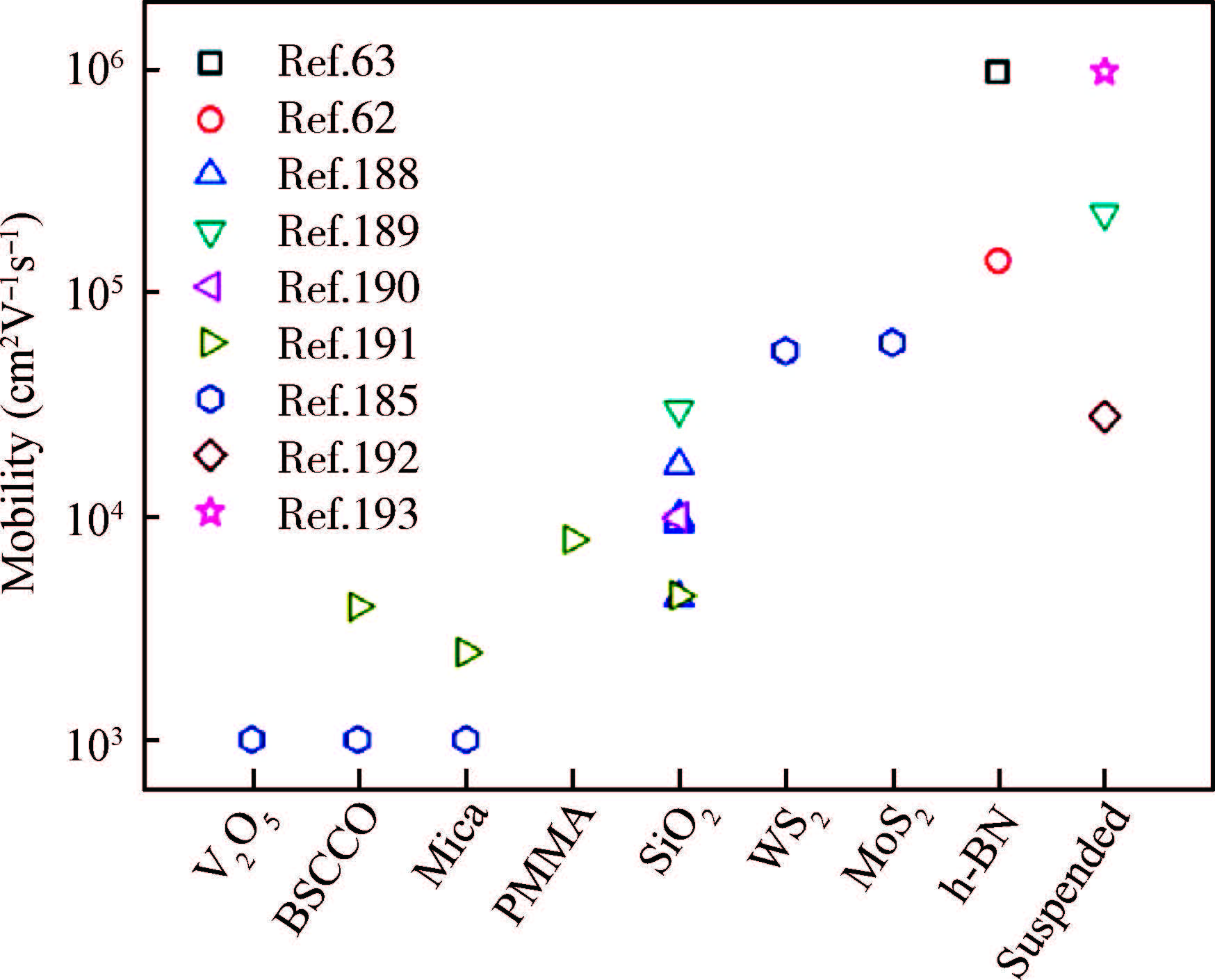
Fig. 1.  Carrier mobility of exfoliated monolayer graphene supported on several typical substrates at low temperatures (1.7-20 K) [5].

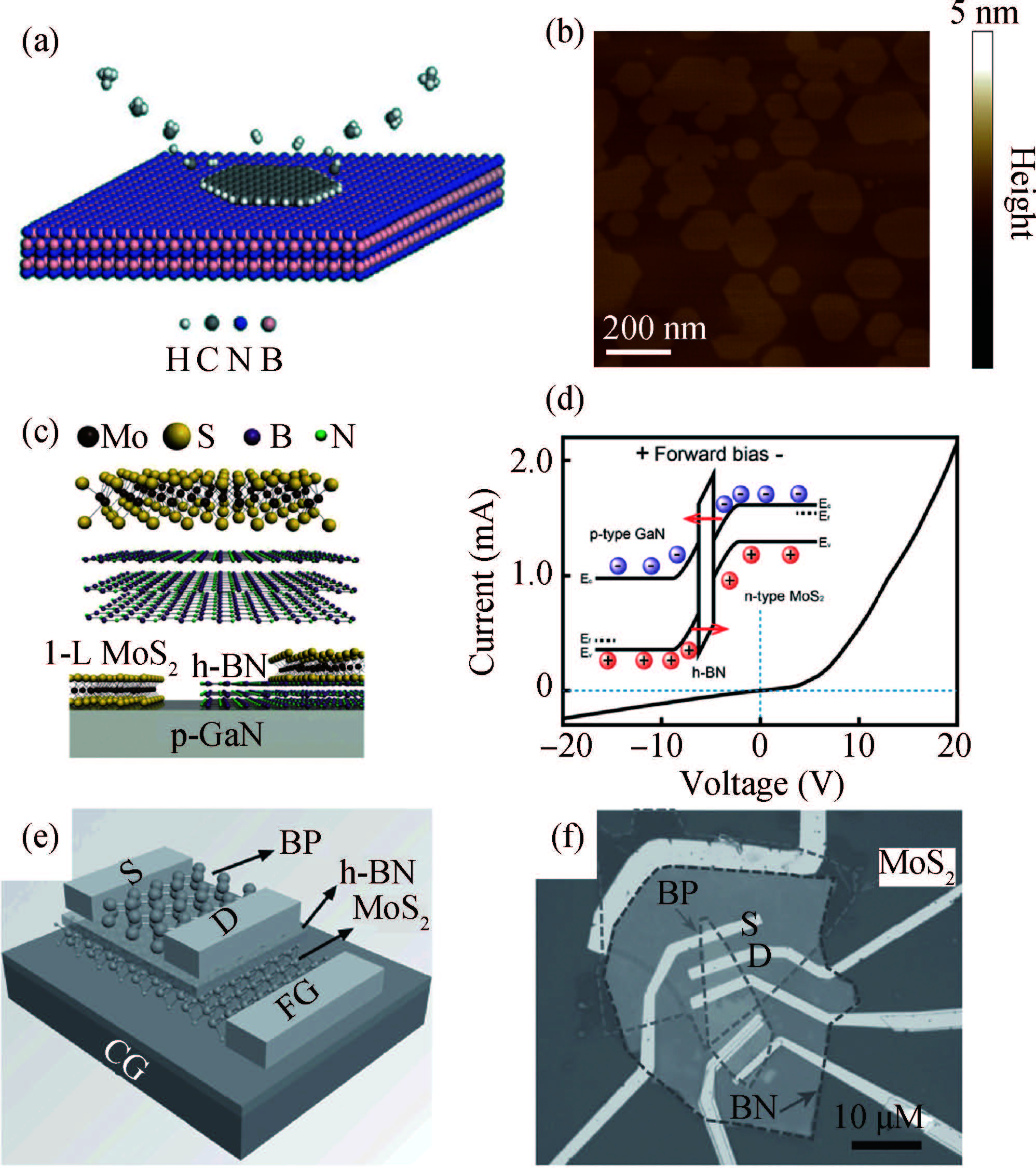
Fig. 2.  (Color online) (a) Schematic illustration of the epitaxial graphene growth on h-BN. (b) Zoomed-in AFM image of as-grown graphene domains on h-BN [13]. (c) Schematic of the MoS2/h-BN/p-GaN MIS heterojunction structure. (d) I-V curves for the MIS diode [22]. (e) Schematic of the BP/h-BN/MoS2 sandwich FGFET device structure. (f) Optical micrograph of a typical fabricated device. The dotted lines indicate the boundary of each material [23].

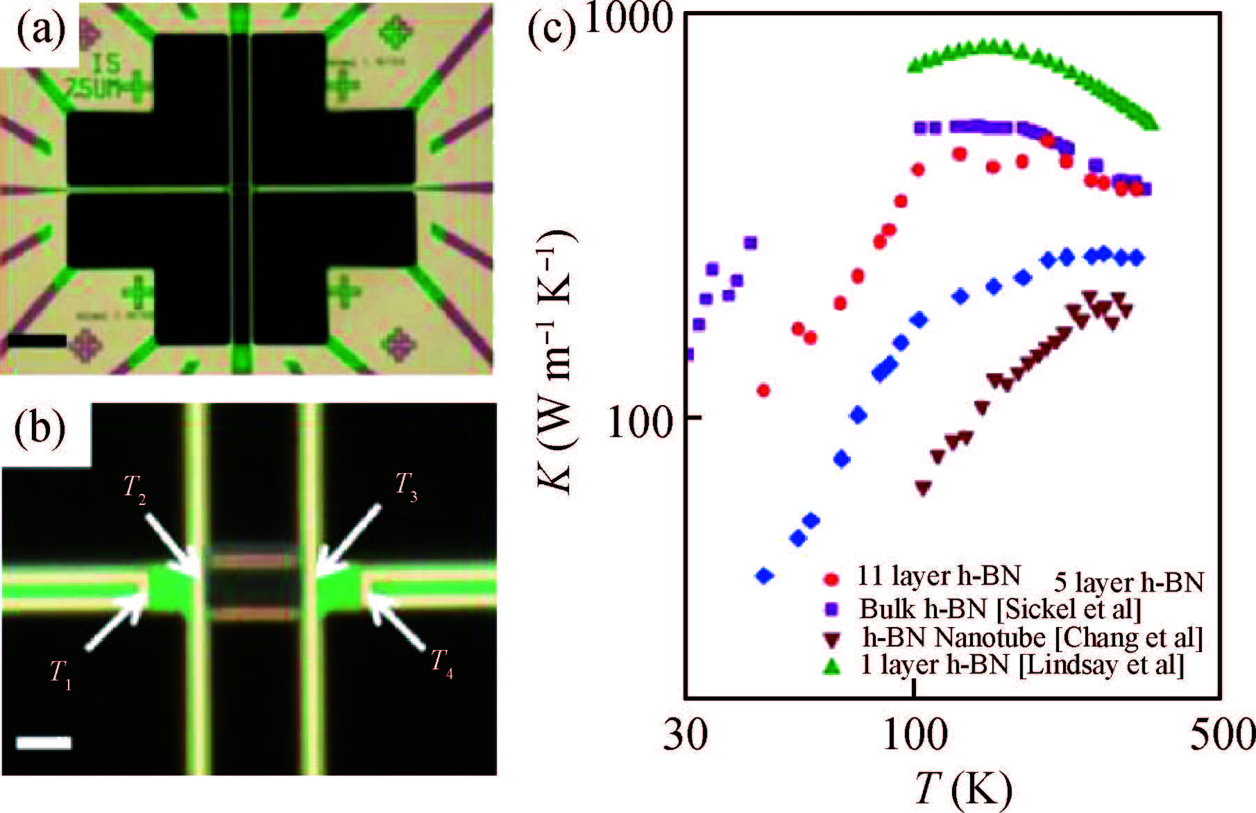
Fig. 3.  (Color online) Optical micrographs showing (a) the microbridge device and (b) an 11-layer h-BN sample suspended on the device used for thermal measurement. (c) Measured thermal conductance values of four h-BN samples [33].

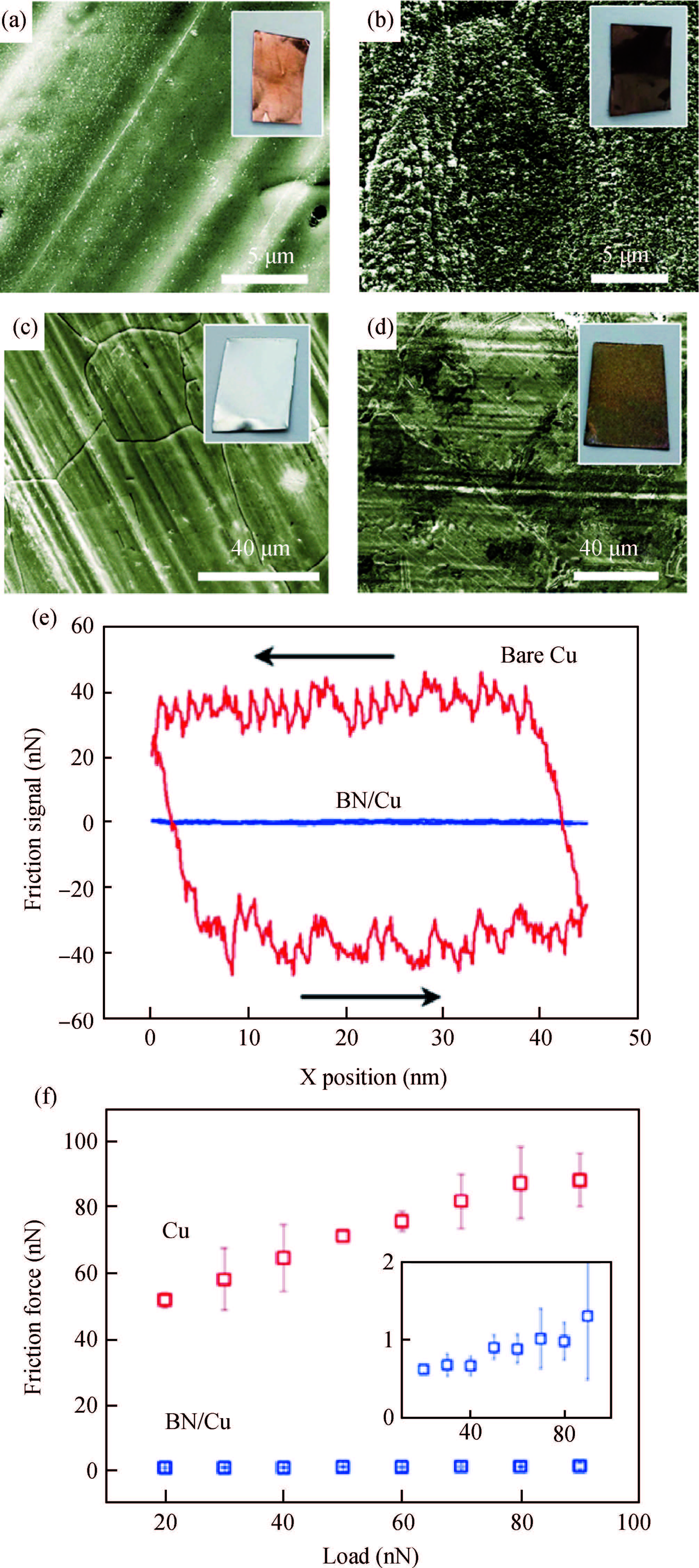
Fig. 4.  (Color online) h-BN thin films as high-performance oxidation-resistance coatings. (a, b) SEM images of Cu foils after oxidization with and without h-BN coatings at 500 ℃ for 30 min. (c, d) SEM images of stainless steel surface with and without h-BN coatings at up to 1100 ℃ for 30 min. With h-BN coating, both Cu and stainless steel can maintain their original color. Without h-BN coatings, their colors have changed because of oxidation [42]. (e) Friction force signal taken on the bare Cu surface and h-BN monolayer coating on Cu at an applied load of 40 nN. (f) The deduced friction force as a function of the applied load [43].

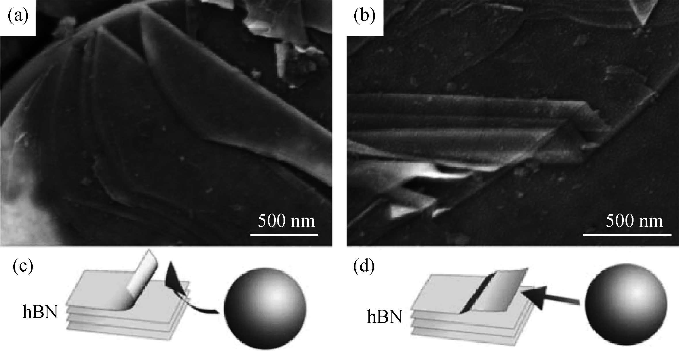
Fig. 5.  SEM images and corresponding diagrams illustrating two observed exfoliating mechanisms under the shear force created by milling balls: (a), (c) cleavage from the edge of an h-BN particle; (b), (d) thin sheets peeling off the top surface of an h-BN particle [53].

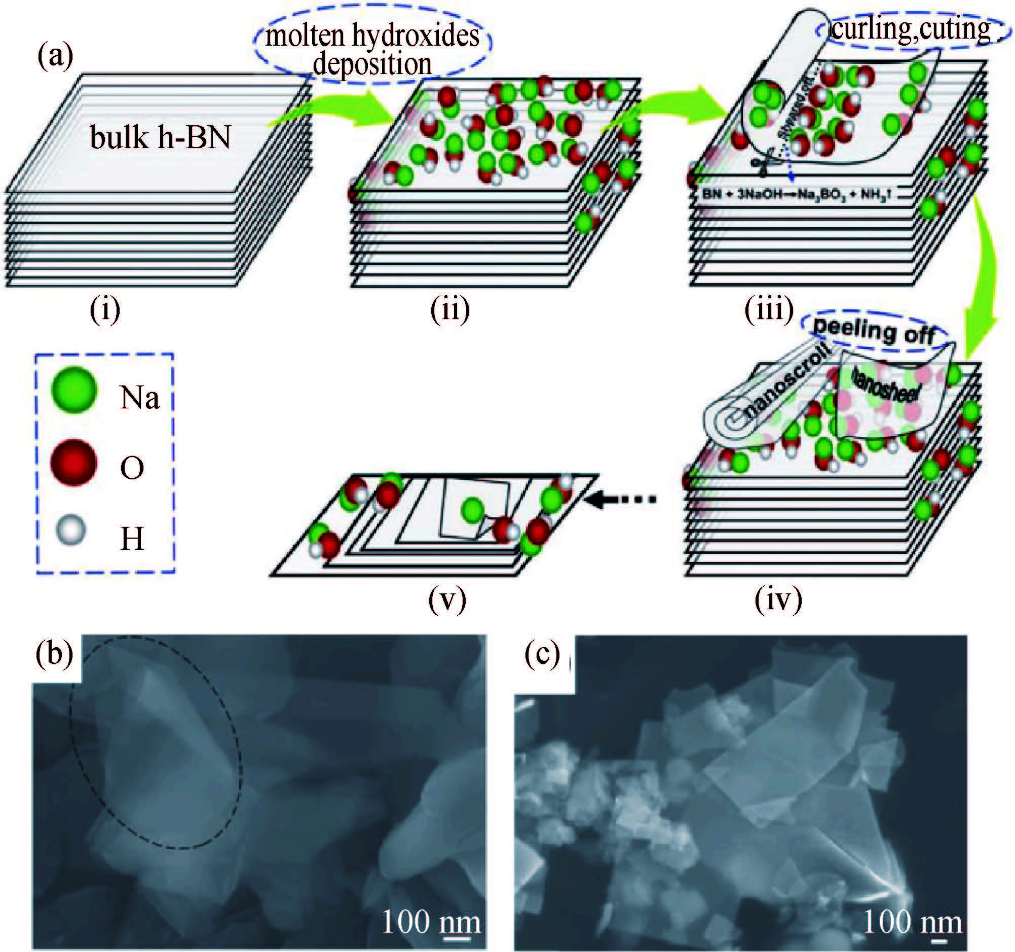
Fig. 6.  (Color online) (a) Illustration of the exfoliation mechanism. (b) Typical curved nanosheets several hundred nanometers in size (circled in black). (c) A very flat nanosheet [60].

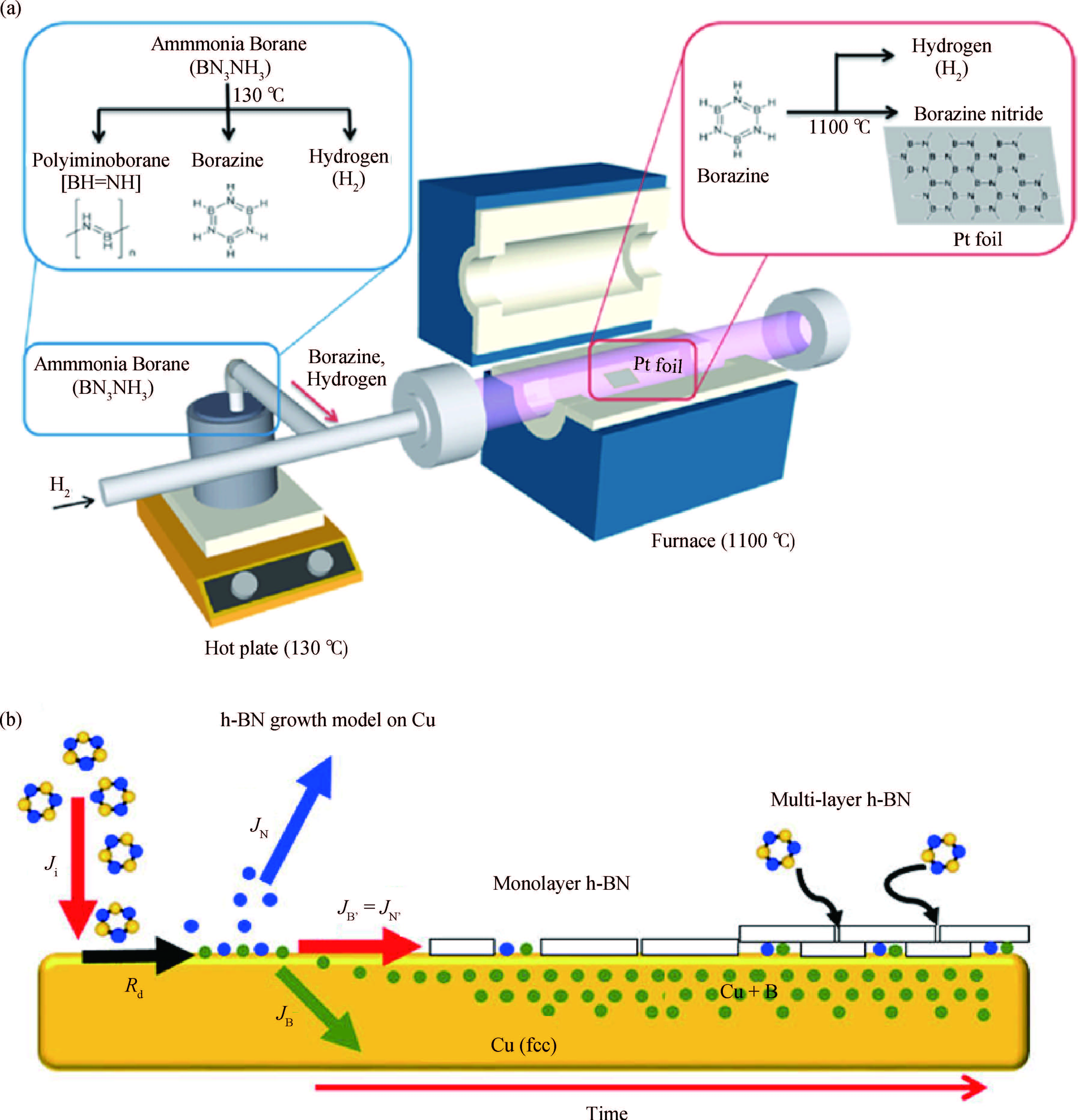
Fig. 7.  (Color online) Schematic diagrams of (a) the low pressure CVD system used for h-BN growth [69] and (b) h-BN growth mechanism on Cu propose by Kidambi et al. [70].

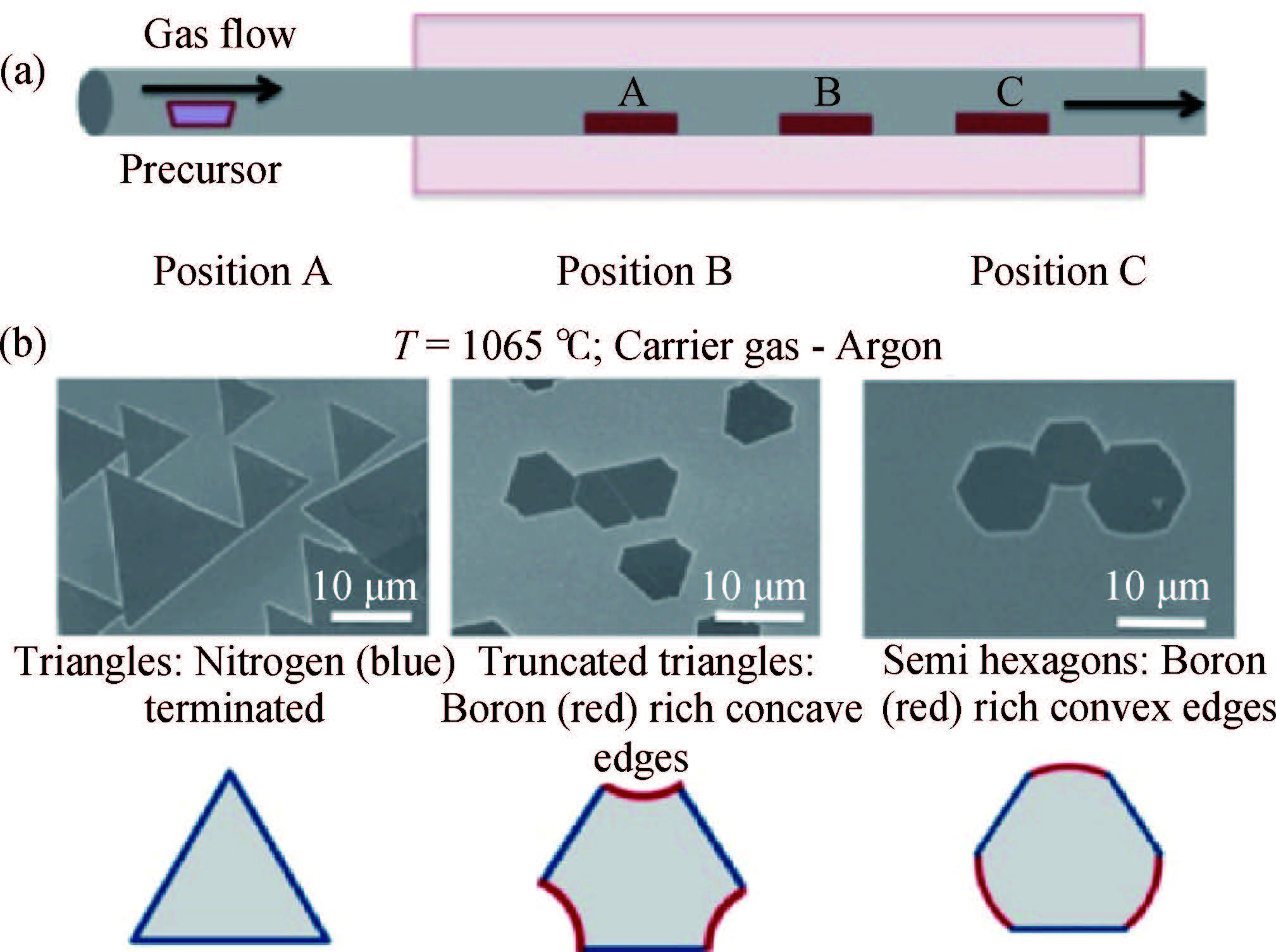
Fig. 8.  h-BN crystals grown at different conditions. (a) APCVD experimental setup for h-BN growth. (b) SEM images of the h-BN domains grown at 1065 ℃ using argon as a buffer gas [92].

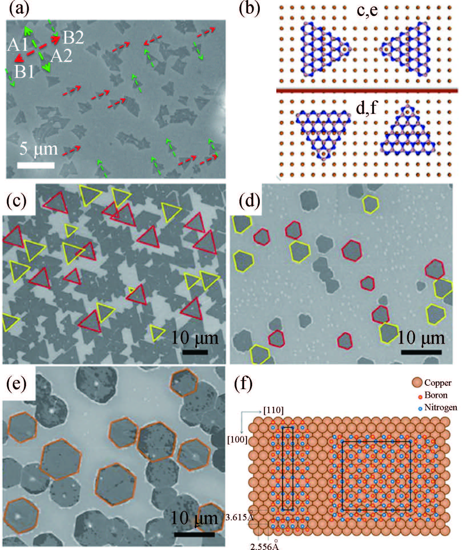
Fig. 9.  (Color online) (a) SEM images of BN islands on Cu foil and (b) real-space atomic model of four equivalent orientations of triangular BN crystallites on Cu(100) [95]. SEM images of the as-grown oriented (c) triangular, (d) asymmetric hexagonal and (e) hexagonal shaped h-BN domains, respectively. The red and yellow lines outline the h-BN domains which indicate 60° rotational difference from each other. (f) Schematic of the atomic arrangement of h-BN on Cu (110) with two different possible orientations [97].

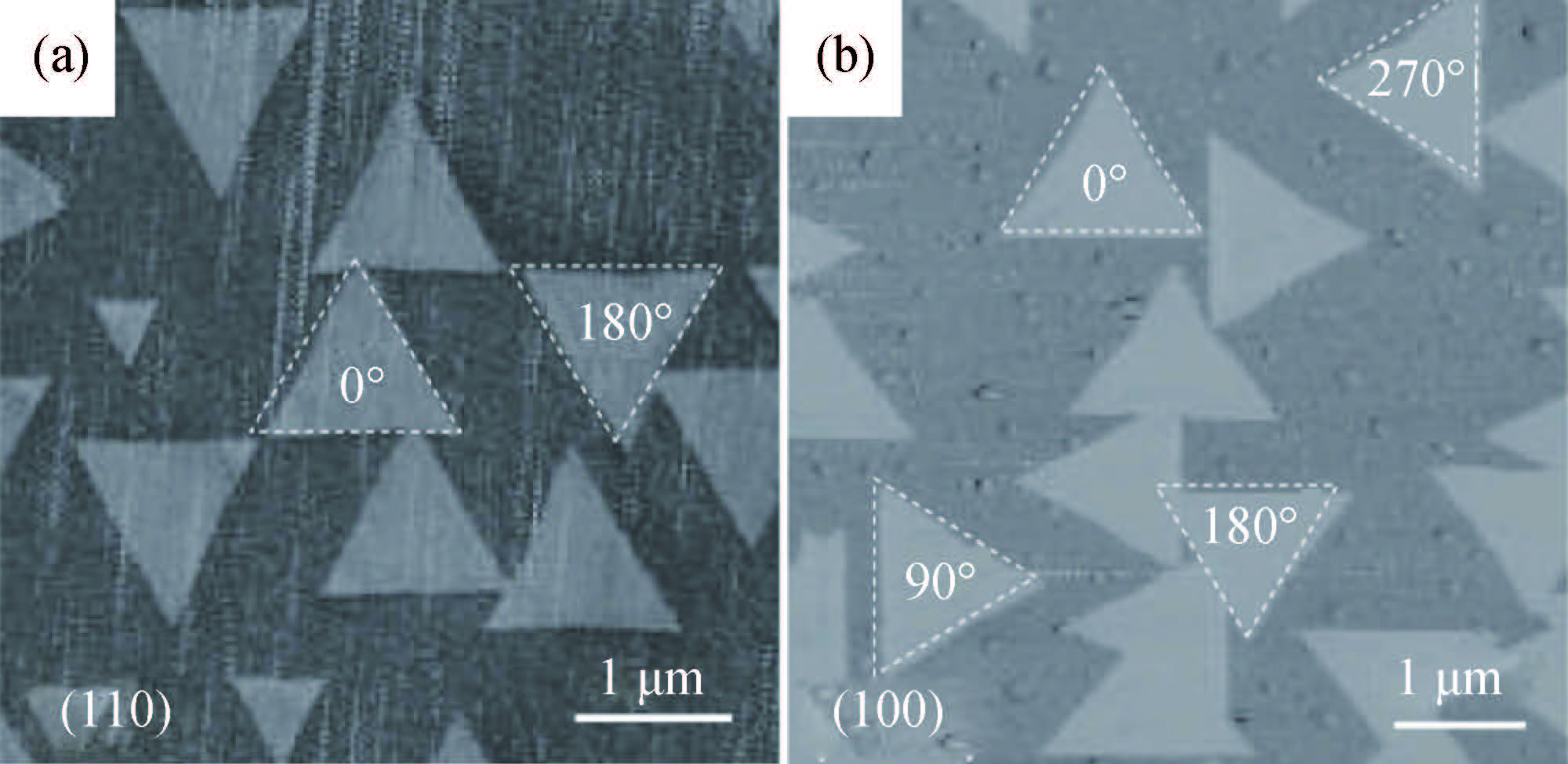
Fig. 10.  Epitaxial growth of 2D h-BN. Friction force images of h-BN domains grown on (a) Ge (110) and (b) Ge (100), respectively [98].

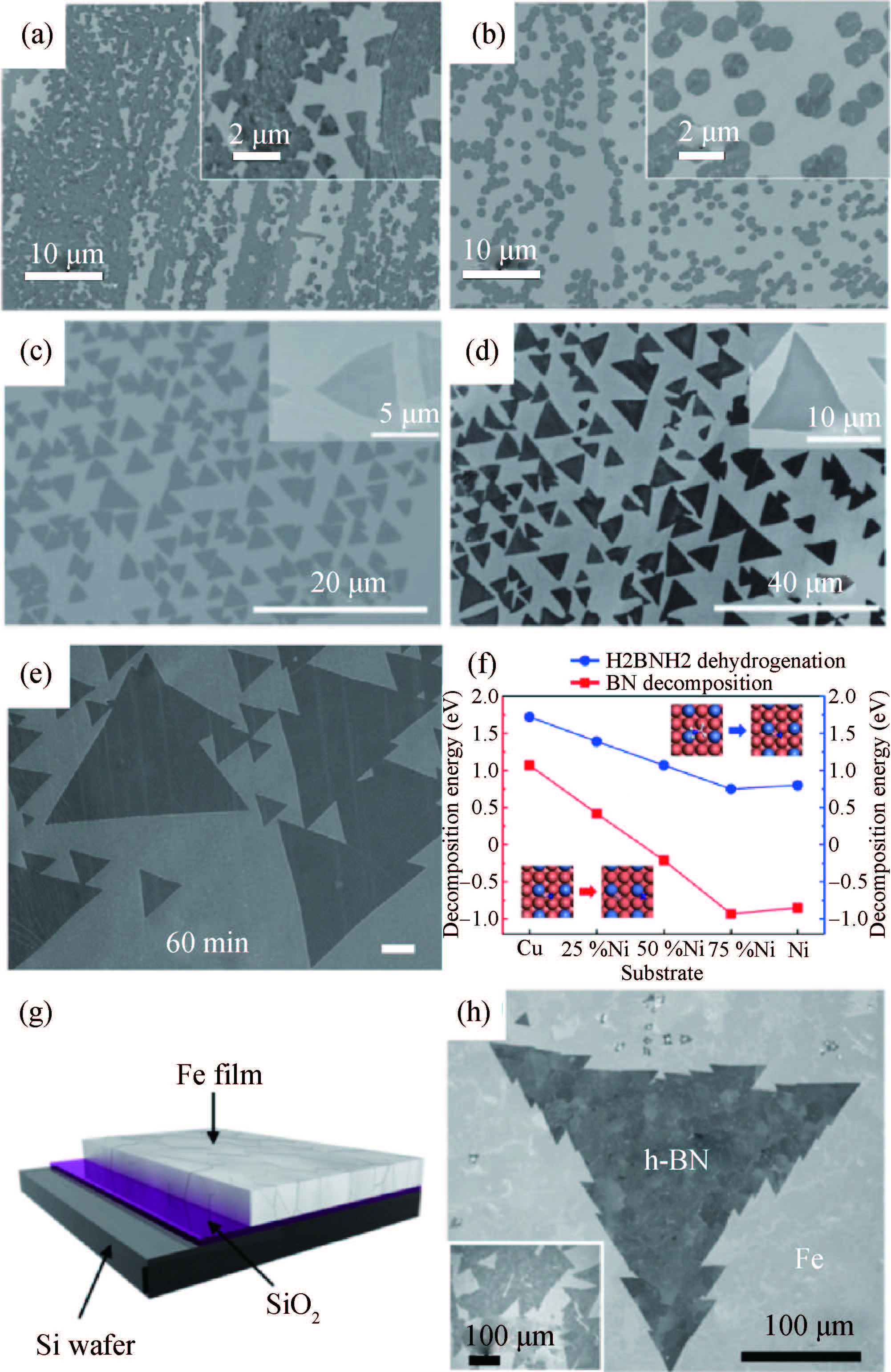
Fig. 11.  SEM images of (a) triangular and (b) hexagonal-shape h-BN domains grown on unpolished and polished Cu, respectively. The inset in each figure shows higher magnification [100]. SEM image of triangular-shaped h-BN domains (c) grown on Cu foil surface without pre-annealing (d) grown on annealed Cu surface for 6 h [101]. (e) Typical SEM images of h-BN grains grown on Cu-Ni alloy foils with 15 atom % Ni. (f) The molecular dynamic simulation of H2BNH2 dissociation on the surface of different substrates [102]. (g) Schematic of catalyst system composed of Fe/SiO2/Si. (h) SEM image of a large, tooth-edged h-BN domain grown on Fe(1000 nm)/SiO2(300 nm)/Si substrates. Inset: corresponding low magnification SEM image [103].

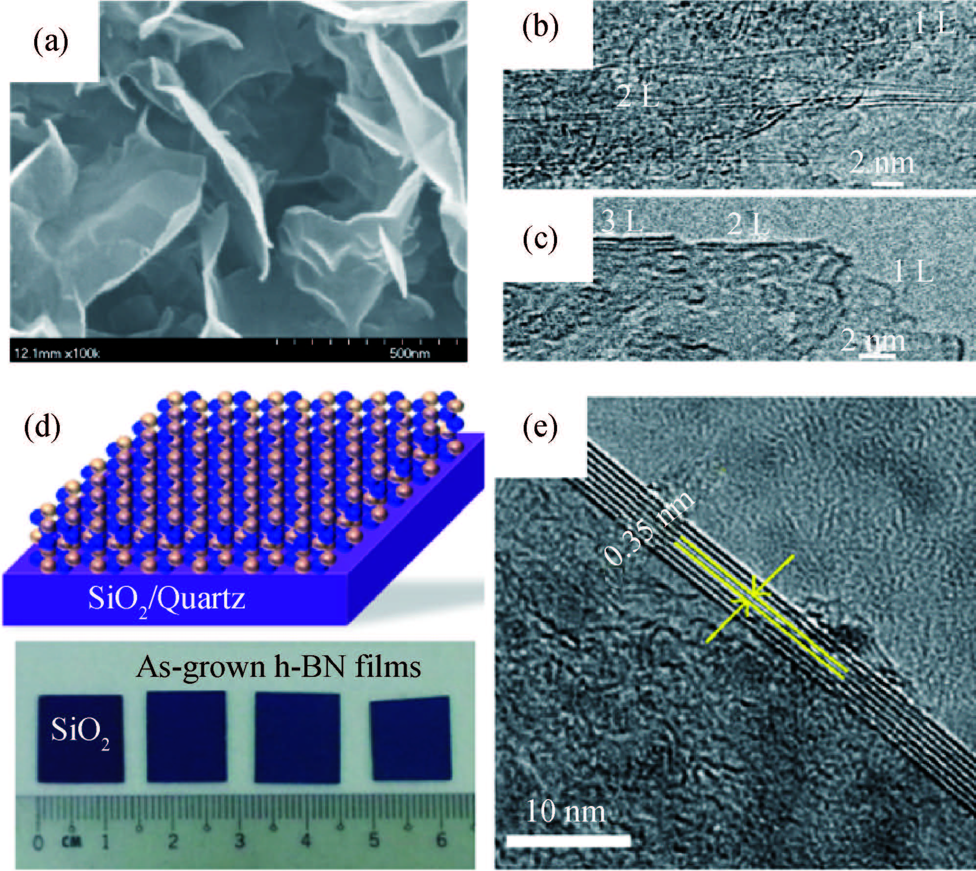
Fig. 12.  2D h-BN synthesized using catalysis-free approaches. (a) SEM images of the BN sheets grown on silicon substrates. High magnification TEM images showing the edges of the BN sheets consisting of 1-2 (b), 1-3 (c) atomic layers, respectively [105]. (d) Schematic diagram (top) and photograph (bottom) of direct grown NCBN films on SiO2/Si substrates. (e) Cross-section TEM image taken at a folded edge showing 7 NCBN layers [106].

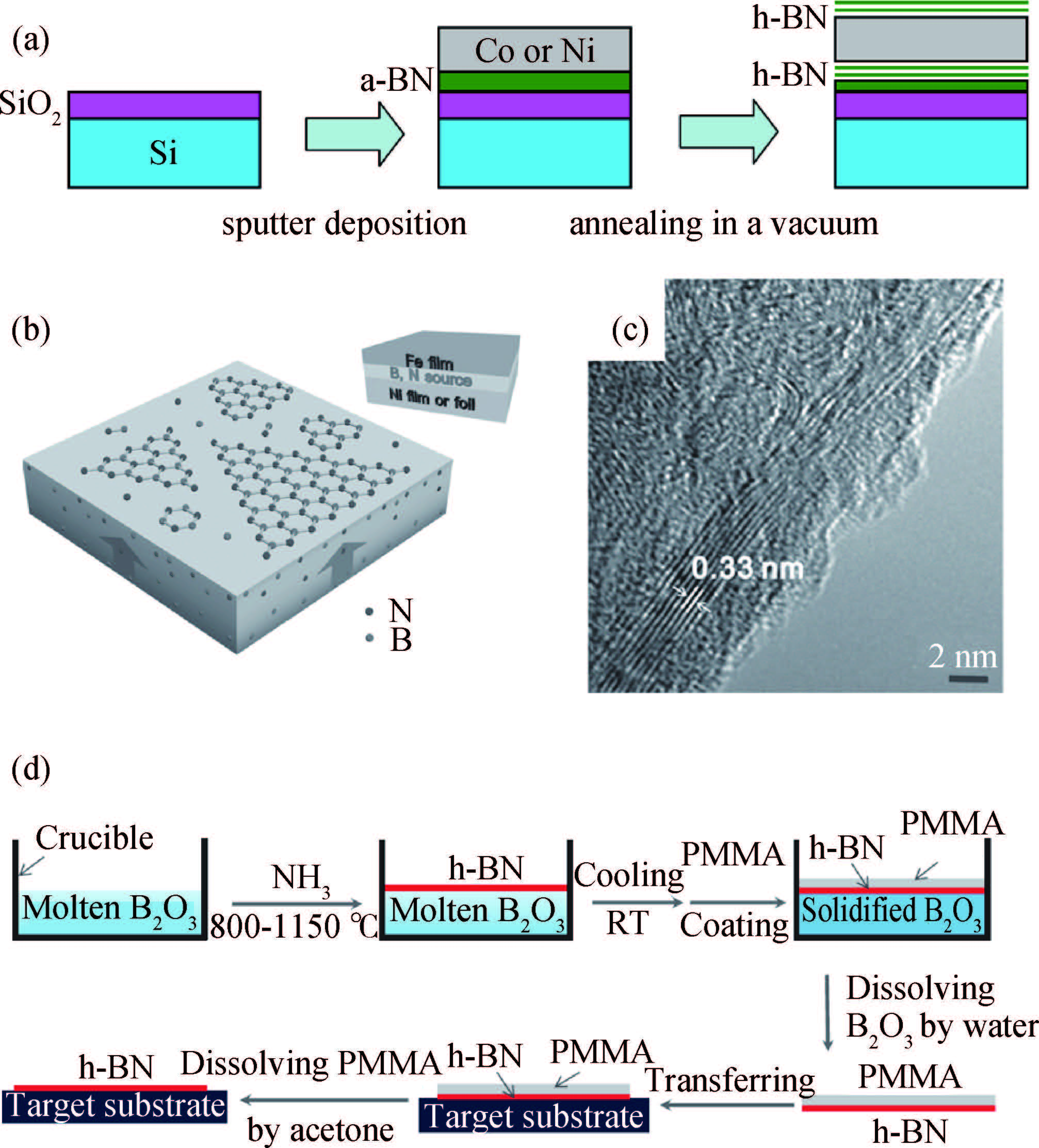
Fig. 13.  (a) Schematic of the growth method for a h-BN film by annealing a Co (Ni)/amorphous BN/SiO2 structure in vacuum [108]. (b) Schematic of h-BN synthesis by the vacuum annealing of sandwiched substrates Fe/(B, N)/Ni. (c) High resolution TEM image of a h-BN film edge [110]. (d) Schematic illustration of the self-limiting reaction process of molten B2O3 and gaseous NH3 for h-BN film synthesis and the transference of the h-BN film [112].

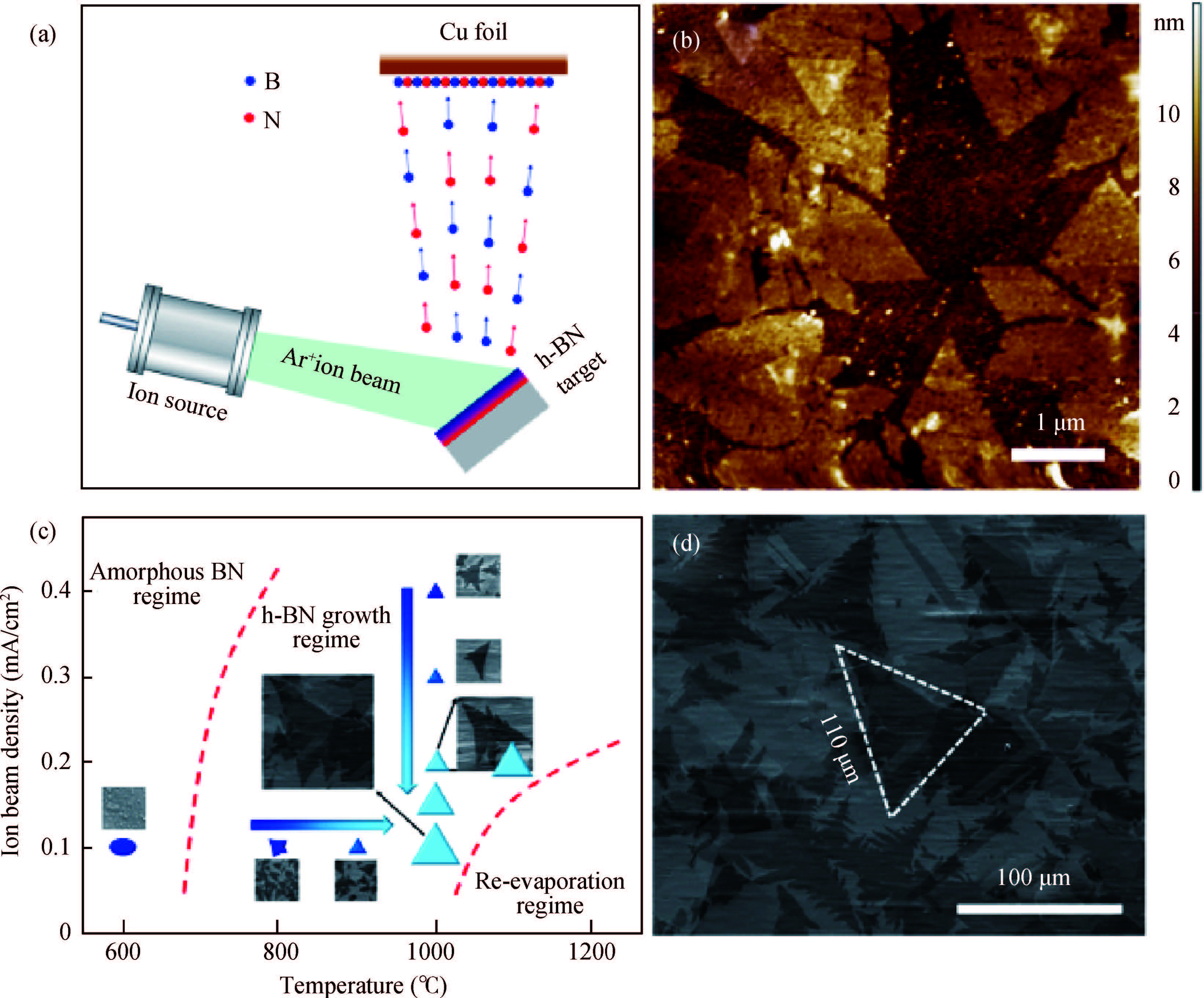
Fig. 14.  (Color online) Synthesis of 2D h-BN using IBSD. (a) Schematic diagram of the IBSD process. (b) AFM images of h-BN domains grown on Cu foils transferred onto a SiO2/Si substrate [113]. (c) Schematic drawing of the dependence of h-BN domain size on the ion beam density and the growth temperature, from which three regimes can be identified, as indicated by the red dashed lines. (d) SEM images of the h-BN domains prepared on the Ni foils [32].

[1]
Ferrari A C, Bonaccorso F, Fal'ko V, et al. Science and technology roadmap for graphene, related two-dimensional crystals, and hybrid systems. Nanoscale, 2015, 7(11):4598 doi: 10.1039/C4NR01600A
[2]
Geim A K, Novoselov K S. The rise of graphene. Nat Mater, 2007, 6(3):183 doi: 10.1038/nmat1849
[3]
Zhang H. Ultrathin two-dimensional nanomaterials. ACS Nano, 2015, 9(10):9451 doi: 10.1021/acsnano.5b05040
[4]
Bhimanapati G R, Lin Z, Meunier V. Recent advances in twodimensional materials beyond graphene. ACS Nano, 2015, 9(12):11509 doi: 10.1021/acsnano.5b05556
[5]
Yin J, Li J, Hang Y, et al. Boron nitride nanostructures:fabrication, functionalization and applications. Small, 2016, 12(22):2942 doi: 10.1002/smll.201600053
[6]
Golberg D, Bando Y, Huang Y, et al. Boron nitride nanotubes and nanosheets. ACS Nano, 2010, 4(6):2979 doi: 10.1021/nn1006495
[7]
Pakdel A, Bando Y, Golberg D. Nano boron nitride flatland. Chem Soc Rev, 2014, 43(3):934 doi: 10.1039/C3CS60260E
[8]
Kubota Y, Watanabe K, Tsuda O, et al. Deep ultraviolet lightemitting hexagonal boron nitride synthesized at atmospheric pressure. Science, 2007, 317(5840):932 doi: 10.1126/science.1144216
[9]
Lee K H, Shin H J, Lee J, et al. Large-scale synthesis of high-quality hexagonal boron nitride nanosheets for large-area graphene electronics. Nano Lett, 2012, 12(2):714 doi: 10.1021/nl203635v
[10]
Giovannetti G, Khomyakov P, Brocks G, et al. Substrate induced band gap in graphene on hexagonal boron nitride:ab initio density functional calculations. Phys Rev B, 2007, 76(7):073103 doi: 10.1103/PhysRevB.76.073103
[11]
Dean C R, Young A F, Meric I, et al. Boron nitride substrates for high-quality graphene electronics. Nat Nanotechnol, 2010, 5(10):722 doi: 10.1038/nnano.2010.172
[12]
Mayorov A S, Gorbachev R V, Morozov S V, et al, Micrometerscale ballistic transport in encapsulated graphene at room temperature. Nano Lett, 2011, 11(6):2396 doi: 10.1021/nl200758b
[13]
Yang W, Chen G R, Shi Z W, et al. Epitaxial growth of singledomain graphene on hexagonal boron nitride. Nat Mater, 2013, 12(9):792 doi: 10.1038/nmat3695
[14]
Gibb A L, Alem N, Chen J H, et al. Atomic resolution imaging of grain boundary defects in monolayer chemical vapor depositiongrown hexagonal boron nitride. J Am Chem Soc, 2013, 135(18):6758 doi: 10.1021/ja400637n
[15]
Cretu O, Lin Y C, Suenaga K. Evidence for active atomic defects in monolayer hexagonal boron nitride:a new mechanism of plasticity in two-dimensional materials. Nano Lett, 2014, 14(2):1064 doi: 10.1021/nl404735w
[16]
Bresnehan M S, Hollander M J, Wetherington M, et al. Integration of hexagonal boron nitride with quasi-freestanding epitaxial graphene:toward wafer-scale, high-performance devices. ACS Nano, 2012, 6(6):5234 doi: 10.1021/nn300996t
[17]
Britnell L, Gorbachev R V, Jalil R, et al. Field-effect tunneling transistor based on vertical graphene heterostructures. Science, 2012, 335(6071):947 doi: 10.1126/science.1218461
[18]
Wang J, Yao Q, Huang C W, et al. High mobility MoS2 transistor with low Schottky barrier contact by using atomic thick h-BN as a tunneling layer. Adv Mater, 2016, 28(37):8302 doi: 10.1002/adma.v28.37
[19]
Meng J H, Liu X, Zhang X W, et al. Interface engineering for highly efficient graphene-on-silicon Schottky junction solar cells by introducing a hexagonal boron nitride interlayer. Nano Energy, 2016, 28:44 doi: 10.1016/j.nanoen.2016.08.028
[20]
Cui X, Lee G H, Kim Y D, et al. Multi-terminal transport measurements of MoS2 using a van der Waals heterostructure device platform. Nat Nanotech, 2015, 10(6):534 doi: 10.1038/nnano.2015.70
[21]
Li L, Ye G J, Tran V, et al. Quantum oscillations in a twodimensional electron gas in black phosphorus thin films. Nat Nanotechnol, 2015, 10(7):608 doi: 10.1038/nnano.2015.91
[22]
Jeong H, Bang S, Oh H M, et al. Semiconductor-insulator- semiconductor diode consisting of monolayer MoS2, h-BN, and GaN heterostructure. ACS Nano, 2015, 9(10):10032 doi: 10.1021/acsnano.5b04233
[23]
Li D, Wang X, Zhang Q, et al. Nonvolatile floating-gate memories based on stacked black phosphorus-boron nitride-MoS2 heterostructures. Adv Funct Mater, 2015, 25(47):7360 doi: 10.1002/adfm.v25.47
[24]
Britnell L, Gorbachev R V, Jalil R, et al. Electron tunneling through ultrathin boron nitride crystalline barriers. Nano Lett, 2012, 12(3):1707 doi: 10.1021/nl3002205
[25]
Tang S, Wang H, Wang H S, et al. Silane-catalysed fast growth of large single-crystalline graphene on hexagonal boron nitride. Nat Commun, 2015, 6:6499 doi: 10.1038/ncomms7499
[26]
Levendorf M P, Kim C J, Brown L, et al. Graphene and boron nitride lateral heterostructures for atomically thin circuitry. Nature, 2012, 488(7413):627 doi: 10.1038/nature11408
[27]
Liu Z, Ma L L, Shi G, et al. In-plane heterostructures of graphene and hexagonal boron nitride with controlled domain sizes. Nat Nanotechnol, 2013, 8(2):119 doi: 10.1038/nnano.2012.256
[28]
Liu Z, Song L, Zhao S Z, et al. Direct growth of graphene/hexagonal boron nitride stacked layers. Nano Lett, 2011, 11(5):2032 doi: 10.1021/nl200464j
[29]
Wang M, Jang S K, Jang W J, et al. A platform for large-scale graphene electronics-CVD growth of single-layer graphene on CVD-grown hexagonal boron nitride. Adv Mater, 2013, 25(19):2746 doi: 10.1002/adma.v25.19
[30]
Meng J H, Zhang X W, Wang H L, et al. Synthesis of in-plane and stacked graphene/hexagonal boron nitride heterostructures by combining with ion beam sputtering deposition and chemical vapor deposition. Nanoscale, 2015, 7(38):16046 doi: 10.1039/C5NR04490A
[31]
Gorbachev R V, Riaz I, Nair R R, et al. Hunting for monolayer boron nitride:optical and Raman signatures. Small, 2011, 7:465 doi: 10.1002/smll.201001628
[32]
Wang H L, Zhang X W, Liu H, et al. Synthesis of large-sized single-crystal hexagonal boron nitride domains on nickel foils by ion beam sputtering deposition. Adv Mater, 2015, 27(48):8109 doi: 10.1002/adma.201504042
[33]
Jo I, Pettes M T, Kim J, et al. Thermal conductivity and phonon transport in suspended few-layer hexagonal boron nitride. Nano Lett, 2013, 13(2):550 doi: 10.1021/nl304060g
[34]
Lindsay L, Broido D A. Enhanced thermal conductivity and isotope effect in single-layer hexagonal boron nitride. Phys Rev B, 2012, 85(15):035436 https://www.researchgate.net/publication/235494934_Enhanced_thermal_conductivity_and_isotope_effect_in_single-layer_hexagonal_boron_nitride
[35]
Alam M T, Bresnehan M S, Robinson J A, et al. Thermal conductivity of ultra-thin chemical vapor deposited hexagonal boron nitride films. Appl Phys Lett, 2014, 104(1):013113 doi: 10.1063/1.4861468
[36]
Song W L, Wang P, Cao L, et al. Polymer/boron nitride nanocomposite materials for superior thermal transport performance. Angew Chem Int Ed, 2012, 51(26):6498 doi: 10.1002/anie.201201689
[37]
Taha-Tijerina J, Narayanan T N, Gao G H, et al. Electrically insulating thermal nano-oils using 2D fillers. ACS Nano, 2012, 6(2):1214 doi: 10.1021/nn203862p
[38]
Lee C, Wei X D, Kysar J W, et al. Measurement of the elastic properties and intrinsic strength of monolayer graphene. Science, 2008, 321(5887):385 doi: 10.1126/science.1157996
[39]
Bosak A, Serrano J, Krisch M, et al. Elasticity of hexagonal boron nitride:inelastic X-ray scattering measurements. Phys Rev B, 2006, 73(4):041402(R)
[40]
Wang Y, Shi Z, Yin J. Boron nitride nanosheets:large-scale exfoliation in methanesulfonic acid and their composites with polybenzimidazole. J Mater Chem, 2011, 21(30):11371 doi: 10.1039/c1jm10342c
[41]
Jin X, Fu N, Ding H, et al. Effects of h-BN on the thermal and mechanical properties of PBT/PC/ABS blend based composites. RSC Adv, 2015, 5(72):58171 doi: 10.1039/C5RA09746K
[42]
Liu Z, Gong Y, Zhou W, et al. Ultrathin high-temperature oxidation-resistant coatings of hexagonal boron nitride. Nat Commun, 2013, 4:2541 https://www.researchgate.net/publication/261796059_Ultrathin_high-temperature_oxidation-resistant_coatings_of_hexagonal_boron_nitride
[43]
Li X, Yin J, Zhou J, et al. Large area hexagonal boron nitride monolayer as efficient atomically thick insulating coating against friction and oxidation. Nanotechnology, 2014, 25(10):105701 doi: 10.1088/0957-4484/25/10/105701
[44]
Qi J, Qian X, Qi L, et al. Strain-engineering of band gaps in piezoelectric boron nitride nanoribbons. Nano Lett, 2012, 12(3):1224 doi: 10.1021/nl2035749
[45]
Duerloo K A N, Reed E J. Flexural electromechanical coupling:a nanoscale emergent property of boron nitride bilayers. Nano Lett, 2013, 13(4):1681 doi: 10.1021/nl4001635
[46]
Gao M, Lyalin A, Taketsugu T. Catalytic activity of Au and Au2 on the h-BN surface:adsorption and activation of O2. J Phys Chem C, 2012, 116(16):9054 doi: 10.1021/jp300684v
[47]
Lin Y, Bunker C E, Fernando K A S, et al. Aqueously dispersed silver nanoparticle-decorated boron nitride nanosheets for reusable, thermal oxidation-resistant surface enhanced Raman spectroscopy (SERS) devices. ACS Appl Mater Interfaces, 2012, 4(2):1110 doi: 10.1021/am201747d
[48]
Novoselov K S, Geim A K, Morozov S V, et al. Electric field effect in atomically thin carbon films. Science, 2004, 306(5696):666 doi: 10.1126/science.1102896
[49]
Novoselov K S, Jiang D, Schedin F, et al. Two-dimensional atomic crystals. Proc Nat Acad Sci USA, 2005, 102(30):10451 doi: 10.1073/pnas.0502848102
[50]
Pacile D, Meyer J C, Girit C O, et al. The two-dimensional phase of boron nitride:few-atomic-layer sheets and suspended membranes. Appl Phys Lett, 2008, 92(13):133107 doi: 10.1063/1.2903702
[51]
Pakdel A, Zhi C Y, Bando Y. Low-dimensional boron nitride nanomaterials. Mater Today, 2012, 15(6):256 doi: 10.1016/S1369-7021(12)70116-5
[52]
Xu M S, Liang T, Shi M M, et al. Graphene-like two-dimensional materials. Chem Rev, 2013, 113(5):3766 doi: 10.1021/cr300263a
[53]
Li L H, Chen Y, Behan G, et al. Large-scale mechanical peeling of boron nitride nanosheets by low-energy ball milling. J Mater Chem, 2011, 21(32):11862 doi: 10.1039/c1jm11192b
[54]
Han W Q, Wu L, Zhu Y, et al. Structure of chemically derived mono- and few-atomic-layer boron nitride sheets. Appl Phys Lett, 2008, 93(22):223103 doi: 10.1063/1.3041639
[55]
Coleman J N, Lotya M, O'Neill A, et al. Two-dimensional nanosheets produced by liquid exfoliation of layered materials. Science, 2011, 331(6017):568 doi: 10.1126/science.1194975
[56]
Smith R J, King P J, Lotya M, et al. Large-scale exfoliation of inorganic layered compounds in aqueous surfactant solutions. Adv Mater, 2011, 23(24):3944 https://www.researchgate.net/profile/Andrew_Minett/publication/51528178_Large-Scale_Exfoliation_of_Inorganic_Layered_Compounds_in_Aqueous_Surfactant_Solutions/links/02e7e5193182d696ce000000.pdf
[57]
Zhi C Y, Bando Y, Tang C C, et al. Large-scale fabrication of few-atomic-layer boron nitride nanosheets and their utilization in polymeric composites with improved thermal and mechanical properties. Adv Mater, 2009, 21(28):288
[58]
Warner J H, Rummeli M H, Bachmatiuk A, et al. Atomic resolution imaging and topography of boron nitride sheets produced by chemical exfoliation. ACS Nano, 2010, 4(3):1299 doi: 10.1021/nn901648q
[59]
Lin Y, Williams T V, Connell J W. Soluble, exfoliated hexagonal boron nitride nanosheets. J Phys Chem Lett, 2010, 1(1):277 doi: 10.1021/jz9002108
[60]
Li X L, Hao X P, Zhao M W, et al. Exfoliation of hexagonal boron nitride by molten hydroxides. Adv Mater, 2013, 25(15):2200 doi: 10.1002/adma.201204031
[61]
Bao J, Jeppson K, Edwards M, et al. Synthesis and applications of two-dimensional hexagonal boron nitride in electronics manufacturing. Electron Mater Lett, 2016, 12(1):1 doi: 10.1007/s13391-015-5308-2
[62]
Paffett M T, Simonson R J, Papin P, et al. Borazine adsorption and decomposition at Pt(111) and Ru(001) surfaces. Surf Sci, 1990, 232(3):286 doi: 10.1016/0039-6028(90)90121-N
[63]
Nagashima A, Tejima N, Gamou Y, et al. Electronic structure of monolayer hexagonal boron nitride physisorbed on metal surfaces. Phys Rev Lett, 1995, 75(21):3918 doi: 10.1103/PhysRevLett.75.3918
[64]
Corso M, Auwarter W, Muntwiler M, et al. Boron nitride nanomesh. Science, 2004, 303(5655):217 doi: 10.1126/science.1091979
[65]
Auwarter W, Kreutz T J, Greber T, et al. XPD and STM investigation of hexagonal boron nitride on Ni(111). Surf Sci, 1999, 429(1-3):229 doi: 10.1016/S0039-6028(99)00381-7
[66]
Shi Y, Hamsen C, Jia X, et al. Synthesis of few-layer hexagonal boron nitride thin film by chemical vapor deposition. Nano Lett, 2010, 10(10):4134 doi: 10.1021/nl1023707
[67]
Song L, Ci L, Lu H, et al. Large scale growth and characterization of atomic hexagonal boron nitride layers. Nano Lett, 2010, 10(8):3209 doi: 10.1021/nl1022139
[68]
Kim K K, Hsu A, Jia X, et al. Synthesis of monolayer hexagonal boron nitride on Cu foil using chemical vapor deposition. Nano Lett, 2012, 12(1):161 doi: 10.1021/nl203249a
[69]
Kim G, Jang A R, Jeong H Y, et al. Growth of high-crystalline, single-layer hexagonal boron nitride on recyclable platinum foil. Nano Lett, 2013, 13(4):1834 doi: 10.1021/nl400559s
[70]
Kidambi P R, Blume R, Kling J, et al. In situ observations during chemical vapor deposition of hexagonal boron nitride on polycrystalline copper. Chem Mater, 2014, 26(22):6380 doi: 10.1021/cm502603n
[71]
Pierson H O. Boron nitride composites by chemical vapor deposition. J Compos Mater, 1975, 9(3):228 doi: 10.1177/002199837500900302
[72]
Rozenberg A S, Sinenko Y A, Chukanov N V. Regularities of pyrolytic boron nitride coating formation on a graphite matrix. J Mater Sci, 1993, 28(20):5528 doi: 10.1007/BF00367825
[73]
Middleman S. The role of gas-phase reactions in boron nitride growth by chemical vapor deposition. Mater Sci Eng A, 1993, 163(1):135 doi: 10.1016/0921-5093(93)90587-5
[74]
Chatterjee S, Luo Z, Acerce M, et al. Chemical vapor deposition of boron nitride nanosheets on metallic substrates via decaborane/ammonia reactions. Chem Mater, 2011, 23(20):4414 doi: 10.1021/cm201955v
[75]
Adams A C. Characterization of films formed by pyrolysis of borazine. J Electrochem Soc, 1981, 128(6):1378 doi: 10.1149/1.2127639
[76]
Auwarter W, Suter H U, Sachdev H, et al. Synthesis of one monolayer of hexagonal boron nitride on Ni(111) from BTrichloroborazine (ClBNH)3. Chem Mater, 2004, 16(2):343 doi: 10.1021/cm034805s
[77]
Muller F, Stowe K, Sachdev H. Symmetry versus commensurability:epitaxial growth of hexagonal boron nitride on Pt(111) from B-trichloroborazine (ClBNH)3. Chem Mater, 2005, 17(13):3464 doi: 10.1021/cm048629e
[78]
Constant G, Feurer R. Preparation and characterization of thin protective films in silica tubes by thermal decomposition of hexachloroborazine. J Less-Common Met, 1981, 82(1/2):113
[79]
Wolf G, Baumann J, Baitalow F, et al. Calorimetric process monitoring of thermal decomposition of B-N-H compounds. Thermochim Acta, 2000, 343(1/2):19 https://www.researchgate.net/publication/223433830_Calorimetric_Process_Monitoring_of_Thermal_Decomposition_of_B-N-H_Compounds
[80]
Kim K K, Hsu A, Jia X, et al. Synthesis and characterization of hexagonal boron nitride film as a dielectric layer for graphene devices. ACS Nano, 2012, 6(10):8583 doi: 10.1021/nn301675f
[81]
Han J, Lee J Y, Kwon H, et al. Synthesis of wafer-scale hexagonal boron nitride monolayers free of aminoborane nanoparticles by chemical vapor deposition. Nanotechnology, 2014, 25(14):145604 doi: 10.1088/0957-4484/25/14/145604
[82]
Tay R Y, Wang X, Tsang S H, et al. A systematic study of the atmospheric pressure growth of large-area hexagonal crystalline boron nitride film. J Mater Chem C, 2014, 2(9):1650 doi: 10.1039/c3tc32011a
[83]
Park J H, Park J C, Yun S J, et al. Large-area monolayer hexagonal boron nitride on Pt foil. ACS Nano, 2014, 8(8):8520 doi: 10.1021/nn503140y
[84]
Orofeo C M, Suzuki S, Kageshima H, et al. Growth and low-energy electron microscopy characterization of monolayer hexagonal boron nitride on epitaxial cobalt. Nano Res, 2013, 6(5):335 doi: 10.1007/s12274-013-0310-1
[85]
Koepke J C, Wood J D, Chen Y, et al. Role of pressure in the growth of hexagonal boron nitride thin films from ammoniaborane. Chem Mater, 2016, 28(12):4169 doi: 10.1021/acs.chemmater.6b00396
[86]
Wu Q, Park J H, Park S, et al. Single crystalline film of hexagonal boron nitride atomic monolayer by controlling nucleation seeds and domains. Sci Rep, 2015, 5:16159 doi: 10.1038/srep16159
[87]
Gao Y, Ren W, Ma T, et al. Repeated and controlled growth of monolayer, bilayer and few-layer hexagonal boron nitride on Pt foils. ACS Nano, 2013, 7(6):5199 doi: 10.1021/nn4009356
[88]
Kim S M, Hsu A, Park M H, et al. Synthesis of large-area multilayer hexagonal boron nitride for high material performance. Nat Commun, 2015, 6:8662 doi: 10.1038/ncomms9662
[89]
Fu L, Sun Y, Wu N, et al. Direct growth of MoS2/h-BN heterostructures via a sulfide-resistant alloy. ACS Nano, 2016, 10(2):2063 doi: 10.1021/acsnano.5b06254
[90]
Lee Y H, Liu K K, Lu A Y, et al. Growth selectivity of hexagonalboron nitride layers on Ni with various crystal orientations. RSC Adv, 2012, 2(1):111 doi: 10.1039/C1RA00703C
[91]
Khan M H, Huang Z, Xiao F, et al. Synthesis of large and few atomic layers of hexagonal boron nitride on melted copper. Sci Rep, 2015, 5:7743 doi: 10.1038/srep07743
[92]
Stehle Y, Meyer Ⅲ H M, Unocic R R, et al. Synthesis of hexagonal boron nitride monolayer:control of nucleation and crystal morphology. Chem Mater, 2015, 27(23):8041 doi: 10.1021/acs.chemmater.5b03607
[93]
Liu Y, Bhowmick S, Yakobson B I. BN white graphene with "colorful" edges:the energies and morphology. Nano Lett, 2011, 11(8):3113 doi: 10.1021/nl2011142
[94]
Zhang Z, Liu Y, Yang Y, et al. Growth mechanism and morphology of hexagonal boron nitride. Nano Lett, 2016, 16(2):1398 doi: 10.1021/acs.nanolett.5b04874
[95]
Liu L, Siegelb D A, Chen W, et al. Unusual role of epilayersubstrate interactions in determining orientational relations in van der Waals epitaxy. Proc Natl Acad Sci USA, 2014, 111(47):16670 doi: 10.1073/pnas.1405613111
[96]
Song X, Gao J, Nie Y, et al. Chemical vapor deposition growth of large-scale hexagonal boron nitride with controllable orientation. Nano Res, 2015, 8(10):3164 doi: 10.1007/s12274-015-0816-9
[97]
Tay R Y, Park H J, Ryu G H, et al. Synthesis of aligned symmetrical multifaceted monolayer hexagonal boron nitride single crystals on resolidified copper. Nanoscale, 2016, 8(4):2434 doi: 10.1039/C5NR08036C
[98]
Yin J, Liu X, Lu W, et al. Aligned growth of hexagonal boron nitride monolayer on germanium. Small, 2015, 11(40):5375 doi: 10.1002/smll.v11.40
[99]
Li J D, Li Y, Yin J, et al. Growth of polar hexagonal boron nitride monolayer on nonpolar copper with unique orientation. Small, 2016, 12(27):3645 doi: 10.1002/smll.v12.27
[100]
Tay R Y, Griep M H, Mallick G, et al, Growth of large singlecrystalline two-dimensional boron nitride hexagons on electropolished copper. Nano Lett, 2014, 14(2):839 doi: 10.1021/nl404207f
[101]
Wang L, Wu B, Chen J, et al. Monolayer hexagonal boron nitride films with large domain size and clean interface for enhancing the mobility of graphene-based field-effect transistors. Adv Mater, 2014, 26(10):1559 doi: 10.1002/adma.201304937
[102]
Lu G, Wu T, Yuan Q, et al. Synthesis of large single-crystal hexagonal boron nitride grains on Cu-Ni alloy. Nat Commun, 2015, 6:6160 doi: 10.1038/ncomms7160
[103]
Caneva S, Weatherup R S, Bayer B C, et al. Nucleation control for large, single crystalline domains of monolayer hexagonal boron nitride via Si-doped Fe catalysts. Nano Lett, 2015, 15(3):1867 doi: 10.1021/nl5046632
[104]
Yu J, Qin L, Hao Y, et al. Vertically aligned boron nitride nanosheets:chemical vapor synthesis, ultraviolet light emission and superhydrophobicity. ACS Nano, 2010, 4(1):414 doi: 10.1021/nn901204c
[105]
Qin L, Yu J, Li M, et al. Catalyst-free growth of mono- and fewatomic-layer boron nitride sheets by chemical vapor deposition. Nanotechnology, 2011, 22(21):215602 doi: 10.1088/0957-4484/22/21/215602
[106]
Tay R Y, Tsang S H, Loeblein M, et al. Direct growth of nanocrystalline hexagonal boron nitride films on dielectric substrates. Appl Phys Lett, 2015, 106(10):101901 doi: 10.1063/1.4914474
[107]
Jang A R, Hong S, Hyun C, et al. Wafer-scale and wrinkle-free epitaxial growth of single-orientated multilayer hexagonal boron nitride on sapphire. Nano Lett, 2016, 16(5):3360 doi: 10.1021/acs.nanolett.6b01051
[108]
Suzuki S, Pallares R M, Hibino H. Growth of atomically thin hexagonal boron nitride films by diffusion through a metal film and precipitation. J Phys D, 2012, 45:385304 doi: 10.1088/0022-3727/45/38/385304
[109]
Suzuki S, Pallares R M, Orofeo C M, et al. Boron nitride growth on metal foil using solid sources. J Vac Sci Technol B, 2013, 31(4):041804 doi: 10.1116/1.4810965
[110]
Zhang C, Fu L, Zhao S, et al. Controllable co-segregation synthesis of wafer-scale hexagonal boron nitride thin films. Adv Mater, 2014, 26(11):1776 doi: 10.1002/adma.201304301
[111]
Nakhaie S, Wofford J M, Schumann T, et al. Synthesis of atomically thin hexagonal boron nitride films on nickel foils by molecular beam epitaxy. Appl Phys Lett, 2015, 106(21):213108 doi: 10.1063/1.4921921
[112]
Yang X, Guan Z, Zeng M, et al. Facile synthesis of large-area ultrathin hexagonal BN films via self-limiting growth at the molten B2O3 surface. Small, 2013, 9(8):1353 doi: 10.1002/smll.201203126
[113]
Wang H L, Zhang X W, Meng J H, et al. Controlled growth of few-layer hexagonal boron nitride on copper foils using ion beam sputtering deposition. Small, 2015, 11(13):1542 doi: 10.1002/smll.v11.13
[114]
Sutter P, Lahiri J, Zahl P, et al. Scalable synthesis of uniform fewlayer hexagonal boron nitride dielectric films. Nano Lett, 2013, 13(1):276 doi: 10.1021/nl304080y
  • Search

    Advanced Search >>

    GET CITATION

    shu

    Export: BibTex EndNote

    Article Metrics

    Article views: 7794 Times PDF downloads: 195 Times Cited by: 0 Times

    History

    Received: 28 October 2016 Revised: 25 November 2016 Online: Published: 01 March 2017

    Catalog

      Email This Article

      User name:
      Email:*请输入正确邮箱
      Code:*验证码错误
      Haolin Wang, Yajuan Zhao, Yong Xie, Xiaohua Ma, Xingwang Zhang. Recent progress in synthesis of two-dimensional hexagonal boron nitride[J]. Journal of Semiconductors, 2017, 38(3): 031003. doi: 10.1088/1674-4926/38/3/031003 ****H L Wang, Y J Zhao, Y Xie, X H Ma, X W Zhang. Recent progress in synthesis of two-dimensional hexagonal boron nitride[J]. J. Semicond., 2017, 38(3): 031003. doi: 10.1088/1674-4926/38/3/031003.
      Citation:
      Haolin Wang, Yajuan Zhao, Yong Xie, Xiaohua Ma, Xingwang Zhang. Recent progress in synthesis of two-dimensional hexagonal boron nitride[J]. Journal of Semiconductors, 2017, 38(3): 031003. doi: 10.1088/1674-4926/38/3/031003 ****
      H L Wang, Y J Zhao, Y Xie, X H Ma, X W Zhang. Recent progress in synthesis of two-dimensional hexagonal boron nitride[J]. J. Semicond., 2017, 38(3): 031003. doi: 10.1088/1674-4926/38/3/031003.

      Recent progress in synthesis of two-dimensional hexagonal boron nitride

      DOI: 10.1088/1674-4926/38/3/031003
      Funds:

      Project supported by the National Natural Science Foundation of China Nos.61376007,61674137

      Project supported by the National Natural Science Foundation of China (Nos.61376007,61674137) and the National Key Research and Development Program of China (No.2016YFB0400802)

      and the National Key Research and Development Program of China No.2016YFB0400802

      More Information
      • Corresponding author: Xingwang Zhang,Email:xwzhang@semi.ac.cn
      • Received Date: 2016-10-28
      • Revised Date: 2016-11-25
      • Published Date: 2017-03-01

      Catalog

        /

        DownLoad:  Full-Size Img  PowerPoint
        Return
        Return