Issue Browser
Volume 38, Issue 3, Mar 2017
SPECIAL TOPIC ON 2D MATERIALS AND DEVICES
Preface to the Special Topic on 2D Materials and Devices
Jingbo Li, Xinran Wang
J. Semicond.  2017, 38(3): 031001  doi: 10.1088/1674-4926/38/3/031001

Optoelectronics based on 2D TMDs and heterostructures
Nengjie Huo, Yujue Yang, Jingbo Li
J. Semicond.  2017, 38(3): 031002  doi: 10.1088/1674-4926/38/3/031002

2D materials including graphene and TMDs have proven interesting physical properties and promising optoelectronic applications. We reviewed the growth, characterization and optoelectronics based on 2D TMDs and their heterostructures, and demonstrated their unique and high quality of performances. For example, we observed the large mobility, fast response and high photo-responsivity in MoS2, WS2 and WSe2 phototransistors, as well as the novel performances in vdW heterostructures such as the strong interlayer coupling, am-bipolar and rectifying behaviour, and the obvious photovoltaic effect. It is being possible that 2D family materials could play an increasingly important role in the future nano- and opto-electronics, more even than traditional semiconductors such as silicon.

2D materials including graphene and TMDs have proven interesting physical properties and promising optoelectronic applications. We reviewed the growth, characterization and optoelectronics based on 2D TMDs and their heterostructures, and demonstrated their unique and high quality of performances. For example, we observed the large mobility, fast response and high photo-responsivity in MoS2, WS2 and WSe2 phototransistors, as well as the novel performances in vdW heterostructures such as the strong interlayer coupling, am-bipolar and rectifying behaviour, and the obvious photovoltaic effect. It is being possible that 2D family materials could play an increasingly important role in the future nano- and opto-electronics, more even than traditional semiconductors such as silicon.
Recent progress in synthesis of two-dimensional hexagonal boron nitride
Haolin Wang, Yajuan Zhao, Yong Xie, Xiaohua Ma, Xingwang Zhang
J. Semicond.  2017, 38(3): 031003  doi: 10.1088/1674-4926/38/3/031003

Two-dimensional (2D) materials have recently received a great deal of attention due to their unique structures and fascinating properties, as well as their potential applications. 2D hexagonal boron nitride (2D h-BN), an insulator with excellent thermal stability, chemical inertness, and unique electronic and optical properties, and a band gap of 5.97 eV, is considered to be an ideal candidate for integration with other 2D materials. Nevertheless, the controllable growth of high-quality 2D h-BN is still a great challenge. A comprehensive overview of the progress that has been made in the synthesis of 2D h-BN is presented, highlighting the advantages and disadvantages of various synthesis approaches. In addition, the electronic, optical, thermal, and mechanical properties, heterostructures, and related applications of 2D h-BN are discussed.

Two-dimensional (2D) materials have recently received a great deal of attention due to their unique structures and fascinating properties, as well as their potential applications. 2D hexagonal boron nitride (2D h-BN), an insulator with excellent thermal stability, chemical inertness, and unique electronic and optical properties, and a band gap of 5.97 eV, is considered to be an ideal candidate for integration with other 2D materials. Nevertheless, the controllable growth of high-quality 2D h-BN is still a great challenge. A comprehensive overview of the progress that has been made in the synthesis of 2D h-BN is presented, highlighting the advantages and disadvantages of various synthesis approaches. In addition, the electronic, optical, thermal, and mechanical properties, heterostructures, and related applications of 2D h-BN are discussed.
Recent advances in preparation,properties and device applications of two-dimensional h-BN and its vertical heterostructures
Huihui Yang, Feng Gao, Mingjin Dai, Dechang Jia, Yu Zhou, Ping'an Hu
J. Semicond.  2017, 38(3): 031004  doi: 10.1088/1674-4926/38/3/031004

Two-dimensional (2D) layered materials, such as graphene, hexagonal boron nitride (h-BN), molybdenum disulfide (MoS2), have attracted tremendous interest due to their atom-thickness structures and excellent physical properties. h-BN has predominant advantages as the dielectric substrate in FET devices due to its outstanding properties such as chemically inert surface, being free of dangling bonds and surface charge traps, especially the large-band-gap insulativity. h-BN involved vertical heterostructures have been widely exploited during the past few years. Such heterostructures adopting h-BN as dielectric layers exhibit enhanced electronic performance, and provide further possibilities for device engineering. Besides, a series of intriguing physical phenomena are observed in certain vertical heterostructures, such as superlattice potential induced replication of Dirac points, band gap tuning, Hofstadter butterfly states, gate-dependent pseudospin mixing. Herein we focus on the rapid developments of h-BN synthesis and fabrication of vertical heterostructures devices based on h-BN, and review the novel properties as well as the potential applications of the heterostructures composed of h-BN.

Two-dimensional (2D) layered materials, such as graphene, hexagonal boron nitride (h-BN), molybdenum disulfide (MoS2), have attracted tremendous interest due to their atom-thickness structures and excellent physical properties. h-BN has predominant advantages as the dielectric substrate in FET devices due to its outstanding properties such as chemically inert surface, being free of dangling bonds and surface charge traps, especially the large-band-gap insulativity. h-BN involved vertical heterostructures have been widely exploited during the past few years. Such heterostructures adopting h-BN as dielectric layers exhibit enhanced electronic performance, and provide further possibilities for device engineering. Besides, a series of intriguing physical phenomena are observed in certain vertical heterostructures, such as superlattice potential induced replication of Dirac points, band gap tuning, Hofstadter butterfly states, gate-dependent pseudospin mixing. Herein we focus on the rapid developments of h-BN synthesis and fabrication of vertical heterostructures devices based on h-BN, and review the novel properties as well as the potential applications of the heterostructures composed of h-BN.
Devices and applications of van der Waals heterostructures
Chao Li, Peng Zhou, David Wei Zhang
J. Semicond.  2017, 38(3): 031005  doi: 10.1088/1674-4926/38/3/031005

Van der Waals heterostructures, composed of individual two-dimensional material have been developing extremely fast. Synthesis of van der Waals heterostructures without the constraint of lattice matching and processing compatibility provides an ideal platform for fundamental research and new device exploitation. We review the approach of synthesis of van der Waals heterostructures, discuss the property of heterostructures and thoroughly illustrate the functional van der Waals heterostructures used in novel electronic and photoelectronic device.
Van der Waals heterostructures, composed of individual two-dimensional material have been developing extremely fast. Synthesis of van der Waals heterostructures without the constraint of lattice matching and processing compatibility provides an ideal platform for fundamental research and new device exploitation. We review the approach of synthesis of van der Waals heterostructures, discuss the property of heterostructures and thoroughly illustrate the functional van der Waals heterostructures used in novel electronic and photoelectronic device.
Layer-number dependent high-frequency vibration modes in few-layer transition metal dichalcogenides induced by interlayer couplings
Qing-Hai Tan, Xin Zhang, Xiang-Dong Luo, Jun Zhang, Ping-Heng Tan
J. Semicond.  2017, 38(3): 031006  doi: 10.1088/1674-4926/38/3/031006

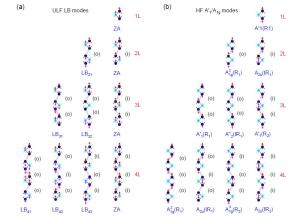
Two-dimensional transition metal dichalcogenides (TMDs) have attracted extensive attention due to their many novel properties. The atoms within each layer in two-dimensional TMDs are joined together by covalent bonds, while van der Waals interactions combine the layers together. This makes its lattice dynamics layer-number dependent. The evolutions of ultralow frequency (<50 cm-1) modes, such as shear and layer-breathing modes have been well-established. Here, we review the layer-number dependent high-frequency (>50 cm-1) vibration modes in few-layer TMDs and demonstrate how the interlayer coupling leads to the splitting of high-frequency vibration modes, known as Davydov splitting. Such Davydov splitting can be well described by a van der Waals model, which directly links the splitting with the interlayer coupling. Our review expands the understanding on the effect of interlayer coupling on the high-frequency vibration modes in TMDs and other two-dimensional materials.

Two-dimensional transition metal dichalcogenides (TMDs) have attracted extensive attention due to their many novel properties. The atoms within each layer in two-dimensional TMDs are joined together by covalent bonds, while van der Waals interactions combine the layers together. This makes its lattice dynamics layer-number dependent. The evolutions of ultralow frequency (<50 cm-1) modes, such as shear and layer-breathing modes have been well-established. Here, we review the layer-number dependent high-frequency (>50 cm-1) vibration modes in few-layer TMDs and demonstrate how the interlayer coupling leads to the splitting of high-frequency vibration modes, known as Davydov splitting. Such Davydov splitting can be well described by a van der Waals model, which directly links the splitting with the interlayer coupling. Our review expands the understanding on the effect of interlayer coupling on the high-frequency vibration modes in TMDs and other two-dimensional materials.
Effects of vertical electric field and compressive strain on electronic properties of bilayer ZrS2
Jimin Shang, Le Huang, Zhongming Wei
J. Semicond.  2017, 38(3): 033001  doi: 10.1088/1674-4926/38/3/033001

Using first-principles calculations, including Grimme D2 method for van der Waals interactions, we investigate the tuning electronic properties of bilayer zirconium disulfides (ZrS2) subjected to vertical electric field and normal compressive strain. The band gap of ZrS2 bilayer can be flexibly tuned by vertical external electric field. Due to the Stark effect, at critical electric fields about 1.4 V/Å, semiconducting-metallic transition presents. In addition, our results also demonstrated that the compressive strain has an important impact on the electronic properties of ZrS2 bilayer sheet. The widely tunable band gaps confirm possibilities for its applications in electronics and optoelectronics.

Using first-principles calculations, including Grimme D2 method for van der Waals interactions, we investigate the tuning electronic properties of bilayer zirconium disulfides (ZrS2) subjected to vertical electric field and normal compressive strain. The band gap of ZrS2 bilayer can be flexibly tuned by vertical external electric field. Due to the Stark effect, at critical electric fields about 1.4 V/Å, semiconducting-metallic transition presents. In addition, our results also demonstrated that the compressive strain has an important impact on the electronic properties of ZrS2 bilayer sheet. The widely tunable band gaps confirm possibilities for its applications in electronics and optoelectronics.
Ab initio electronic transport study of two-dimensional silicon carbide-based p-n junctions
Hanming Zhou, Xiao Lin, Hongwei Guo, Shisheng Lin, Yiwei Sun, Yang Xu
J. Semicond.  2017, 38(3): 033002  doi: 10.1088/1674-4926/38/3/033002

Two-dimensional silicon carbide (2d-SiC) is a viable material for next generation electronics due to its moderate, direct bandgap with huge potential. In particular, its potential for p-n junctions is yet to be explored. In this paper, three types of 2d-SiC-based p-n junctions with different doping configuration are modeled. The doping configurations refer to partially replacing carbon with boron or nitrogen atoms along the zigzag or armchair direction, respectively. By employing density functional theory, we calculate the transport properties of the SiC based p-n junctions and obtain negative differential resistance and high rectification ratio. We also find that the junction along the zigzag direction with lower doping density exhibits optimized rectification performance. Our study suggests that 2d-SiC is a promising candidate as a material platform for future nano-devices.

Two-dimensional silicon carbide (2d-SiC) is a viable material for next generation electronics due to its moderate, direct bandgap with huge potential. In particular, its potential for p-n junctions is yet to be explored. In this paper, three types of 2d-SiC-based p-n junctions with different doping configuration are modeled. The doping configurations refer to partially replacing carbon with boron or nitrogen atoms along the zigzag or armchair direction, respectively. By employing density functional theory, we calculate the transport properties of the SiC based p-n junctions and obtain negative differential resistance and high rectification ratio. We also find that the junction along the zigzag direction with lower doping density exhibits optimized rectification performance. Our study suggests that 2d-SiC is a promising candidate as a material platform for future nano-devices.
Investigation of multilayer domains in large-scale CVD monolayer graphene by optical imaging
Yuanfang Yu, Zhenzhen Li, Wenhui Wang, Xitao Guo, Jie Jiang, Haiyan Nan, Zhenhua Ni
J. Semicond.  2017, 38(3): 033003  doi: 10.1088/1674-4926/38/3/033003

CVD graphene is a promising candidate for optoelectronic applications due to its high quality and high yield. However, multi-layer domains could inevitably form at the nucleation centers during the growth. Here, we propose an optical imaging technique to precisely identify the multilayer domains and also the ratio of their coverage in large-scale CVD monolayer graphene. We have also shown that the stacking disorder in twisted bilayer graphene as well as the impurities on the graphene surface could be distinguished by optical imaging. Finally, we investigated the effects of bilayer domains on the optical and electrical properties of CVD graphene, and found that the carrier mobility of CVD graphene is seriously limited by scattering from bilayer domains. Our results could be useful for guiding future optoelectronic applications of large-scale CVD graphene.

CVD graphene is a promising candidate for optoelectronic applications due to its high quality and high yield. However, multi-layer domains could inevitably form at the nucleation centers during the growth. Here, we propose an optical imaging technique to precisely identify the multilayer domains and also the ratio of their coverage in large-scale CVD monolayer graphene. We have also shown that the stacking disorder in twisted bilayer graphene as well as the impurities on the graphene surface could be distinguished by optical imaging. Finally, we investigated the effects of bilayer domains on the optical and electrical properties of CVD graphene, and found that the carrier mobility of CVD graphene is seriously limited by scattering from bilayer domains. Our results could be useful for guiding future optoelectronic applications of large-scale CVD graphene.
Manganese and chromium doping in atomically thin MoS2
Ce Huang, Yibo Jin, Weiyi Wang, Lei Tang, Chaoyu Song, Faxian Xiu
J. Semicond.  2017, 38(3): 033004  doi: 10.1088/1674-4926/38/3/033004

Recently, two-dimensional materials have been attracting increasing attention because of their novel properties and promising applications. However, the impurity doping remains a significant challenge owing to the lack of the doping strategy in the atomically thin layers. Here we report on the chromium (Cr) and manganese (Mn) doping in atomically-thin MoS2 crystals grown by chemical vapor deposition. The Cr/Mn doped MoS2 samples are characterized by a peak at 1.76 and 1.79 eV in photoluminescence spectra, respectively, compared with the undoped one at 1.85 eV. The field-effect transistor (FET) devices based on the Mn doping show a higher threshold voltage than that of the pure MoS2 while the Cr doping exhibits the opposite behavior. Importantly, the carrier concentration in these samples displays a remarkable difference arising from the doping effect, consistent with the evolution of the FET performance. The temperature-dependent conductivity measurements further demonstrate a large variation in activation energy. The successful incorporation of the Mn and Cr impurities into the monolayer MoS2 paves the way towards the high Curie temperature two-dimensional dilute magnetic semiconductors.

Recently, two-dimensional materials have been attracting increasing attention because of their novel properties and promising applications. However, the impurity doping remains a significant challenge owing to the lack of the doping strategy in the atomically thin layers. Here we report on the chromium (Cr) and manganese (Mn) doping in atomically-thin MoS2 crystals grown by chemical vapor deposition. The Cr/Mn doped MoS2 samples are characterized by a peak at 1.76 and 1.79 eV in photoluminescence spectra, respectively, compared with the undoped one at 1.85 eV. The field-effect transistor (FET) devices based on the Mn doping show a higher threshold voltage than that of the pure MoS2 while the Cr doping exhibits the opposite behavior. Importantly, the carrier concentration in these samples displays a remarkable difference arising from the doping effect, consistent with the evolution of the FET performance. The temperature-dependent conductivity measurements further demonstrate a large variation in activation energy. The successful incorporation of the Mn and Cr impurities into the monolayer MoS2 paves the way towards the high Curie temperature two-dimensional dilute magnetic semiconductors.
Carbon-doping-induced negative differential resistance in armchair phosphorene nanoribbons
Caixia Guo, Congxin Xia, Tianxing Wang, Yufang Liu
J. Semicond.  2017, 38(3): 033005  doi: 10.1088/1674-4926/38/3/033005

By using a combined method of density functional theory and non-equilibrium Green's function formalism, we investigate the electronic transport properties of carbon-doped armchair phosphorene nanoribbons (APNRs). The results show that C atom doping can strongly affect the electronic transport properties of the APNR and change it from semiconductor to metal. Meanwhile, obvious negative differential resistance (NDR) behaviors are obtained by tuning the doping position and concentration. In particular, with reducing doping concentration, NDR peak position can enter into mV bias range. These results provide a theoretical support to design the related nanodevice by tuning the doping position and concentration in the APNRs.

By using a combined method of density functional theory and non-equilibrium Green's function formalism, we investigate the electronic transport properties of carbon-doped armchair phosphorene nanoribbons (APNRs). The results show that C atom doping can strongly affect the electronic transport properties of the APNR and change it from semiconductor to metal. Meanwhile, obvious negative differential resistance (NDR) behaviors are obtained by tuning the doping position and concentration. In particular, with reducing doping concentration, NDR peak position can enter into mV bias range. These results provide a theoretical support to design the related nanodevice by tuning the doping position and concentration in the APNRs.
Photoresponsive field-effect transistors based on multilayer SnS2 nanosheets
Yan Wang, Le Huang, Zhongming Wei
J. Semicond.  2017, 38(3): 034001  doi: 10.1088/1674-4926/38/3/034001

2D SnS2 nanosheets are exfoliated by micromechanical exfoliation technique from SnS2 single crystals which are synthesized by CVT methods. Monolayer SnS2 nanosheet has been obtained and the Raman spectrum shows that A1g mode of monolayer SnS2 shows a slight softening compared with bulk SnS2 single crystal. The field effect transistors (FETs) based on multilayer SnS2 nanosheets have been fabricated, of which the electrical and photoelectrical properties have been measured. Under dark condition, with Vsd of 1 V, our SnS2 FET shows n-type behavior. The carrier mobility of the FETs reach 3.51 cm2V-1s-1 and the ‘ON/OFF’ ratio is about 5×10². The SnS2 FET is also illuminated under 532 nm laser with the power of 500 mW/cm2. The light absorption causes an increment of carrier mobility (from 3.51 cm2V-1s-1 under dark condition to 3.85 cm2V-1s-1 under 532 nm laser illumination with the power of 500 mW/cm2) of SnS2. The responsivity (R) and detectivity of our multilayer device under 500 mW/cm2 532 nm is 2.08 A/W and 6×10⁶ J, respectively. All the above properties indicate the potential of SnS2 nanosheets to be used as FETs and phototransistors.

2D SnS2 nanosheets are exfoliated by micromechanical exfoliation technique from SnS2 single crystals which are synthesized by CVT methods. Monolayer SnS2 nanosheet has been obtained and the Raman spectrum shows that A1g mode of monolayer SnS2 shows a slight softening compared with bulk SnS2 single crystal. The field effect transistors (FETs) based on multilayer SnS2 nanosheets have been fabricated, of which the electrical and photoelectrical properties have been measured. Under dark condition, with Vsd of 1 V, our SnS2 FET shows n-type behavior. The carrier mobility of the FETs reach 3.51 cm2V-1s-1 and the ‘ON/OFF’ ratio is about 5×10². The SnS2 FET is also illuminated under 532 nm laser with the power of 500 mW/cm2. The light absorption causes an increment of carrier mobility (from 3.51 cm2V-1s-1 under dark condition to 3.85 cm2V-1s-1 under 532 nm laser illumination with the power of 500 mW/cm2) of SnS2. The responsivity (R) and detectivity of our multilayer device under 500 mW/cm2 532 nm is 2.08 A/W and 6×10⁶ J, respectively. All the above properties indicate the potential of SnS2 nanosheets to be used as FETs and phototransistors.
Enhancement of photodetection based on perovskite/MoS2 hybrid thin film transistor
Fengjing Liu, Jiawei Wang, Liang Wang, Xiaoyong Cai, Chao Jiang, Gongtang Wang
J. Semicond.  2017, 38(3): 034002  doi: 10.1088/1674-4926/38/3/034002

Perovskite/MoS2 hybrid thin film transistor photodetectors consist of few-layered MoS2 and CH3NH3PbI3 film with various thickness prepared by two-step vacuum deposition. By implementing perovskite CH3NH3PbI3 film onto the MoS2 flake, the perovskite/MoS2 hybrid photodetector exhibited a photoresponsivity of 104A/W and fast response time of about 40 ms. Improvement of photodetection performance is attributed to the balance between light absorption in the perovskite layer and an effective transfer of photogenerated carriers from perovskite entering the MoS2 channel. This work may provide guidance to develop high-performance hybrid structure optoelectronic devices.
Perovskite/MoS2 hybrid thin film transistor photodetectors consist of few-layered MoS2 and CH3NH3PbI3 film with various thickness prepared by two-step vacuum deposition. By implementing perovskite CH3NH3PbI3 film onto the MoS2 flake, the perovskite/MoS2 hybrid photodetector exhibited a photoresponsivity of 104A/W and fast response time of about 40 ms. Improvement of photodetection performance is attributed to the balance between light absorption in the perovskite layer and an effective transfer of photogenerated carriers from perovskite entering the MoS2 channel. This work may provide guidance to develop high-performance hybrid structure optoelectronic devices.
SEMICONDUCTOR MATERIALS
Progress of d0 magnetism in SiC
Yutian Wang, Chenguang Liu, Yuming Zhang
J. Semicond.  2017, 38(3): 033006  doi: 10.1088/1674-4926/38/3/033006

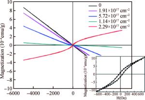
The properties of defect-induced ferromagnetism (d0 magnetism) in SiC belong to carbon-based material which has been systematically investigated after graphite. In this paper, we reviewed our research progress about d0 magnetism in two aspects, i.e., magnetic source and magnetic coupling mechanism. The VSiVC divacancies have been evidenced as the probable source of d0 magnetism in SiC. To trace the ferromagnetic source in microscopic and electronic view, the p electrons of the nearest-neighbor carbon atoms, which are around the VSiVC divacancies, are sourced. For magnetic coupling mechanism, a higher divacancy concentration leads to stronger paramagnetic interaction but not stronger ferromagnetic coupling. So the d0 magnetism can probably be explained as a local effect which is incapable of scaling up with the volume.
The properties of defect-induced ferromagnetism (d0 magnetism) in SiC belong to carbon-based material which has been systematically investigated after graphite. In this paper, we reviewed our research progress about d0 magnetism in two aspects, i.e., magnetic source and magnetic coupling mechanism. The VSiVC divacancies have been evidenced as the probable source of d0 magnetism in SiC. To trace the ferromagnetic source in microscopic and electronic view, the p electrons of the nearest-neighbor carbon atoms, which are around the VSiVC divacancies, are sourced. For magnetic coupling mechanism, a higher divacancy concentration leads to stronger paramagnetic interaction but not stronger ferromagnetic coupling. So the d0 magnetism can probably be explained as a local effect which is incapable of scaling up with the volume.
Colloidal synthesis and characterization of Cu2ZnSnS4 nanoplates
S. Ananthakumar, J. Ram Kumar, S. Moorthy Babu
J. Semicond.  2017, 38(3): 033007  doi: 10.1088/1674-4926/38/3/033007

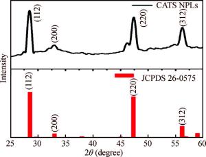
Synthesis of copper zinc tin sulphide (Cu2ZnSnS4) with nanoplate morphology was achieved through colloidal method using oleic acid as capping agent and solvent with 1-octadecene (1-ODE) at 240℃. X-ray diffraction (XRD) analysis shows that the synthesized nanoplates possessed pure kesterite phase. SEM analysis clearly shows the formation of nanoplates having the size of about 50-100 nm. Electron spin resonance (ESR) spectrum analysis of the prepared nanoplates shows that the valence state of copper (Ⅱ) which indicates the strong coupling with other metal ions. Thermo gravimetric/differential thermal analysis (TG/DTA) analysis shows the weight loss of sample at 450℃ predicting the loss of capping ligands on the surface of the nanoparticles. The possible mechanism for the conversion of nanoplate-like structures during synthesis was discussed. The results are discussed in detail.
Synthesis of copper zinc tin sulphide (Cu2ZnSnS4) with nanoplate morphology was achieved through colloidal method using oleic acid as capping agent and solvent with 1-octadecene (1-ODE) at 240℃. X-ray diffraction (XRD) analysis shows that the synthesized nanoplates possessed pure kesterite phase. SEM analysis clearly shows the formation of nanoplates having the size of about 50-100 nm. Electron spin resonance (ESR) spectrum analysis of the prepared nanoplates shows that the valence state of copper (Ⅱ) which indicates the strong coupling with other metal ions. Thermo gravimetric/differential thermal analysis (TG/DTA) analysis shows the weight loss of sample at 450℃ predicting the loss of capping ligands on the surface of the nanoparticles. The possible mechanism for the conversion of nanoplate-like structures during synthesis was discussed. The results are discussed in detail.
SEMICONDUCTOR INTEGRATED CIRCUITS
A 77-100 GHz power amplifier using 0.1-μm GaAs PHEMT technology
Qin Ge, Wei Liu, Bo Xu, Feng Qian, Changfei Yao
J. Semicond.  2017, 38(3): 035001  doi: 10.1088/1674-4926/38/3/035001

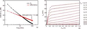
A wideband MMIC power amplifier at W-band is reported in this letter. The four-stage MMIC, developed using 0.1 μm GaAs pseudomorphic HEMT (PHEMT) technology, demonstrated a flat small signal gain of 12.4±2 dB with a minimum saturated output power (Psat) of 14.2 dBm from 77 to 100 GHz. The typical Psat is better by 16.3 dBm with a flatness of 0.4 dB and the maximum power added efficiency is 6% between 77 and 92 GHz. This result shows that the amplifier delivers output power density of about 470 mW/mm with a total gate output periphery of 100 μm. As far as we know, it is nearly the best power density performance ever published from a single ended GaAs-based PHEMT MMIC at this frequency band.
A wideband MMIC power amplifier at W-band is reported in this letter. The four-stage MMIC, developed using 0.1 μm GaAs pseudomorphic HEMT (PHEMT) technology, demonstrated a flat small signal gain of 12.4±2 dB with a minimum saturated output power (Psat) of 14.2 dBm from 77 to 100 GHz. The typical Psat is better by 16.3 dBm with a flatness of 0.4 dB and the maximum power added efficiency is 6% between 77 and 92 GHz. This result shows that the amplifier delivers output power density of about 470 mW/mm with a total gate output periphery of 100 μm. As far as we know, it is nearly the best power density performance ever published from a single ended GaAs-based PHEMT MMIC at this frequency band.
A high EMS daisy-chain SPI interface for battery monitor system
Qidong Zhang, Yintang Yang, Changchun Chai
J. Semicond.  2017, 38(3): 035002  doi: 10.1088/1674-4926/38/3/035002

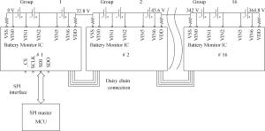
A high EMS current-mode SPI interface for battery monitor IC (BMIC) is presented to form a daisy-chain bus configuration for the cascaded BMICs and the communication between the MCU and master BMIC. Based on analog and digital mixed filtering technique, the proposed daisy-chain can avoid the isolated communication issue in electromagnetic interference environment, and reduce the extensively required I/O ports of MCU, at the same time reduce the system cost. The proposed daisy-chain interface was introduced in a 6-ch battery monitor IC which was fabricated with 0.35 μm 30 V BCD process. The measurement result shows that the presented daisy-chain SPI interface achieves better EMS performance with different EMI injection while just consuming a total operation current up to 1 mA.

A high EMS current-mode SPI interface for battery monitor IC (BMIC) is presented to form a daisy-chain bus configuration for the cascaded BMICs and the communication between the MCU and master BMIC. Based on analog and digital mixed filtering technique, the proposed daisy-chain can avoid the isolated communication issue in electromagnetic interference environment, and reduce the extensively required I/O ports of MCU, at the same time reduce the system cost. The proposed daisy-chain interface was introduced in a 6-ch battery monitor IC which was fabricated with 0.35 μm 30 V BCD process. The measurement result shows that the presented daisy-chain SPI interface achieves better EMS performance with different EMI injection while just consuming a total operation current up to 1 mA.