SPECIAL TOPIC ON 2D MATERIALS AND DEVICES

Photoresponsive field-effect transistors based on multilayer SnS2 nanosheets

Yan Wang, Le Huang and Zhongming Wei

+ Author Affiliations

 Corresponding author: Yan Wang, Email:yanwang@semi.ac.cn

PDF

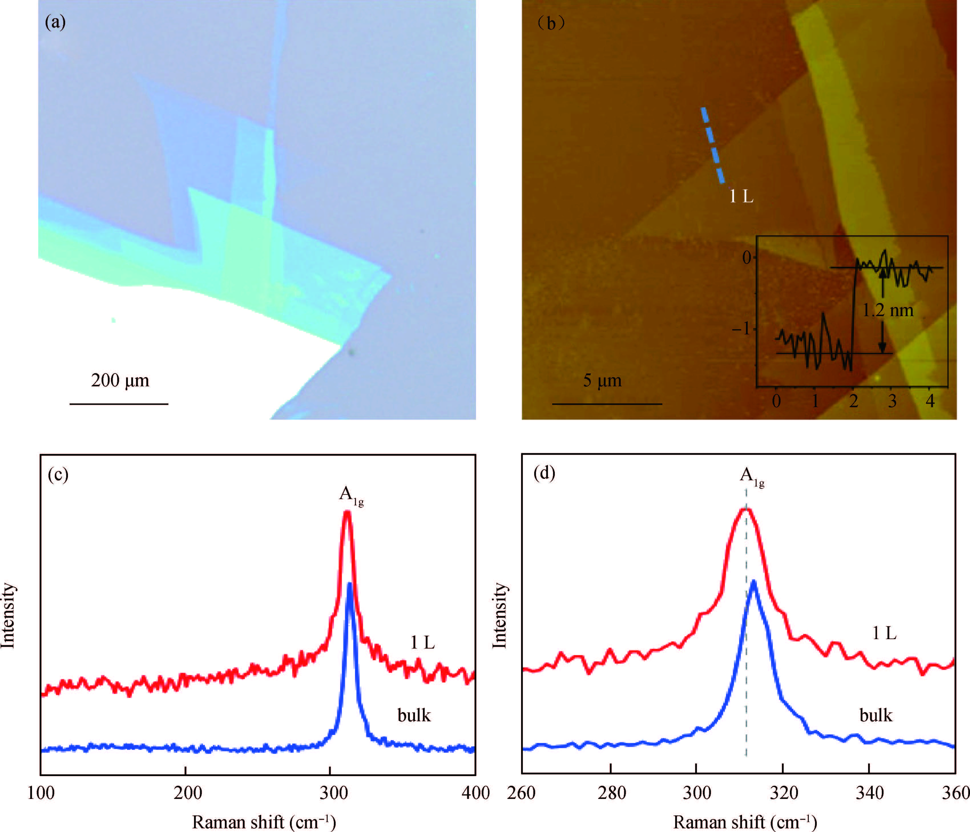
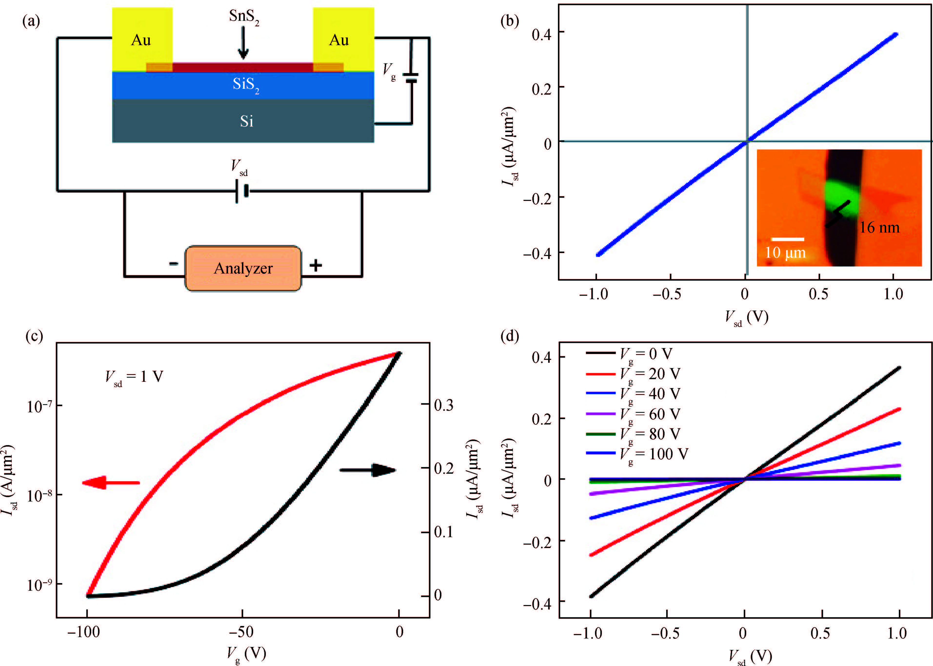
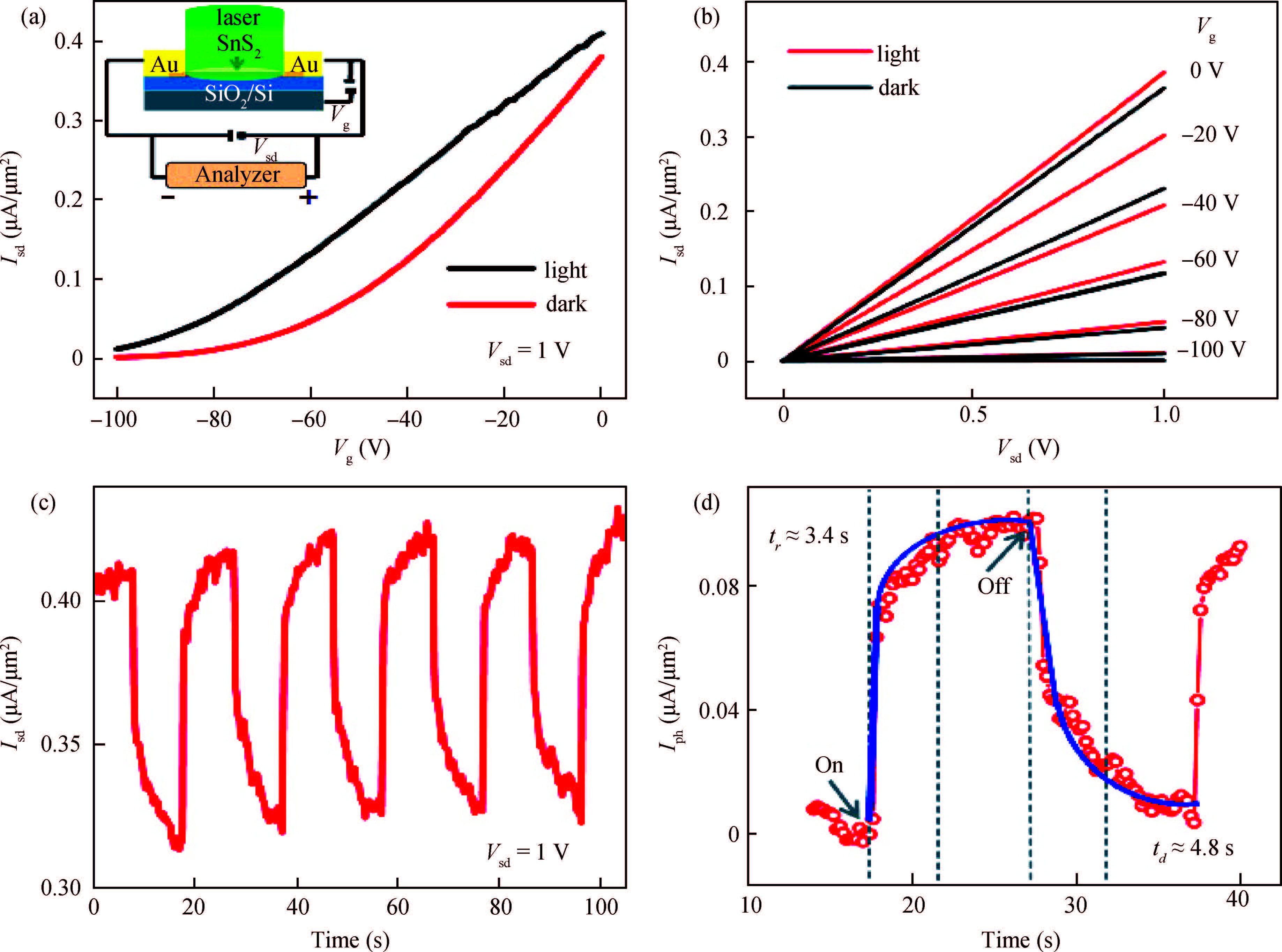
Abstract: 2D SnS2 nanosheets are exfoliated by micromechanical exfoliation technique from SnS2 single crystals which are synthesized by CVT methods. Monolayer SnS2 nanosheet has been obtained and the Raman spectrum shows that A1g mode of monolayer SnS2 shows a slight softening compared with bulk SnS2 single crystal. The field effect transistors (FETs) based on multilayer SnS2 nanosheets have been fabricated, of which the electrical and photoelectrical properties have been measured. Under dark condition, with Vsd of 1 V, our SnS2 FET shows n-type behavior. The carrier mobility of the FETs reach 3.51 cm2V-1s-1 and the ‘ON/OFF’ ratio is about 5×10². The SnS2 FET is also illuminated under 532 nm laser with the power of 500 mW/cm2. The light absorption causes an increment of carrier mobility (from 3.51 cm2V-1s-1 under dark condition to 3.85 cm2V-1s-1 under 532 nm laser illumination with the power of 500 mW/cm2) of SnS2. The responsivity (R) and detectivity of our multilayer device under 500 mW/cm2 532 nm is 2.08 A/W and 6×10⁶ J, respectively. All the above properties indicate the potential of SnS2 nanosheets to be used as FETs and phototransistors.

Key words: two-dimensional materialsTMDsSnS2


[1]
Schwierz F. Graphene transistors. Nat Nanotechnol, 2010, 5(7):487 doi: 10.1038/nnano.2010.89
[2]
Geim A K. Graphene:status and prospects. Science, 2009, 324(5934):1530 doi: 10.1126/science.1158877
[3]
Avouris P, Chen Z, Perebeinos V. Carbon-based electronics. Nat Nanotechnol, 2007, 2(10):605 doi: 10.1038/nnano.2007.300
[4]
Novoselov K S, Geim A K, Morozov S V, et al. Electric field effect in atomically thin carbon films. Science, 2004, 306(5696):666 doi: 10.1126/science.1102896
[5]
Chen F, Xia J L, Ferry D K, et al. Dielectric screening enhanced performance in graphene FET. Nano Lett, 2009, 9(7):2571 doi: 10.1021/nl900725u
[6]
Schedin F, Geim A K, Morozov S V, et al. Detection of individual gas molecules adsorbed on graphene. Nat Mater, 2007, 6(9):652 doi: 10.1038/nmat1967
[7]
Das S, Robinson J A, Dubey M, et al. Beyond graphene:progress in novel two-dimensional materials and van der Waals solids. Ann Rev Mater Res, 2015, 45:1 doi: 10.1146/annurev-matsci-070214-021034
[8]
Lee Y H, Yu L L, Wang H, et al. Synthesis and transfer of singlelayer transition metal disulfides on diverse surfaces. Nano Lett, 2013, 13(4):1852 doi: 10.1021/nl400687n
[9]
Wang Q H, Kalantar-Zadeh K, Kis A, et al. Electronics and optoelectronics of two-dimensional transition metal dichalcogenides. Nat Nanotech, 2012, 7(11):699 doi: 10.1038/nnano.2012.193
[10]
Wang F, Wang Z X, Wang Q S, et al. Synthesis, properties and applications of 2D non-graphene materials. Nanotechnology, 2015, 26(29):26 https://www.researchgate.net/publication/279730603_Synthesis_properties_and_applications_of_2D_non-graphene_materials
[11]
Elias A L, Perea-Lopez N, Castro-Beltran A, et al. Controlled synthesis and transfer of large-area WS2 sheets:from single layer to few layers. ACS Nano, 2013, 7(6):5235 doi: 10.1021/nn400971k
[12]
Hwang W S, Remskar M, Yan R S, et al. Transistors with chemically synthesized layered semiconductor WS2 exhibiting 105 room temperature modulation and ambipolar behavior. Appl Phys Lett, 2012, 101(1):4 http://www.oalib.com/paper/3325833
[13]
Podzorov V, Gershenson M E, Kloc C, et al. High-mobility fieldeffect transistors based on transition metal dichalcogenides. Appl Phys Lett, 2004, 84(17):3301 doi: 10.1063/1.1723695
[14]
Fang H, Chuang S, Chang T C, et al. High-performance single layered WSe2 p-FETs with chemically doped contacts. Nano Lett, 2012, 12(7):3788 doi: 10.1021/nl301702r
[15]
Tsai D S, Liu K K, Lien D H, et al. Few-layer MoS2 with high broadband photogain and fast optical switching for use in harsh environments. ACS Nano, 2013, 7(5):3905 doi: 10.1021/nn305301b
[16]
Radisavljevic B, Radenovic A, Brivio J, et al. Single-layer MoS2 transistors. Nat Nanotechnol, 2011, 6(3):147 doi: 10.1038/nnano.2010.279
[17]
Lopez-Sanchez O, Lembke D, Kayci M, et al. Ultrasensitive photodetectors based on monolayer MoS2. Nat Nanotech, 2013, 8(7):497 doi: 10.1038/nnano.2013.100
[18]
Yue Q, Shao Z Z, Chang S L, et al. Adsorption of gas molecules on monolayer MoS2 and effect of applied electric field. Nanoscale Res Lett, 2013, 8:7 doi: 10.1186/1556-276X-8-7
[19]
He Q Y, Zeng Z Y, Yin Z Y, et al. Fabrication of flexible MoS2 thin-film transistor arrays for practical gas-sensing applications. Small, 2012, 8(19):2994 doi: 10.1002/smll.v8.19
[20]
Lopez-Sanchez O, Lembke D, Kayci M, et al. Ultrasensitive photodetectors based on monolayer MoS2. Nat Nanotechnol, 2013, 8(7):497 doi: 10.1038/nnano.2013.100
[21]
Su G, Hadjiev V G, Loya P E, et al. Chemical vapor deposition of thin crystals of layered semiconductor SnS2 for fast photodetection application. Nano Lett, 2015, 15(1):506 doi: 10.1021/nl503857r
[22]
Ricica T, Strizik L, Dostal L, et al. SnS and SnS2 thin films deposited using a spin-coating technique from intramolecularly coordinated organotin sulfides. Appl Organomet Chem, 2015, 29(3):176 doi: 10.1002/aoc.v29.3
[23]
Kiruthigaa G, Manoharan C, Bououdina M, et al. Structural, optical and photocatalytic properties of Ce-doped SnS2 nanoflakes. Solid State Sci, 2015, 44:32 doi: 10.1016/j.solidstatesciences.2015.04.003
[24]
Ahn J H, Lee M J, Heo H, et al. Deterministic two-dimensional polymorphism growth of hexagonal n-type SnS2 and orthorhombic p-type SnS crystals. Nano Lett, 2015, 15(6):3703 doi: 10.1021/acs.nanolett.5b00079
[25]
Kiruthigaa G, Manoharan C, Raju C, et al. Solid state synthesis and spectral investigations of nanostructure SnS2. Spectroc Acta A, 2014, 129:415 doi: 10.1016/j.saa.2014.03.088
[26]
Li H, Zhang Q, Yap C C R, et al. From bulk to monolayer MoS2:evolution of Raman scattering. Adv Funct Mater, 2012, 22(7):1385 doi: 10.1002/adfm.v22.7
[27]
Tonndorf P, Schmidt R, Bottger P, et al. Photoluminescence emission and Raman response of monolayer MoS2, MoSe2, and WSe2. Opt Express, 2013, 21(4):4908 doi: 10.1364/OE.21.004908
[28]
Wang Q, Li J, Lei Y, et al. Oriented growth of Pb1-xSnxTe nanowire arrays for integration of flexible infrared detectors. Adv Mater, 2015, 28(18):3596
[29]
Wang X, Wang P, Wang J, et al. Ultrasensitive and broadband MoS2 photodetector driven by ferroelectrics. Adv Mater, 2015, 27(42):6575 doi: 10.1002/adma.201503340
[30]
Xu K, Wang Z, Wang F, et al. Ultrasensitive phototransistors based on few-layered HfS2. Adv Mater, 2015, 27(47):7881 doi: 10.1002/adma.201503864
[31]
Zhong M, Wei Z, Meng X, et al. High-performance single crystalline UV photodetectors of β-Ga2O3. J Alloys Compd, 2015, 619:572 doi: 10.1016/j.jallcom.2014.09.070
Fig. 1.  (Color online) (a) Optical and (b) AFM image of SnS2 nanosheets. Inset in panel (b) is the height profile along the blue dotted line in (b), the thickness of monolayer SnS2 measured by AFM is about 1.2 nm, larger than the theoretical interlayer distance in SnS2 bulk materials (~ 0.7 nm), which can be attributed to the instrumental offset. (c) and (d) Raman spectra of SnS2 monolayer (red line) and bulk samples (blue line).

Fig. 2.  (a) Typical TEM image. (b) SAED pattern. (c) Its HRTEM image.

Fig. 3.  (Color online) (a) Schematic diagram of SnS2 transistor device and the typical measurement setup. (b) I-V (Isd-Vsd) curve of the transistor, which indicates the Ohmic contact between the SnS2 nanosheet and the Au electrode. Inset of (b) is the optical image of multilayers SnS2 device, the nanosheet thickness of which is about 16 nm from AFM result. (c) Transfer (Isd-Vg) and (d) output (Isd-Vsd) characteristics of SnS2 transistor.

Fig. 4.  (Color online) (a) Transfer (Isd-Vg) and (b) output (Isd-Vsd) characteristics of SnS2 FETs measured under dark and laser power of 500 mW/cm2. The inset of (a) is the schematic diagram of SnS2 transistor device and the typical measurement setup under light illumination. (c) Time dependences of Isd with Vsd= 1 V during the incident light switched on/off. (d) One magnified circle of the photoresponse curve in (c) with rising time of 3.4 s and decay time of 4.8 s.

[1]
Schwierz F. Graphene transistors. Nat Nanotechnol, 2010, 5(7):487 doi: 10.1038/nnano.2010.89
[2]
Geim A K. Graphene:status and prospects. Science, 2009, 324(5934):1530 doi: 10.1126/science.1158877
[3]
Avouris P, Chen Z, Perebeinos V. Carbon-based electronics. Nat Nanotechnol, 2007, 2(10):605 doi: 10.1038/nnano.2007.300
[4]
Novoselov K S, Geim A K, Morozov S V, et al. Electric field effect in atomically thin carbon films. Science, 2004, 306(5696):666 doi: 10.1126/science.1102896
[5]
Chen F, Xia J L, Ferry D K, et al. Dielectric screening enhanced performance in graphene FET. Nano Lett, 2009, 9(7):2571 doi: 10.1021/nl900725u
[6]
Schedin F, Geim A K, Morozov S V, et al. Detection of individual gas molecules adsorbed on graphene. Nat Mater, 2007, 6(9):652 doi: 10.1038/nmat1967
[7]
Das S, Robinson J A, Dubey M, et al. Beyond graphene:progress in novel two-dimensional materials and van der Waals solids. Ann Rev Mater Res, 2015, 45:1 doi: 10.1146/annurev-matsci-070214-021034
[8]
Lee Y H, Yu L L, Wang H, et al. Synthesis and transfer of singlelayer transition metal disulfides on diverse surfaces. Nano Lett, 2013, 13(4):1852 doi: 10.1021/nl400687n
[9]
Wang Q H, Kalantar-Zadeh K, Kis A, et al. Electronics and optoelectronics of two-dimensional transition metal dichalcogenides. Nat Nanotech, 2012, 7(11):699 doi: 10.1038/nnano.2012.193
[10]
Wang F, Wang Z X, Wang Q S, et al. Synthesis, properties and applications of 2D non-graphene materials. Nanotechnology, 2015, 26(29):26 https://www.researchgate.net/publication/279730603_Synthesis_properties_and_applications_of_2D_non-graphene_materials
[11]
Elias A L, Perea-Lopez N, Castro-Beltran A, et al. Controlled synthesis and transfer of large-area WS2 sheets:from single layer to few layers. ACS Nano, 2013, 7(6):5235 doi: 10.1021/nn400971k
[12]
Hwang W S, Remskar M, Yan R S, et al. Transistors with chemically synthesized layered semiconductor WS2 exhibiting 105 room temperature modulation and ambipolar behavior. Appl Phys Lett, 2012, 101(1):4 http://www.oalib.com/paper/3325833
[13]
Podzorov V, Gershenson M E, Kloc C, et al. High-mobility fieldeffect transistors based on transition metal dichalcogenides. Appl Phys Lett, 2004, 84(17):3301 doi: 10.1063/1.1723695
[14]
Fang H, Chuang S, Chang T C, et al. High-performance single layered WSe2 p-FETs with chemically doped contacts. Nano Lett, 2012, 12(7):3788 doi: 10.1021/nl301702r
[15]
Tsai D S, Liu K K, Lien D H, et al. Few-layer MoS2 with high broadband photogain and fast optical switching for use in harsh environments. ACS Nano, 2013, 7(5):3905 doi: 10.1021/nn305301b
[16]
Radisavljevic B, Radenovic A, Brivio J, et al. Single-layer MoS2 transistors. Nat Nanotechnol, 2011, 6(3):147 doi: 10.1038/nnano.2010.279
[17]
Lopez-Sanchez O, Lembke D, Kayci M, et al. Ultrasensitive photodetectors based on monolayer MoS2. Nat Nanotech, 2013, 8(7):497 doi: 10.1038/nnano.2013.100
[18]
Yue Q, Shao Z Z, Chang S L, et al. Adsorption of gas molecules on monolayer MoS2 and effect of applied electric field. Nanoscale Res Lett, 2013, 8:7 doi: 10.1186/1556-276X-8-7
[19]
He Q Y, Zeng Z Y, Yin Z Y, et al. Fabrication of flexible MoS2 thin-film transistor arrays for practical gas-sensing applications. Small, 2012, 8(19):2994 doi: 10.1002/smll.v8.19
[20]
Lopez-Sanchez O, Lembke D, Kayci M, et al. Ultrasensitive photodetectors based on monolayer MoS2. Nat Nanotechnol, 2013, 8(7):497 doi: 10.1038/nnano.2013.100
[21]
Su G, Hadjiev V G, Loya P E, et al. Chemical vapor deposition of thin crystals of layered semiconductor SnS2 for fast photodetection application. Nano Lett, 2015, 15(1):506 doi: 10.1021/nl503857r
[22]
Ricica T, Strizik L, Dostal L, et al. SnS and SnS2 thin films deposited using a spin-coating technique from intramolecularly coordinated organotin sulfides. Appl Organomet Chem, 2015, 29(3):176 doi: 10.1002/aoc.v29.3
[23]
Kiruthigaa G, Manoharan C, Bououdina M, et al. Structural, optical and photocatalytic properties of Ce-doped SnS2 nanoflakes. Solid State Sci, 2015, 44:32 doi: 10.1016/j.solidstatesciences.2015.04.003
[24]
Ahn J H, Lee M J, Heo H, et al. Deterministic two-dimensional polymorphism growth of hexagonal n-type SnS2 and orthorhombic p-type SnS crystals. Nano Lett, 2015, 15(6):3703 doi: 10.1021/acs.nanolett.5b00079
[25]
Kiruthigaa G, Manoharan C, Raju C, et al. Solid state synthesis and spectral investigations of nanostructure SnS2. Spectroc Acta A, 2014, 129:415 doi: 10.1016/j.saa.2014.03.088
[26]
Li H, Zhang Q, Yap C C R, et al. From bulk to monolayer MoS2:evolution of Raman scattering. Adv Funct Mater, 2012, 22(7):1385 doi: 10.1002/adfm.v22.7
[27]
Tonndorf P, Schmidt R, Bottger P, et al. Photoluminescence emission and Raman response of monolayer MoS2, MoSe2, and WSe2. Opt Express, 2013, 21(4):4908 doi: 10.1364/OE.21.004908
[28]
Wang Q, Li J, Lei Y, et al. Oriented growth of Pb1-xSnxTe nanowire arrays for integration of flexible infrared detectors. Adv Mater, 2015, 28(18):3596
[29]
Wang X, Wang P, Wang J, et al. Ultrasensitive and broadband MoS2 photodetector driven by ferroelectrics. Adv Mater, 2015, 27(42):6575 doi: 10.1002/adma.201503340
[30]
Xu K, Wang Z, Wang F, et al. Ultrasensitive phototransistors based on few-layered HfS2. Adv Mater, 2015, 27(47):7881 doi: 10.1002/adma.201503864
[31]
Zhong M, Wei Z, Meng X, et al. High-performance single crystalline UV photodetectors of β-Ga2O3. J Alloys Compd, 2015, 619:572 doi: 10.1016/j.jallcom.2014.09.070
  • Search

    Advanced Search >>

    GET CITATION

    shu

    Export: BibTex EndNote

    Article Metrics

    Article views: 4737 Times PDF downloads: 52 Times Cited by: 0 Times

    History

    Received: 27 September 2016 Revised: 27 October 2016 Online: Published: 01 March 2017

    Catalog

      Email This Article

      User name:
      Email:*请输入正确邮箱
      Code:*验证码错误
      Yan Wang, Le Huang, Zhongming Wei. Photoresponsive field-effect transistors based on multilayer SnS2 nanosheets[J]. Journal of Semiconductors, 2017, 38(3): 034001. doi: 10.1088/1674-4926/38/3/034001 ****Y Wang, L Huang, Z M Wei. Photoresponsive field-effect transistors based on multilayer SnS2 nanosheets[J]. J. Semicond., 2017, 38(3): 034001. doi: 10.1088/1674-4926/38/3/034001.
      Citation:
      Yan Wang, Le Huang, Zhongming Wei. Photoresponsive field-effect transistors based on multilayer SnS2 nanosheets[J]. Journal of Semiconductors, 2017, 38(3): 034001. doi: 10.1088/1674-4926/38/3/034001 ****
      Y Wang, L Huang, Z M Wei. Photoresponsive field-effect transistors based on multilayer SnS2 nanosheets[J]. J. Semicond., 2017, 38(3): 034001. doi: 10.1088/1674-4926/38/3/034001.

      Photoresponsive field-effect transistors based on multilayer SnS2 nanosheets

      doi: 10.1088/1674-4926/38/3/034001
      More Information
      • Corresponding author: Email:yanwang@semi.ac.cn
      • Received Date: 2016-09-27
      • Revised Date: 2016-10-27
      • Published Date: 2017-03-01

      Catalog

        /

        DownLoad:  Full-Size Img  PowerPoint
        Return
        Return