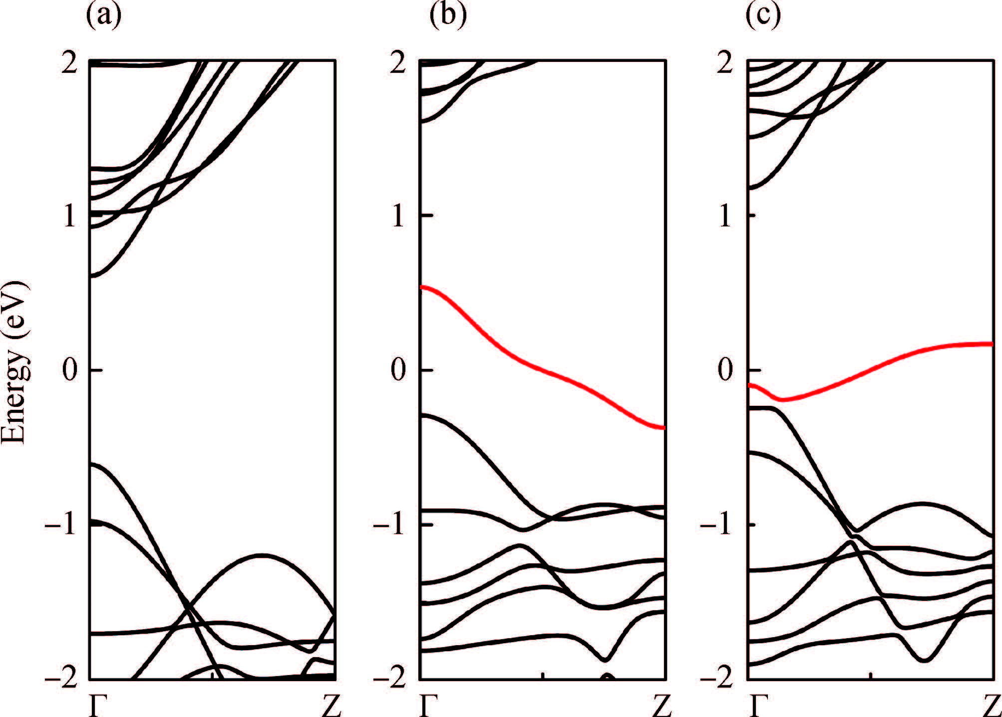
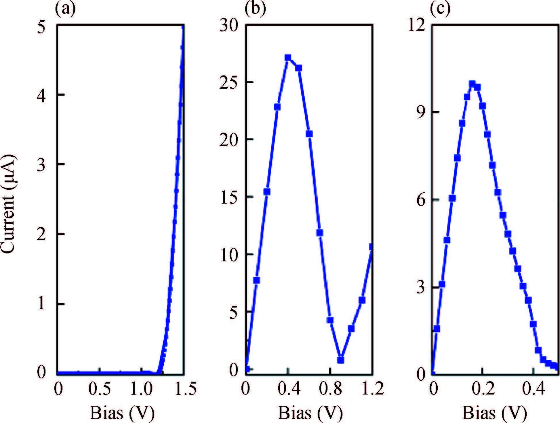
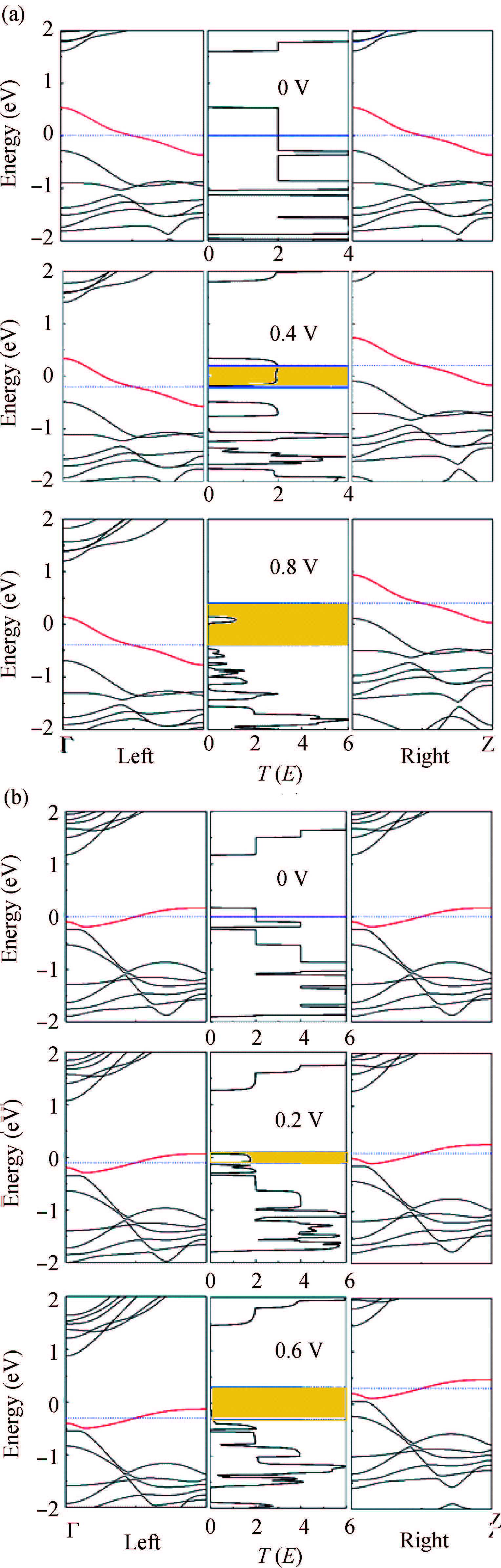
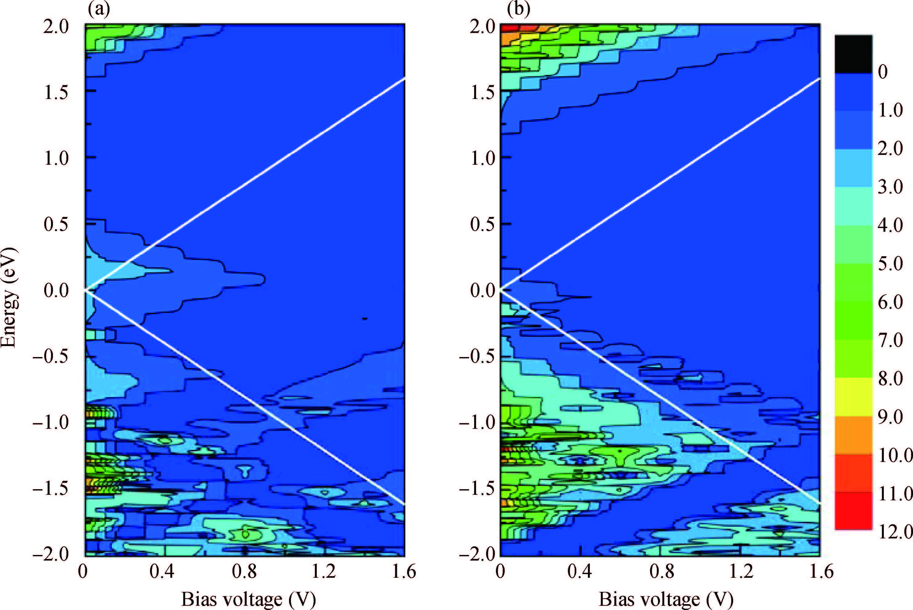
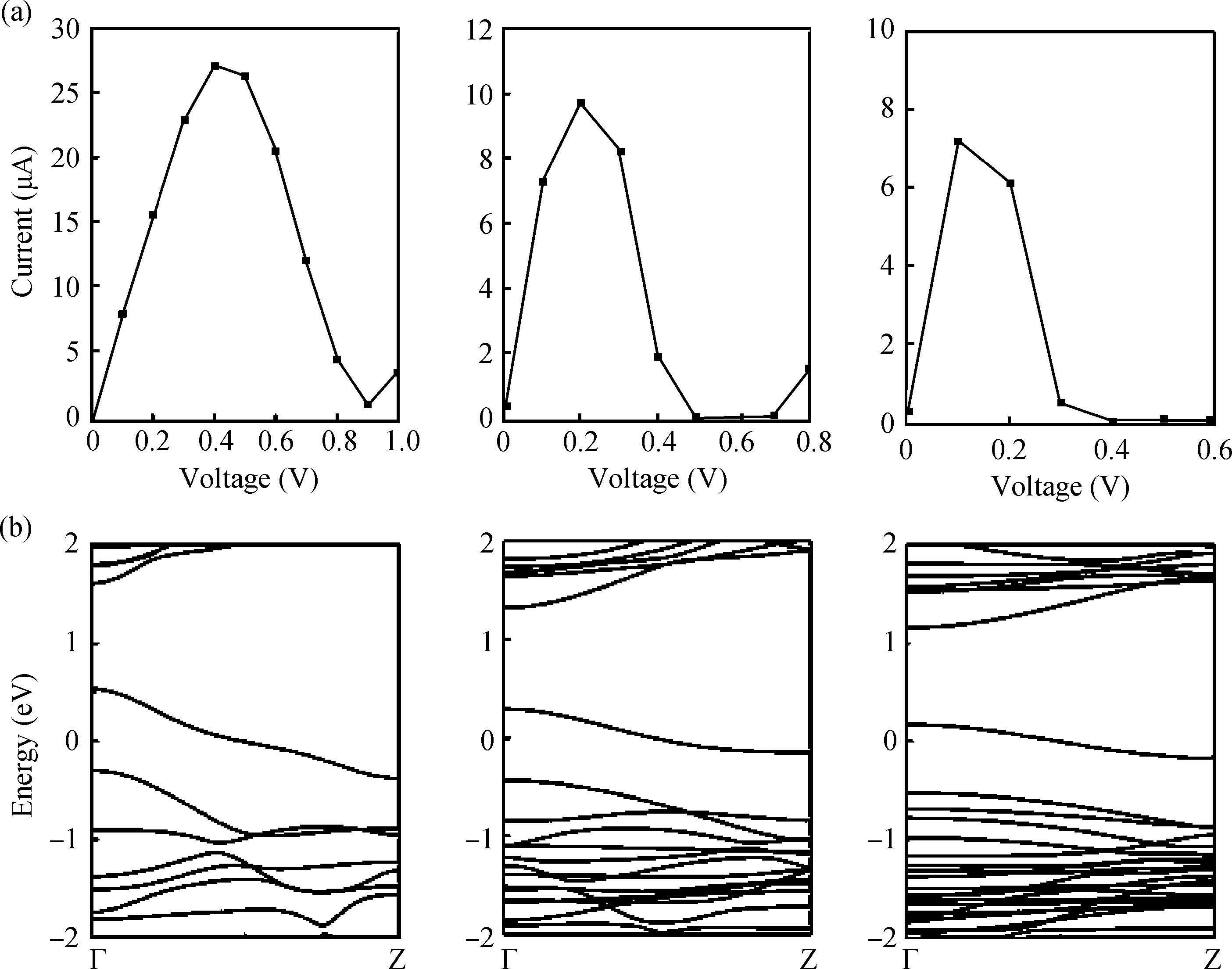
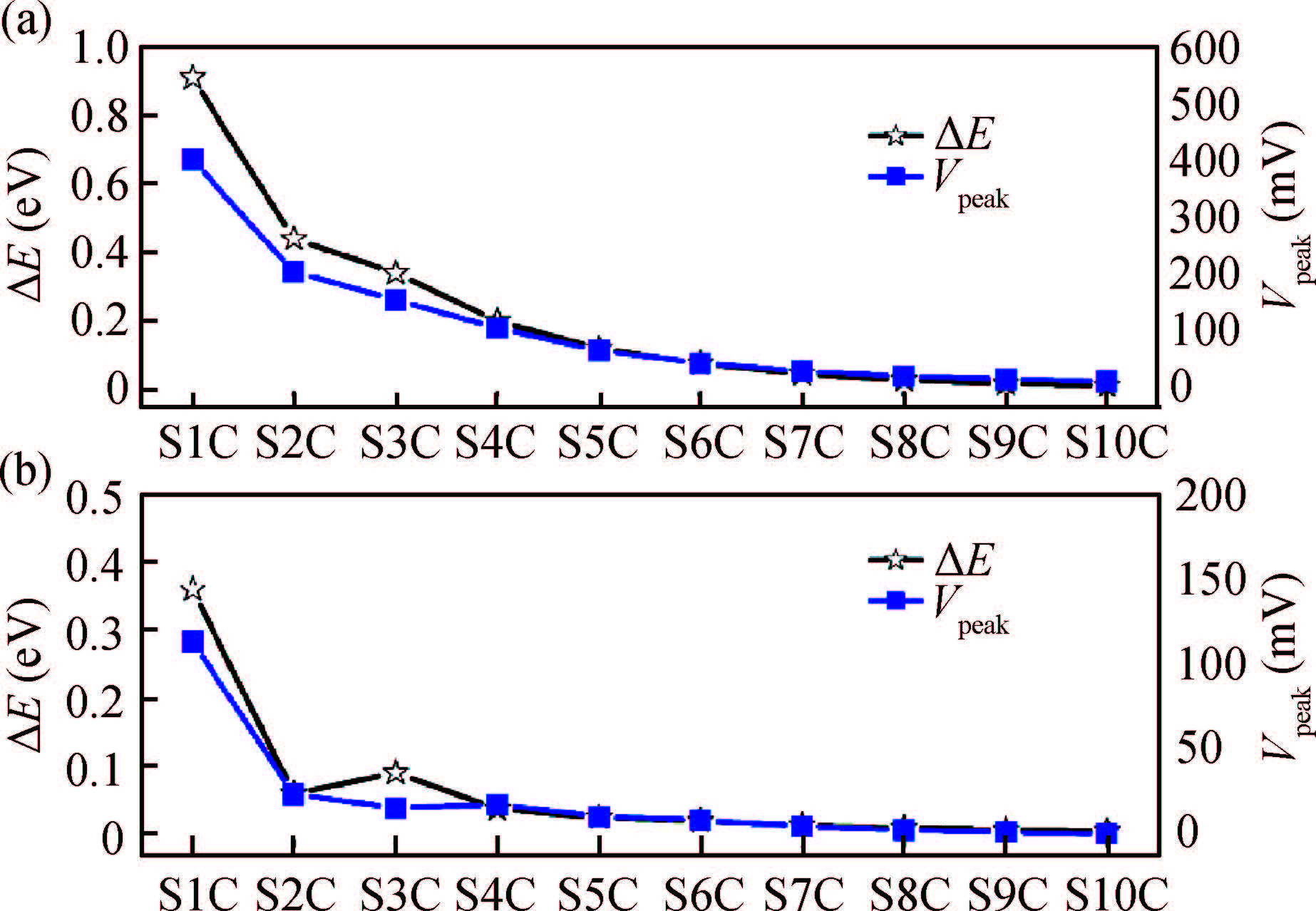
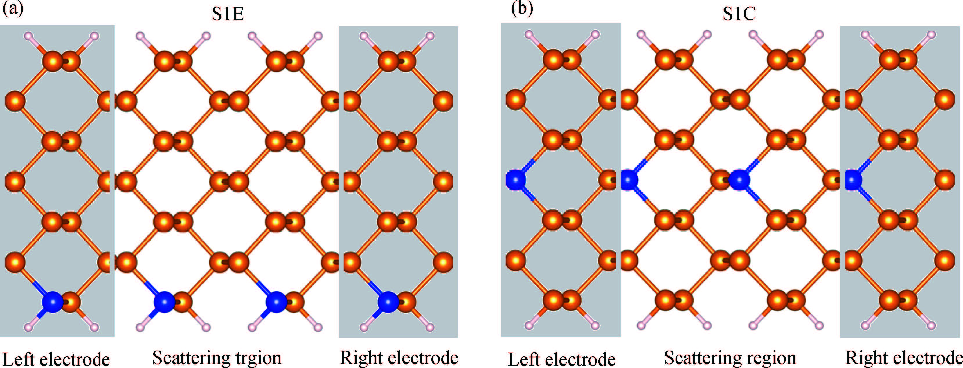
J. Semicond. > 2017, Volume 38 > Issue 3 > 033005

SPECIAL TOPIC ON 2D MATERIALS AND DEVICES

Carbon-doping-induced negative differential resistance in armchair phosphorene nanoribbons

Caixia Guo, Congxin Xia, Tianxing Wang and Yufang Liu

+ Author Affiliations

 Corresponding author: Congxin Xia, Email:xiacongxin@htu.edu.cn

DOI: 10.1088/1674-4926/38/3/033005

PDF

Abstract: By using a combined method of density functional theory and non-equilibrium Green's function formalism, we investigate the electronic transport properties of carbon-doped armchair phosphorene nanoribbons (APNRs). The results show that C atom doping can strongly affect the electronic transport properties of the APNR and change it from semiconductor to metal. Meanwhile, obvious negative differential resistance (NDR) behaviors are obtained by tuning the doping position and concentration. In particular, with reducing doping concentration, NDR peak position can enter into mV bias range. These results provide a theoretical support to design the related nanodevice by tuning the doping position and concentration in the APNRs.

Key words: C atom dopingarmchair phosphorene nanoribbonnegative differential resistance behavior

The ring oscillator finds various applications in the range of GHz, and voltage-controlled oscillators have been widely using it. The limitation of LC oscillators is the larger chip area, as they require spiral inductors; in addition, the tuning range of LC oscillators is relatively smaller[1, 2]. In comparison with the LC oscillator, the frequency of operation of the ring oscillator depends on the stage delay of CMOS inverter. In turn, the stage delay of inverter depends on the RC model of MOSFETs. Fig. 1 shows the general diagram of a 3-stage ring oscillator.

Figure  1.  Gate level diagram of 3-stage ring oscillator.

With the ring oscillator, for the completion of one cycle, the propagating signal has to pass twice through the stages. By making use of the stage delay (td) and the no. of stages (N), the frequency of operation is conventionally expressed as

fosc=12Ntd.
(1)

For operating in the range of gigahertz, the ring oscillator does not require any external RC components, as the MOSFET itself provides the parasitic components. Thus, the stage delay is the same as the inverter delay[3]. In order to obtain the inverter delay, the gate capacitance of the inverter is utilized for the purpose of modeling. One method of computing the delay is in terms of the effective capacitance and the switching current[4, 5].

td=CtotalVddID.
(2)

This model includes the Miller capacitance effect, and hence is useful for the designer[6, 7]. But the limitation is that, with reference to the switching transition, this model yields the total capacitance, Ctot = 2.5(COXp + COXn), and the current or resistance calculations have to be performed by the designer alone[8, 9]. In addition, the submicron parasitic effects are ignored in this model, as it is primarily meant for the micrometer dimensions.

In this paper, an effort has been made to overcome the limitations mentioned above. The paper is organized as follows. Section 2 considers the parasitic switching effects, and deals with the RC switching model of the ring oscillator. In Section 3, the derivation of an equation for the oscillating frequency is discussed, based on the model proposed in the previous section. In Section 4, the circuit simulation results and the verification of the derived equation are elaborated. Finally, Section 5 concludes the results obtained.

In the BSIM 4V4.8.0 SPICE model, for each type of MOSFET, there are more than 200 parameters. Hence for the manual calculations, it is not possible for the circuit designer, to make use of these many parameters. The primary purpose of these parameters is to aid in the characterization of devices for the purpose of simulation[10, 11]. Hence, during the design of CMOS ring oscillators in the submicron technology nodes, it is preferable to use the design equations of the first order, keeping the second order effects in mind. An effort is made in this work, to arrive at an equation for the oscillating frequency of the ring oscillator, in terms of the dimensions of the device. The modeling of the switching transistors is performed after considering the submicron switching behavior of the devices. The circuit diagram is shown in Fig. 2 for a 3-stage ring oscillator, and Fig. 3 shows the RC model.

Figure  2.  Circuit diagram of 3-stage CMOS ring oscillator.

The initial input to PM1 and NM1 is considered as “0”, and the RC model is constructed as shown in Fig. 3. The channel resistances for p and n type MOSFETs are represented as RSDp and RDSn, and the gate capacitances for the same are represented as CGp and CGn. In addition, the drain capacitances with respect to the body are shown as CDBp and CDBn. These parasitic capacitances are also called junction capacitances or diffusion capacitances. As the NMOS source is connected to ground and PMOS source is connected to VDD, the parasitic source capacitances with respect to the body or substrate are ignored.

For the purpose of arriving at the frequency of operation, the stage delay can be modeled in terms of the transitions at the output, i.e., low-to-high and high-to-low. As the output of the ring oscillator does not contain any steady logic state of ‘0’ or ‘1’, the stage delay can be expressed using the time constants, τPLH and τPHL. Thus,

td=τpLH+τpHL.
(3)

Hence, Eq. (1) gets modified as,

fosc=12N(τpLH+τpHL).
(4)

The first order equations for the transistors are chiefly utilized for micrometer dimensions, and they are not accurate in the nanometer dimensions. But, as the BSIM 4V4.8.0 SPICE model contains more than 200 parameters, it is extremely difficult to consider all the second order effects, in arriving at the design equation for the output frequency of ring oscillator, in terms of its RC delay. Therefore, the modeling can be performed by utilizing the first order design equations of the MOSFETs. From the RC switching model of the ring oscillator shown in Fig. 3, the intrinsic delays can be written as,

τpLH=0.7RSDp1Ctot1,
(5)
τpHL=0.7RDSn2Ctot2,
(6)

where Ctot1 is the capacitance when the inverter’s output is at logic ‘1’, and Ctot2 is the capacitance when the output is at logic ‘0’. The capacitances Ctot1 and Ctot2 can be computed by utilizing Fig. 3. The resistances and the capacitances can be computed for the two cases of output, by individually computing the R and C with respect to the individual nodes.

Figure  3.  RC model of 3-stage CMOS ring oscillator.

During the switching of an inverter, there are five regions of operation in the DC characteristics. For the practical purposes of the ring oscillator functionality, when p-MOSFET is in cutoff region, N-MOSFET is in linear region, and vice versa, during 50% of the time. During the remaining 50% of the time, both MOSFETs are operating in saturation region[12]. Therefore, for obtaining the time constants in terms of R and C, it becomes necessary to compute their values for both of these cases.

Irrespective of the switching conditions of the MOSFETs, the drain-to-body capacitance is present as parasitic junction capacitance with both of them. Hence, when NM1 is in the cutoff region, Ctot1 is expressed as,

Ctot1=CGp2+CGn2+CDBp1+CDBn1,
(7)
Ctot2=CGp3+CGn3+CDBp2+CDBn2,
(8)

The gate capacitance is given by,

CG=CGC+CGD+CGS,
(9)

where CGC is gate-to-channel capacitance, CGD is gate-to-drain capacitance, and CGS is gate-to-source capacitance. The junction or diffusion capacitance CDB is decomposed into two components namely bottom plate capacitance and sidewall capacitance, specified per unit area and unit length respectively. The first component gets multiplied by the drain area and the second component gets multiplied by the drain perimeter[13].

It is deduced from the results of the submicron characterization, that when the MOSFET is operating in cutoff region, the values of CGD and CGS are negligible. But when the MOSFET is operating in linear region, they have the value that is half of CGC. Further, even though the value of diffusion capacitance depends on both area and perimeter, the effective capacitance averaged over the switching range is quite satisfactory for digital applications. Hence, for the purpose of manual performance estimation, it is observed that the value of CDB is comparable to CGC[14].

Therefore, from Eq. (9), when PM2 is in cutoff region and when NM2 is in linear region,

CGp2=CoxWpLp,
(10)
CGn2=CoxWnLn+12CoxWnLn+12CoxWnLn.
(11)

Therefore, substituting Eqs. (10) and (11) in Eq. (7), and then substituting for the diffusion capacitances as CDBp=CoxWpLp and CDBn=CoxWnLn , we obtain,

Ctot1=Cox(2WpLp+3WnLn).
(12)

Similarly, when PM3 is in linear region and when NM3 is in cutoff region,

CGp3=CoxWpLp+12CoxWpLp+12CoxWpLp,
(13)
CGn3=CoxWnLn.
(14)

Therefore, substituting Eqs. (13) and (14) in Eq. (8), and then substituting for CDBp and CDBn,

Ctot2=Cox(3WpLp+2WnLn).
(15)

Now, to proceed with the computation of channel resistance, in the expression for IDS in the linear region, the second term (VDS2/2) can be ignored, as its value is very small. In addition, with digital switching circuits, the channel length modulation factor can be ignored, as the effect of VDS on the switching is very small[15]. Hence,

RSDp(linear)=LpμpCoxWp(VSGp|Vtp|),
(16)
RDSn(linear)=LnμnCoxWn(VGSnVtn).
(17)

Therefore, substituting Eqs. (12) and (16) in Eq. (5), and Eqs. (15) and (17) in Eq. (6),

τpLH=0.7LpμpCoxWp(VSGp|Vtp|)Cox(2WpLp+3WnLn),
(18)
τpHL=0.7LnμnCoxWn(VGSnVtn)Cox(3WpLp+2WnLn).
(19)

When all p-devices have the same width, and all n-devices also have the same width, Wp/Wn is called Beta ratio[16]. However, for all the devices, the channel lengths are chosen as the same value; i.e., Lp = Ln = L. For TSMC 180 nm process, the values of SPICE parameters are, μn = 2.6365 × 10⁻² m2/(V·s), μp = 1.1498 × 10⁻² m2/(V·s), Vtn = 0.372 V and Vtp = −0.387 V. Substituting these values in Eqs. (18) and (19) and choosing VDD = 1.8 V,

τpLH=43.09L2(2+3WnWp),
(20)
τpHL=18.59L2(2+3WpWn).
(21)

When the submicron MOSFET is operating in saturation region, CGD can be ignored due to pinch-off, and CGS has the value that is 2/3rd of CGC[14]. Hence, using Eq. (9),

CGp2=CoxWpLp+23CoxWpLp,
(22)
CGn2=CoxWnLn+23CoxWnLn.
(23)

Therefore, substituting Eqs. (22) and (23) in Eq. (7), and substituting for CDB,

Ctot1=83Cox(WpLp+WnLn).
(24)

Similarly, when PM3 and NM3 are in saturation region,

CGp3=CoxWpLp+23CoxWpLp,
(25)
CGn3=CoxWnLn+23CoxWnLn.
(26)

Therefore, substituting Eqs. (25) and (26) in Eq. (8), and substituting for CDB,

Ctot2=83Cox(WpLp+WnLn).
(27)

In the saturation region, VDS = VGSVt. Thus, the channel resistances can be expressed as,

RSDp(saturation)=2LpμpCoxWp(VSGp|Vtp|),
(28)
RDSn(saturation)=2LnμnCoxWn(VGSnVtn).
(29)

Therefore, substituting Eqs. (24) and (28) in Eq. (5), and Eqs. (27) and (29) in Eq. (6), we obtain,

τpLH=0.72LpμpCoxWp(VSGp|Vtp|)83Cox(WpLp+WnLn),
(30)
τpHL=0.72LnμnCoxWn(VGSnVtn)83Cox(WpLp+WnLn).
(31)

Substituting the values of μn, μp, Vtn and Vtp in Eqs. (30) and (31),

τpLH=229.79L2(1+WnWp),
(32)
τpHL=99.16L2(1+WpWn).
(33)

Denoting Wp/Wn = B, substituting Eqs. (20), (21), (32) and (33) in Eq. (3),

td=L2[43.09(2+3B)+18.59(2+3B)+229.79(1+1B)+99.16(1+B)].
(34)

Finally, in accordance with Eq. (4), the time period of N-stage ring oscillator is,

τosc=2NL2[43.09(2+3B)+18.59(2+3B)+229.79(1+1B)+99.16(1+B)].
(35)

The simplified version of Eq. (35) is,

τosc=2NL2[452.31+359.06WnWp+154.93WpWn].
(36)

In TSMC 180 nm process, the electron mobility is 2.3 times larger than hole mobility[17]. Therefore, for the channel resistances to be equilibrated, and for the inverters to switch at the mid-point of VDD, Wp has to be by 2.3 times more than Wn. Hence when B = 2.3, for the N-stage ring oscillator, the frequency of oscillations is obtained from Eq. (36) as,

fosc=11929.52NL2.
(37)

From Eq. (36), it is seen that the frequency of oscillations is inversely proportional to the square of the channel length, and also to the number of stages. It can also be observed from Eq. (37) that, when the beta ratio is kept fixed, the value of the frequency does not depend on the width of the MOSFETs.

To verify the equation that got derived, simulation of the ring oscillator’s circuit is performed in TSMC 180 nm, utilizing Cadence Virtuoso. The earlier work of the authors on the characterization of ring oscillator was performed by keeping the beta ratio fixed at 2.3[18, 19]. In this particular work, the design is extended to encompass the asymmetric MOSFET dimensions, so as to have a width-independent approach. The width of N-MOSFET is chosen from 0.8 to 2.4 μm, with the Beta ratio chosen as 1, 2, 2.3 and 3. Fig. 4 shows the circuit diagram of a 5-stage CMOS ring oscillator, and Fig. 5 shows the simulation result.

Figure  4.  5-stage ring oscillator’s schematic diagram.
Figure  5.  5-stage ring oscillator’s output waveform.

To reduce the startup time, a weak P-device is used as a keeper, to inject a small amount of current to the very first inverter. However, as this device width is chosen as only 0.4 μm, it lacks drive strength, and thus, does not affect the operation of the oscillator. The circuit simulations were further performed in 2 steps: (i) with 4 different values of Beta ratio, for 5 different widths of N-MOSFET, (ii) with 10 different values of ring oscillator stage, starting from 5 to 23. The results are tabulated in Tables 1 & 2 respectively, the frequencies being in GHz. From Table 1, it is seen that the computed value and the simulated value have a slight difference. This difference is due to the overlapping capacitance, which was ignored during the analysis. However, the overlap is important in the structure of the MOSFET, in order to maintain the continuity of the channel, so as to overcome the effect of process variations. Further, it is observed that, when Wn = Wp, the deviation is on the negative side, which indicates that such Beta ratio is not permissible. This is evident from the mobility difference in between the electrons and holes.

Table  1.  Frequency values with variation in B (with N = 5).
Sl. no. Wn (μm) B Wp (μm) Beta ratio (normalized) fosc (GHz)
(computed)
fosc (GHz)
(simulated)
Deviation (%)
01 0.80 1.0 0.80 1.00 3.1941 3.2776 −2.61
02 0.80 2.0 1.60 1.10 3.2775 3.1979 2.43
03 0.80 2.3 1.84 1.13 3.1991 3.1240 2.35
04 0.80 3.0 2.40 1.20 2.9768 2.9360 1.37
05 1.20 1.0 1.20 1.50 3.1941 3.2541 −1.88
06 1.20 2.0 2.40 1.60 3.2775 3.1746 3.14
07 1.20 2.3 2.76 1.63 3.1991 3.1008 3.07
08 1.20 3.0 3.60 1.70 2.9768 2.9129 2.15
09 1.60 1.0 1.60 2.00 3.1941 3.2404 −1.45
10 1.60 2.0 3.20 2.10 3.2775 3.1646 3.44
11 1.60 2.3 3.68 2.13 3.1991 3.0902 3.40
12 1.60 3.0 4.80 2.20 2.9768 2.8918 2.86
13 2.00 1.0 2.00 2.50 3.1941 3.2300 −1.12
14 2.00 2.0 4.00 2.60 3.2775 3.1576 3.66
15 2.00 2.3 4.60 2.63 3.1991 3.0817 3.67
16 2.00 3.0 6.00 2.70 2.9768 2.8852 3.08
17 2.40 1.0 2.40 3.00 3.1941 3.2185 −0.76
18 2.40 2.0 4.80 3.10 3.2775 3.1526 3.81
19 2.40 2.3 5.52 3.13 3.1991 3.0722 3.97
20 2.40 3.0 7.20 3.20 2.9768 2.8835 3.13
DownLoad: CSV  | Show Table
Table  2.  Frequency values with variation in N (with Wn = 2 μm, B = 2.3).
Sl. no. N fosc (GHz)
(computed)
fosc (GHz)
(simulated)
Deviation (%)
01 05 3.1991 3.0817 3.67
02 07 2.2851 2.1993 3.76
03 09 1.7773 1.7123 3.66
04 11 1.4541 1.4008 3.67
05 13 1.2304 1.1861 3.60
06 15 1.0664 1.0274 3.65
07 17 0.9409 0.9071 3.59
08 19 0.8419 0.8114 3.62
09 21 0.7617 0.7341 3.62
10 23 0.6955 0.6705 3.60
DownLoad: CSV  | Show Table

Later on, from Table 2, it is seen that, from 5-stage to 23-stage, when B = 2.3, the difference percentage remains almost the same. During simulation, it was observed that the difference does not vary much for other values of B. Therefore, to have optimum drive strength, the widths are chosen as, Wn = 2 μm, and Wp = 4.6 μm, according to the Beta ratio prescribed for TSMC 180 nm technology. The results tabulated in Tables 1 and 2 are plotted in Figs. 6 and 7 respectively. The minimum value of Wn is chosen as 800 nm, and the next widths are selected in its multiples, till 2400 nm. For the purpose of plotting the frequency with respect to asymmetric widths, the Beta ratio is normalized using the minimum width chosen, i.e., 800 nm, with WpWn. With the observation of the results tabulated in Table 2, a correction factor, which corresponds to the average 3.64% difference, can be introduced into Eq. (37), so as to obtain a value that is nearer to the simulated value. Therefore, the final empirical expression for the operating frequency when B = 2.3 is,

Figure  6.  (Color online) Beta ratio versus frequency of 5-stage ring oscillator.
Figure  7.  (Color online) Plot of computed versus simulated frequencies for different stages.
fosc=12000NL2.
(38)

Modeling of the ring oscillator is presented in terms of the device switching behavior. Using this model, a new formula is derived for the frequency of oscillations. The formula contains only three terms: the number of stages, the device length, and an empirical constant. This formula helps the designer for the hand calculations, thus avoiding the large number of circuit simulations. During simulations with the 180 nm library, the influence of the short channel effects is found to be 3.64%, on an average. For the other technology nodes, the amount of influence can be found with one simulation experiment, by using the respective library, and an empirical constant can be arrived at. Finally, it can be concluded that, for any nanometer node, τosc is directly proportional to the term NL2. Therefore, the new formula can be utilized for arriving at faster results while designing the CMOS ring oscillator in the GHz range.

This particular work is focused on a single-ended ring oscillator circuit. But differential topology ring oscillators have better noise performance when compared to the single-ended ones. Therefore, as a future enhancement, a similar modeling approach can be implemented on the circuit of a differential ring oscillator, to obtain a formula for its frequency of operation.


[1]
Li K, Yu Y, Guo J, et al. Black phosphorus field-effect transistors. Nat Nanotechnol, 2014, 9(5):372 doi: 10.1038/nnano.2014.35
[2]
Nathaniel G, Darshana W, Shi Y, et al. Gate tunable quantum oscillations in air-stable and high mobility few-layer phosphorene heterostructures. 2D Mater, 2015, 2:011001 https://www.researchgate.net/publication/269116255_Gate_Tunable_Quantum_Oscillations_in_Air-Stable_and_High_Mobility_Few-Layer_Phosphorene_Heterostructures
[3]
Qiao J, Kong X H, Hu Z X, et al. High-mobility transport anisotropy and linear dichroism in few-layer black phosphorus. Nat Commun, 2014, 5:4475 http://www.doc88.com/p-7078266727511.html
[4]
Zhang C, Xiang G, Lan M, et al. Homostructured negative differential resistance device based on zigzag phosphorene nanoribbons. RSC Adv, 2015, 5(50):40358 doi: 10.1039/C5RA04056F
[5]
Brown E R, Söderström J R, Parker C D, et al. Oscillations up to 712 GHz in InAs/AlSb resonant-tunneling diodes. Appl Phys Lett, 1991, 58(20):2291 doi: 10.1063/1.104902
[6]
Broekaert T P, Brar B, Van der Wagt J P A, et al. A monolithic 4- bit 2-Gsps resonant tunneling analog-to-digital converter. IEEE J Solid-State Circuits, 1998, 33(9):1342 doi: 10.1109/4.711333
[7]
Büttiker M, Imry Y, Landauer R, et al. Generalized many-channel conductance formula with application to small rings. Phys Rev B, 1985, 31(10):6207 doi: 10.1103/PhysRevB.31.6207
[8]
Rommel S L, Dillon T E, Berger P R, et al. Si-based interband tunneling devices for high-speed logic and low power memory applications. International Electron Devices Meeting, 1998:1035 http://www.academia.edu/15052314/Si-based_interband_tunneling_devices_for_high-speed_logic_and_low_power_memory_applications
[9]
An Y P, Wei X, Yang Z. Improving electronic transport of zigzag graphene nanoribbons by ordered doping of B or N atoms. Phys Chem Chem Phys, 2012, 14(45):15802 doi: 10.1039/c2cp42123b
[10]
Liu N, Liu J B, Gao G Y, et al. Carbon doping induced giant low bias negative differential resistance in boron nitride nanoribbon. Phys Lett A, 2014, 378(30/31):2217 https://www.researchgate.net/publication/263202268_Carbon_doping_induced_giant_low_bias_negative_differential_resistance_in_boron_nitride_nanoribbon
[11]
Pramanik A, Sarkar S, Sarkar P. Doped GNR p-n junction as high performance NDR and rectifying device. J Phys Chem C, 2012, 116(34):18064 doi: 10.1021/jp304582k
[12]
Hao R, Li Q, Luo Y, et al. Graphene nanoribbon as a negative differential resistance device. Appl Phys Lett, 2009, 94(17):173110 doi: 10.1063/1.3126451
[13]
Zhao P, Liu D S, Li S J, et al. Giant low bias negative differential resistance induced by nitrogen doping in graphene nanoribbon. Chem Phys Lett, 2012, 554:172 doi: 10.1016/j.cplett.2012.10.045
[14]
Zhao P, Liu D S, Liu H Y, et al. Low bias negative differential resistance in C60 dimer modulated by gate voltage. Organ Electron, 2013, 14(4):1109 doi: 10.1016/j.orgel.2013.01.034
[15]
Min Y, Yao K L, Fu H H, et al. First-principles study of strong rectification and negative differential resistance induced by charge distribution in single molecule. J Chem Phys, 2010, 132(21):214703 doi: 10.1063/1.3447380
[16]
Perdew J P, Burke K, Ernzerhof M. Generalized gradient approximation made simple. Phys Rev Lett, 1996, 77(18):3865 doi: 10.1103/PhysRevLett.77.3865
[17]
Yu W, Zhu Z, Niu C Y, et al. Anomalous doping effect in black phosphorene using first-principles calculations. Phys Chem Chem Phys, 2015, 17(25):16351 doi: 10.1039/C5CP01732G
[18]
Li W, Zhang G, Zhang Y W. Electronic properties of edgehydrogenated phosphorene nanoribbons:a first-principles study. J Phys Chem C, 2014, 118(38):22368 doi: 10.1021/jp506996a
[19]
Fei R, Yang L. Strain-engineering the anisotropic electrical conductance of few-layer black phosphorus. Nano Lett, 2014, 14(5):2884 doi: 10.1021/nl500935z
[20]
Guo C X, Xia C X, Fang L Z, et al. Tuning anisotropic electronic transport properties of phosphorene via substitutional doping. Phys Chem Chem Phys, 2016, 18:25869 doi: 10.1039/C6CP04508A
[21]
Wu Y, Wang Y, Wang J, et al. Electrical transport across metal=two-dimensional carbon junctions:edge versus side contacts. AIP Adv, 2012, 2(1):012132 doi: 10.1063/1.3684617
Fig. 1.  (Color online) Structures of model for C-doped 7-APNR with different doping positions. (a) S1E represents one edge P atom per unit cell is substituted by one C atom, and (b) S1C represents one center P atom per unit cell is substituted by one C atom. The orange, blue, and grey balls represent phosphorus, carbon and hydrogen atoms, respectively.

Fig. 2.  Calculated band structures for (a) pristine APNR, (b) S1C and (c) S1E.

Fig. 3.  Calculated I-V curves for systems (a) pristine APNR, (b) S1C and (c) S1E.

Fig. 4.  Transmission spectra and band structures of both left and right electrodes at three different biases for (a) S1C and (b) S1E. The horizontal dashed lines represent the electrochemical potentials of the left and right electrodes. The Fermi level is set to be zero.

Fig. 5.  (Color online) Calculated transmission spectrum as a function of the electron energy and applied bias voltage for (a) S1C and (b) S1E. The region between the white solid lines is referred to as the bias window.

Fig. 6.  Calculated (a) I-V curves and (b) band structures of electrode for S1C, S2C and S3C (one center P atom per one, two and three phosphorene unit cells is substituted by one C atom, respectively) at zero bias. The red lines refer to the substitutional C dopants. The Fermi level is set to be zero.

Fig. 7.  Calculated bandwidth of impurity-band and predicted NDR peak positions corresponding to (a) center C-doping APNRs and (b) edge C-doping APNRs.

[1]
Li K, Yu Y, Guo J, et al. Black phosphorus field-effect transistors. Nat Nanotechnol, 2014, 9(5):372 doi: 10.1038/nnano.2014.35
[2]
Nathaniel G, Darshana W, Shi Y, et al. Gate tunable quantum oscillations in air-stable and high mobility few-layer phosphorene heterostructures. 2D Mater, 2015, 2:011001 https://www.researchgate.net/publication/269116255_Gate_Tunable_Quantum_Oscillations_in_Air-Stable_and_High_Mobility_Few-Layer_Phosphorene_Heterostructures
[3]
Qiao J, Kong X H, Hu Z X, et al. High-mobility transport anisotropy and linear dichroism in few-layer black phosphorus. Nat Commun, 2014, 5:4475 http://www.doc88.com/p-7078266727511.html
[4]
Zhang C, Xiang G, Lan M, et al. Homostructured negative differential resistance device based on zigzag phosphorene nanoribbons. RSC Adv, 2015, 5(50):40358 doi: 10.1039/C5RA04056F
[5]
Brown E R, Söderström J R, Parker C D, et al. Oscillations up to 712 GHz in InAs/AlSb resonant-tunneling diodes. Appl Phys Lett, 1991, 58(20):2291 doi: 10.1063/1.104902
[6]
Broekaert T P, Brar B, Van der Wagt J P A, et al. A monolithic 4- bit 2-Gsps resonant tunneling analog-to-digital converter. IEEE J Solid-State Circuits, 1998, 33(9):1342 doi: 10.1109/4.711333
[7]
Büttiker M, Imry Y, Landauer R, et al. Generalized many-channel conductance formula with application to small rings. Phys Rev B, 1985, 31(10):6207 doi: 10.1103/PhysRevB.31.6207
[8]
Rommel S L, Dillon T E, Berger P R, et al. Si-based interband tunneling devices for high-speed logic and low power memory applications. International Electron Devices Meeting, 1998:1035 http://www.academia.edu/15052314/Si-based_interband_tunneling_devices_for_high-speed_logic_and_low_power_memory_applications
[9]
An Y P, Wei X, Yang Z. Improving electronic transport of zigzag graphene nanoribbons by ordered doping of B or N atoms. Phys Chem Chem Phys, 2012, 14(45):15802 doi: 10.1039/c2cp42123b
[10]
Liu N, Liu J B, Gao G Y, et al. Carbon doping induced giant low bias negative differential resistance in boron nitride nanoribbon. Phys Lett A, 2014, 378(30/31):2217 https://www.researchgate.net/publication/263202268_Carbon_doping_induced_giant_low_bias_negative_differential_resistance_in_boron_nitride_nanoribbon
[11]
Pramanik A, Sarkar S, Sarkar P. Doped GNR p-n junction as high performance NDR and rectifying device. J Phys Chem C, 2012, 116(34):18064 doi: 10.1021/jp304582k
[12]
Hao R, Li Q, Luo Y, et al. Graphene nanoribbon as a negative differential resistance device. Appl Phys Lett, 2009, 94(17):173110 doi: 10.1063/1.3126451
[13]
Zhao P, Liu D S, Li S J, et al. Giant low bias negative differential resistance induced by nitrogen doping in graphene nanoribbon. Chem Phys Lett, 2012, 554:172 doi: 10.1016/j.cplett.2012.10.045
[14]
Zhao P, Liu D S, Liu H Y, et al. Low bias negative differential resistance in C60 dimer modulated by gate voltage. Organ Electron, 2013, 14(4):1109 doi: 10.1016/j.orgel.2013.01.034
[15]
Min Y, Yao K L, Fu H H, et al. First-principles study of strong rectification and negative differential resistance induced by charge distribution in single molecule. J Chem Phys, 2010, 132(21):214703 doi: 10.1063/1.3447380
[16]
Perdew J P, Burke K, Ernzerhof M. Generalized gradient approximation made simple. Phys Rev Lett, 1996, 77(18):3865 doi: 10.1103/PhysRevLett.77.3865
[17]
Yu W, Zhu Z, Niu C Y, et al. Anomalous doping effect in black phosphorene using first-principles calculations. Phys Chem Chem Phys, 2015, 17(25):16351 doi: 10.1039/C5CP01732G
[18]
Li W, Zhang G, Zhang Y W. Electronic properties of edgehydrogenated phosphorene nanoribbons:a first-principles study. J Phys Chem C, 2014, 118(38):22368 doi: 10.1021/jp506996a
[19]
Fei R, Yang L. Strain-engineering the anisotropic electrical conductance of few-layer black phosphorus. Nano Lett, 2014, 14(5):2884 doi: 10.1021/nl500935z
[20]
Guo C X, Xia C X, Fang L Z, et al. Tuning anisotropic electronic transport properties of phosphorene via substitutional doping. Phys Chem Chem Phys, 2016, 18:25869 doi: 10.1039/C6CP04508A
[21]
Wu Y, Wang Y, Wang J, et al. Electrical transport across metal=two-dimensional carbon junctions:edge versus side contacts. AIP Adv, 2012, 2(1):012132 doi: 10.1063/1.3684617
1

Improved efficiency and photo-stability of methylamine-free perovskite solar cells via cadmium doping

Yong Chen, Yang Zhao, Qiufeng Ye, Zema Chu, Zhigang Yin, et al.

Journal of Semiconductors, 2019, 40(12): 122201. doi: 10.1088/1674-4926/40/12/122201

2

Dual material gate doping-less tunnel FET with hetero gate dielectric for enhancement of analog/RF performance

Sunny Anand, R.K. Sarin

Journal of Semiconductors, 2017, 38(2): 024001. doi: 10.1088/1674-4926/38/2/024001

3

Differential optical gain in a GaInN/AlGaN quantum dot

K. Jaya Bala, A. John Peter

Journal of Semiconductors, 2017, 38(6): 062001. doi: 10.1088/1674-4926/38/6/062001

4

Simulation study on single event burnout in linear doping buffer layer engineered power VDMOSFET

Jia Yunpeng, Su Hongyuan, Jin Rui, Hu Dongqing, Wu Yu, et al.

Journal of Semiconductors, 2016, 37(2): 024008. doi: 10.1088/1674-4926/37/2/024008

5

Deposition and doping of CdS/CdTe thin film solar cells

Nima E. Gorji

Journal of Semiconductors, 2015, 36(5): 054001. doi: 10.1088/1674-4926/36/5/054001

6

Effect of Co doping on structural, optical, electrical and thermal properties of nanostructured ZnO thin films

Sonet Kumar Saha, M. Azizar Rahman, M. R. H. Sarkar, M. Shahjahan, M. K. R. Khan, et al.

Journal of Semiconductors, 2015, 36(3): 033004. doi: 10.1088/1674-4926/36/3/033004

7

A novel DTSCR with a variation lateral base doping structure to improve turn-on speed for ESD protection

Jizhi Liu, Zhiwei Liu, Ze Jia, Juin. J Liou

Journal of Semiconductors, 2014, 35(6): 064010. doi: 10.1088/1674-4926/35/6/064010

8

On-current modeling of short-channel double-gate (DG) MOSFETs with a vertical Gaussian-like doping profile

Sarvesh Dubey, Kumar Tiwari, S. Jit

Journal of Semiconductors, 2013, 34(5): 054001. doi: 10.1088/1674-4926/34/5/054001

9

Influence of absorber doping in a-SiC:H/a-Si:H/a-SiGe:H solar cells

Muhammad Nawaz, Ashfaq Ahmad

Journal of Semiconductors, 2012, 33(4): 042001. doi: 10.1088/1674-4926/33/4/042001

10

A simulation of doping and trap effects on the spectral response of AlGaN ultraviolet detectors

Sidi Ould Saad Hamady

Journal of Semiconductors, 2012, 33(3): 034002. doi: 10.1088/1674-4926/33/3/034002

11

Effect of magnesium doping on the light-induced hydrophilicity of ZnO thin films

Huang Kai, Lü Jianguo, Zhang Li, Tang Zhen, Yu Jiangying, et al.

Journal of Semiconductors, 2012, 33(5): 053003. doi: 10.1088/1674-4926/33/5/053003

12

Effect of rhenium doping on various physical properties of single crystals of MoSe2

Mihir M. Vora, Aditya M. Vora

Journal of Semiconductors, 2012, 33(1): 012001. doi: 10.1088/1674-4926/33/1/012001

13

Negative differential resistance in an (8, 0) carbon/boron nitride nanotube heterojunction

Song Jiuxu, Yang Yintang, Liu Hongxia, Guo Lixin

Journal of Semiconductors, 2011, 32(4): 042003. doi: 10.1088/1674-4926/32/4/042003

14

A 2-to-2.4-GHz differentially-tuned fractional-N frequency synthesizer for DVB tuner applications

Meng Lingbu, Lu Lei, Zhao Wei, Tang Zhangwen

Journal of Semiconductors, 2010, 31(7): 075007. doi: 10.1088/1674-4926/31/7/075007

15

A novel fully differential telescopic operational transconductance amplifier

Li Tianwang, Ye Bo, Jiang Jinguang

Journal of Semiconductors, 2009, 30(8): 085002. doi: 10.1088/1674-4926/30/8/085002

16

A monolithic, standard CMOS, fully differential optical receiver with an integrated MSM photodetector

Yu Changliang, Mao Luhong, Xiao Xindong, Xie Sheng, Zhang Shilin, et al.

Journal of Semiconductors, 2009, 30(10): 105010. doi: 10.1088/1674-4926/30/10/105010

17

Room Temperature Resonant Tunneling and Negative DifferentialResistance Effects in a Self-Assembed Si Quantum Dot Array

Yu Linwei, Chen Kunji, Song Jie, Wang Jiumin, Wang Xiang, et al.

Chinese Journal of Semiconductors , 2006, 27(S1): 15-19.

18

Analytical Model for the Piecewise Linearly Graded Doping Drift Region in LDMOS

Sun Weifeng, Yi Yangbo, Lu Shengli, Shi Longxing

Chinese Journal of Semiconductors , 2006, 27(6): 976-981.

19

Energy Transfer Probability Between Host and Guest in Doped Organic Electrophosphorescent Devices

Li Hongjian, Ouyang Jun, Dai Guozhang, Dai Xiaoyu, Pan Yanzhi, et al.

Chinese Journal of Semiconductors , 2006, 27(4): 674-678.

20

High-Integrated-Photosensitivity Negative-Electron-Affinity GaAs Photocathodes with Multilayer Be-Doping Structures

Wang Xiaofeng, Zeng Yiping, Wang Baoqiang, Zhu Zhanping, Du Xiaoqing, et al.

Chinese Journal of Semiconductors , 2005, 26(9): 1692-1698.

1. Singh, K.J., Acharya, L.C., Bulusu, A. et al. Unveiling the mechanism behind the negative capacitance effect in Hf0.5Zr0.5O2-Based ferroelectric gate stacks and introducing a Circuit-Compatible hybrid compact model for Leakage-Aware NCFETs. Solid-State Electronics, 2024. doi:10.1016/j.sse.2024.108932
2. Sivaraaj, N.R., Abdul Majeed, K.K. Comprehensive analysis of linear phase frequency detectors in phase-locked loops. AEU - International Journal of Electronics and Communications, 2024. doi:10.1016/j.aeue.2024.155274
3. Douadi, A., Vatajelu, E.-I., Maistri, P. et al. Modeling Thermal Effects for Biasing PUFs. 2024. doi:10.1109/ETS61313.2024.10567656
4. Devoge, P., Aziza, H., Lorenzini, P. et al. Device and circuit-level evaluation of a zero-cost transistor architecture developed via process optimization. Solid-State Electronics, 2023. doi:10.1016/j.sse.2022.108575
5. Douadi, A., Di Natale, G., Maistri, P. et al. A Study of High Temperature Effects on Ring Oscillator Based Physical Unclonable Functions. 2023. doi:10.1109/IOLTS59296.2023.10224886
6. Koithyar, A., Ramesh, T.K. Modeling of the submicron CMOS differential ring oscillator for obtaining an equation for the output frequency. Circuits, Systems, and Signal Processing, 2021, 40(4): 1589-1606. doi:10.1007/s00034-020-01547-y
7. Bharti, R., Mittal, P. Frequency Analysis of Ring Oscillator at Different Technology Node. 2021. doi:10.1109/SASM51857.2021.9841196
8. Devoge, P., Aziza, H., Lorenzini, P. et al. Circuit-level evaluation of a new zero-cost transistor in an embedded non-volatile memory CMOS technology. 2021. doi:10.1109/DTIS53253.2021.9505137
9. Koithyar, A., Ramesh, T.K. Integer-N charge pump phase locked loop for 2.4 GHz application with a novel design of phase frequency detector. IET Circuits, Devices and Systems, 2020, 14(1): 60-65. doi:10.1049/iet-cds.2019.0189
  • Search

    Advanced Search >>

    GET CITATION

    Aravinda Koithyar, T. K. Ramesh. Frequency equation for the submicron CMOS ring oscillator using the first order characterization[J]. Journal of Semiconductors, 2018, 39(5): 055001. doi: 10.1088/1674-4926/39/5/055001
    A Koithyar, T. K. Ramesh. Frequency equation for the submicron CMOS ring oscillator using the first order characterization[J]. J. Semicond., 2018, 39(5): 055001. doi: 10.1088/1674-4926/39/5/055001.
    shu

    Export: BibTex EndNote

    Article Metrics

    Article views: 4118 Times PDF downloads: 28 Times Cited by: 9 Times

    History

    Received: 28 September 2016 Revised: 15 December 2016 Online: Published: 01 March 2017

    Catalog

      Email This Article

      User name:
      Email:*请输入正确邮箱
      Code:*验证码错误
      Aravinda Koithyar, T. K. Ramesh. Frequency equation for the submicron CMOS ring oscillator using the first order characterization[J]. Journal of Semiconductors, 2018, 39(5): 055001. doi: 10.1088/1674-4926/39/5/055001 ****A Koithyar, T. K. Ramesh. Frequency equation for the submicron CMOS ring oscillator using the first order characterization[J]. J. Semicond., 2018, 39(5): 055001. doi: 10.1088/1674-4926/39/5/055001.
      Citation:
      Caixia Guo, Congxin Xia, Tianxing Wang, Yufang Liu. Carbon-doping-induced negative differential resistance in armchair phosphorene nanoribbons[J]. Journal of Semiconductors, 2017, 38(3): 033005. doi: 10.1088/1674-4926/38/3/033005 ****
      C X Guo, C X Xia, T X Wang, Y F Liu. Carbon-doping-induced negative differential resistance in armchair phosphorene nanoribbons[J]. J. Semicond., 2017, 38(3): 033005. doi: 10.1088/1674-4926/38/3/033005.

      Carbon-doping-induced negative differential resistance in armchair phosphorene nanoribbons

      DOI: 10.1088/1674-4926/38/3/033005
      Funds:

      The calculation about this work was supported by the High Performance Computing Center of Henan Normal University 

      Project supported by the National Natural Science Foundation of China (No.11274096),the University Science and Technology Innovation Team Support Project of Henan Province (No.13IRTSTHN016),the University key Science Research Project of Henan Province (No.16A140043).The calculation about this work was supported by the High Performance Computing Center of Henan Normal University

      Project supported by the National Natural Science Foundation of China No.11274096

      the University Science and Technology Innovation Team Support Project of Henan Province No.13IRTSTHN016

      he University key Science Research Project of Henan Province No.16A140043

      More Information
      • Corresponding author: Email:xiacongxin@htu.edu.cn
      • Received Date: 2016-09-28
      • Revised Date: 2016-12-15
      • Published Date: 2017-03-01

      Catalog

        /

        DownLoad:  Full-Size Img  PowerPoint
        Return
        Return