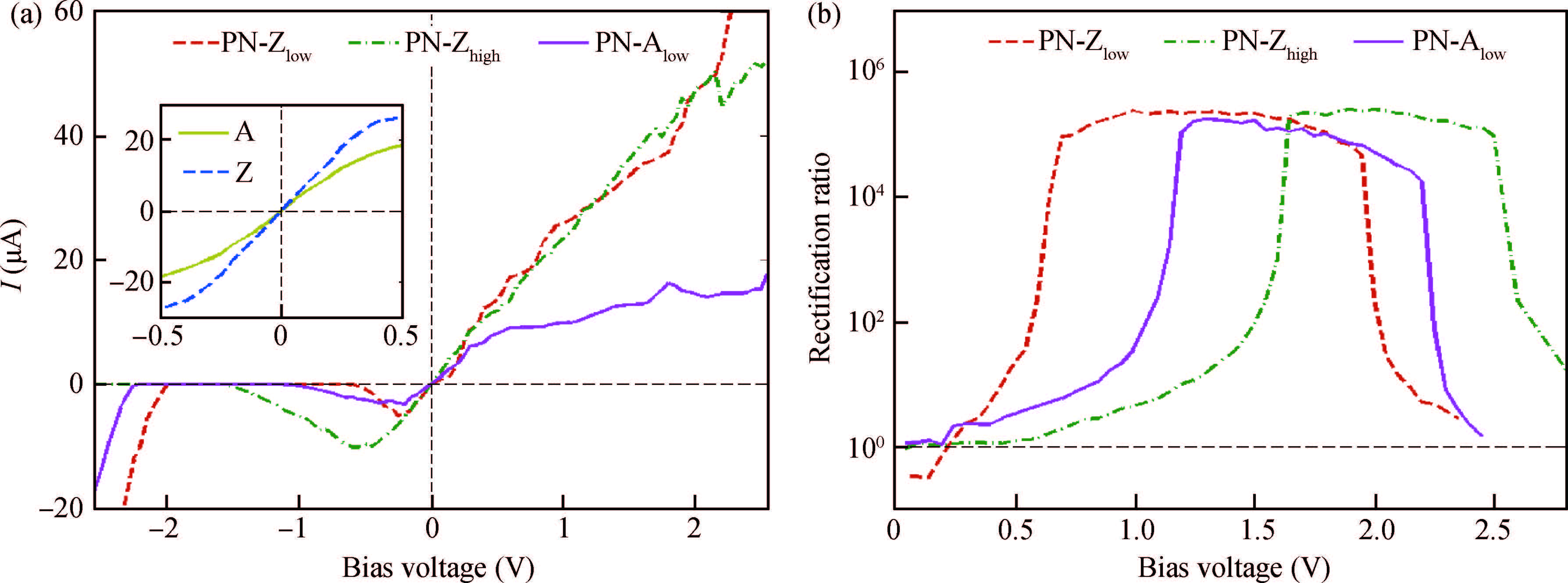
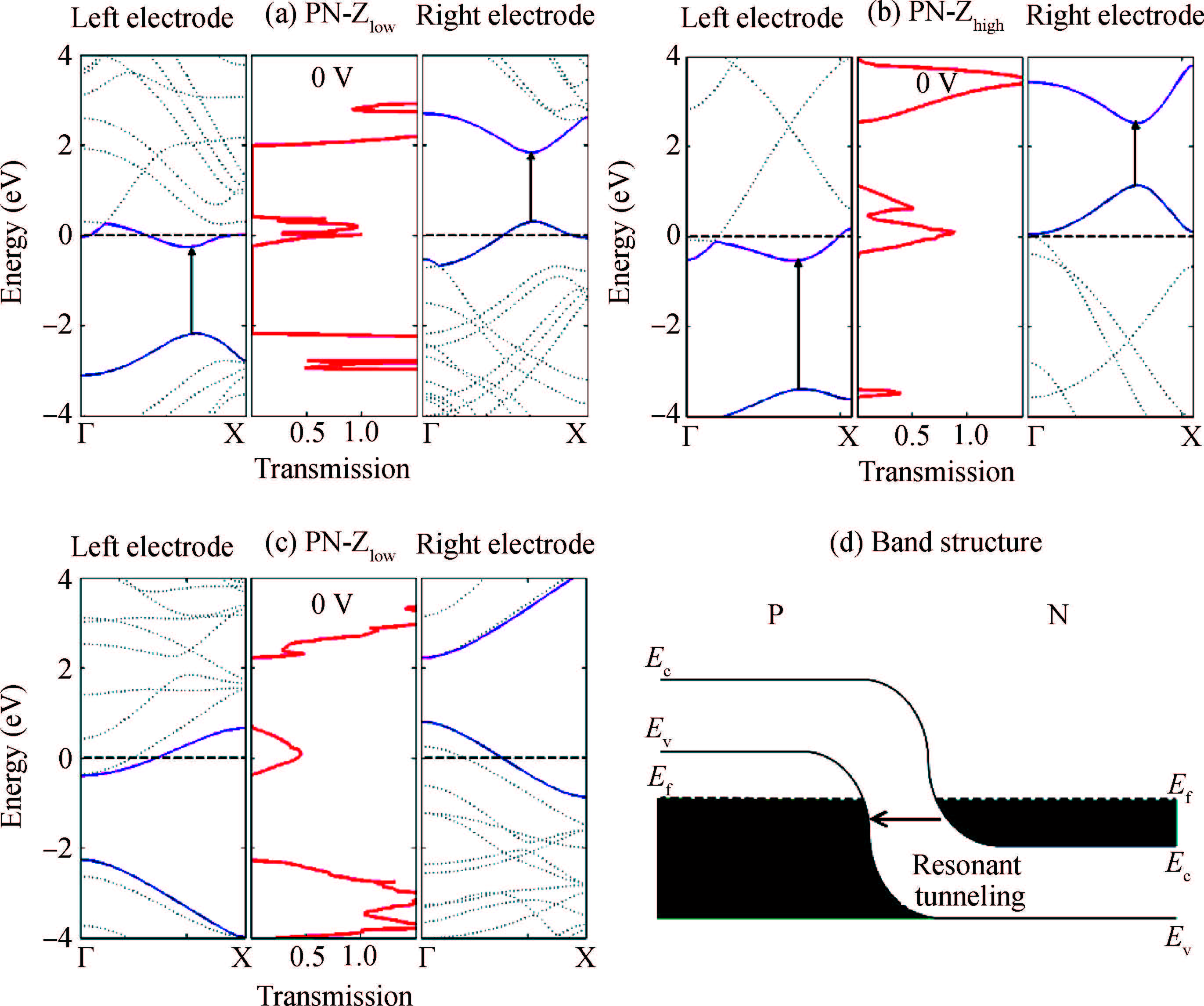
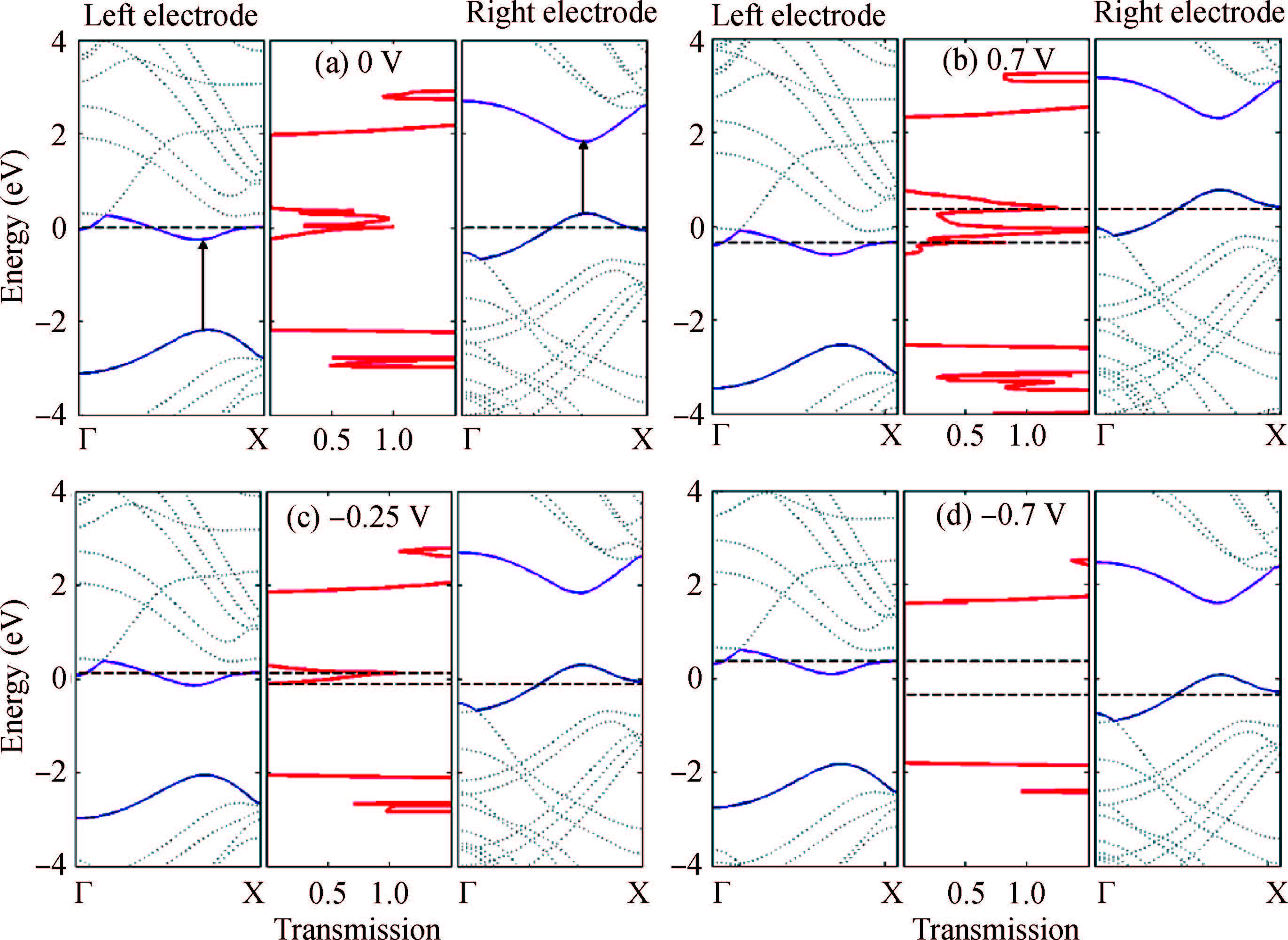
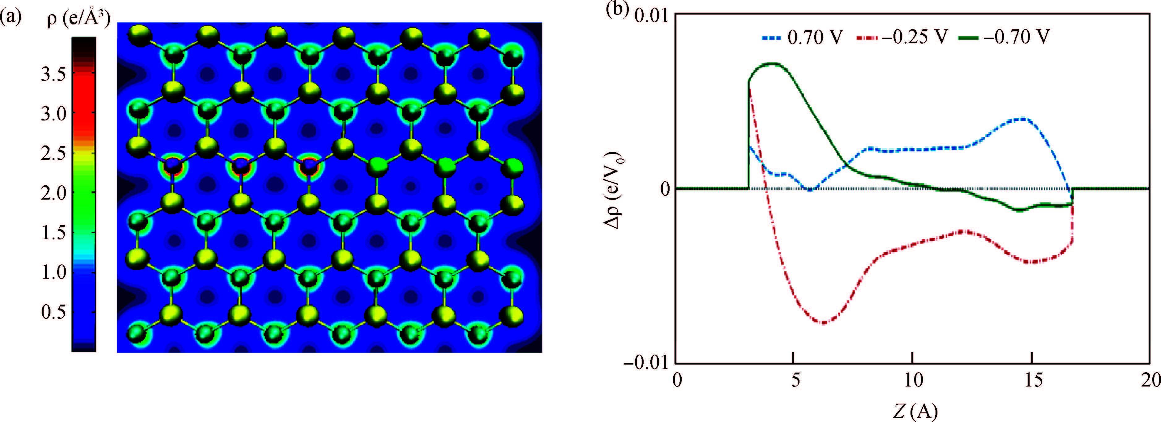
| [1] |
Bekaroglu E, Topsakal M, Cahangirov S, et al. First-principles studyofdefects andadatomsin siliconcarbide honeycombstructures. Phys Rev B, 2010, 81:075433 doi: 10.1103/PhysRevB.81.075433 |
| [2] |
Wu R, Zhou K, Yue C Y, et al. Recent progress in synthesis, properties and potential applications of SiC nanomaterials. Prog Mater Sci, 2015, 72:1 doi: 10.1016/j.pmatsci.2015.01.003 |
| [3] |
Li X W, Zhou J, Wang Q, et al. Magnetic properties of two dimensional silicon carbide triangular nanoflakes-based kagome lattices. Nanopart Res, 2012, 14:1056 doi: 10.1007/s11051-012-1056-5 |
| [4] |
Lin X, Lin S, Xu Y, et al. Ab initio study of electronic and optical behavior of two-dimensional silicon carbide. J Mater Chem C, 2013, 1:2131 doi: 10.1039/c3tc00629h |
| [5] |
Lou P J. Effects of edge hydrogenation in zigzag silicon carbide nanoribbons:stability,electronicandmagneticproperties,aswell as spin transport property. J Mater Chem C, 2013, 1:2996 doi: 10.1039/c3tc30173g |
| [6] |
Lin S S. Light-emitting two-dimensional ultrathin silicon carbide. J Phys Chem C, 2012, 116:3951 doi: 10.1021/jp210536m |
| [7] |
Ivanov P A, Chelnokov V E. Recent developments in SiC singlecrystal electronics. Semicond Sci Technol, 1992, 7:863 doi: 10.1088/0268-1242/7/7/001 |
| [8] |
Freeman C L, Claeyssens F, Allan N L. Graphitic nanofilms as precursors to wurtzite films:theory. Phys Rev Lett, 2006, 96:066102 doi: 10.1103/PhysRevLett.96.066102 |
| [9] |
Ding Y, Wang Y L. Density functional theory study of the silicene-like SiX and XSi 3(X D B, C, N, Al, P) honeycomb lattices:the various buckled structures and versatile electronic properties. J Phys Chem C, 2013, 117:18266 doi: 10.1021/jp407666m |
| [10] |
Mak K F, Lee C, Hone J, et al. Atomically thin MoS2:a new direct-gap semiconductor. Phys Rev Lett, 2010, 105:474
|
| [11] |
|
| [12] |
Sahin H, Cahangirov S, Topsakal M, et al. Monolayer honeycomb structures of group-IV elements and Ⅲ-V binary compounds:first-principles calculations. Phys Rev B, 2009, 80:155453 doi: 10.1103/PhysRevB.80.155453 |
| [13] |
|
| [14] |
Mitlehner H, Friedrichs P, Peters D, et al. Switching behavior of fast high voltage SiC pn-diodes. IEEE Proceedings of the 10th Int Symposium on Power Semiconductor Devices and ICs, 1998:127
|
| [15] |
Gupta J P, Andrainov A V, Kolodzey J, et al. Injection induced terahertz electroluminescence from 4H-SiC pn-junctions under forward bias. IEEE Infrared, Millimeter, and Terahertz Waves (IRMMW-THz), 38th Int. Conference, 2013:1
|
| [16] |
Novoselov K S, Geim A K, Morozov S V, et al. Two-dimensional gas of massless Dirac fermions in graphene. Nature, 2005, 438:197 doi: 10.1038/nature04233 |
| [17] |
Geim A K, Novoselov K S. The rise of graphene. Nat Mater, 2007, 6:183 doi: 10.1038/nmat1849 |
| [18] |
Mak K F, Sfeir M Y, Wu Y, et al. Measurement of the optical conductivity of graphene. Phys Rev Lett, 2008, 101:196405 doi: 10.1103/PhysRevLett.101.196405 |
| [19] |
Nair R R, Blake P, Grigorenko A N, et al. Fine structure constant defines visual transparency of graphene. Science, 2008, 320:1308 doi: 10.1126/science.1156965 |
| [20] |
Novoselov K S, Jiang D, Schedin F, et al. Two-dimensional atomic crystals. Proc Natl Acad Sci USA, 2005, 102:10451 doi: 10.1073/pnas.0502848102 |
| [21] |
Pacilé D, Meyer J C, Girit Ç Ö, et al. The two-dimensional phase of boron nitride:few-atomic-layer sheets and suspended membranes. Appl Phys Lett, 2008, 92:133107 doi: 10.1063/1.2903702 |
| [22] |
Meyer J C, Chuvilin A, Algara-Siller G J, et al. Selective sputtering and atomic resolution imaging of atomically thin boron nitride membranes. Nano Lett, 2009, 9:2683 doi: 10.1021/nl9011497 |
| [23] |
JinC,LinF,SuenagaK,etal. Fabricationofafreestandingboron nitride single layer and its defect assignments. Phys Rev Lett, 2009, 102:195505 doi: 10.1103/PhysRevLett.102.195505 |
| [24] |
Alem N, Erni R, Kisielowski C, et al. Atomically thin hexagonal boron nitride probed by ultrahigh-resolution transmission electron microscopy. Phys Rev B, 2009, 80:155425 doi: 10.1103/PhysRevB.80.155425 |
| [25] |
Fiori G. Negative differential resistance in mono and bilayer graphene pn junctions. IEEE Electron Device Lett, 2011, 32:1334 doi: 10.1109/LED.2011.2162392 |
| [26] |
Pospischil A, Furchi M M, Mueller T. Solar-energy conversion and light emission in an atomic monolayer p-n diode. Nat Nanotech, 2014, 9:257 doi: 10.1038/nnano.2014.14 |
| [27] |
Baugher B W H, Churchill H H, Yang Y, et al. Optoelectronic devices based on electrically tunable p-n diodes in a monolayer dichalcogenide. Nat Nanotech, 2014, 9:262 doi: 10.1038/nnano.2014.25 |
| [28] |
Ross J D, Klement P, Jones A M, et al. Electrically tunable excitonic light-emitting diodes based on monolayer WSe 2 p-n junctions. Nat Nanotech, 2014, 9:268 doi: 10.1038/nnano.2014.26 |
| [29] |
Kamiyama S, Maeda T, Nakamura Y, et al. Extremely high quantum efficiency of donor-acceptor-pair emission in N-and-Bdoped 6H-SiC. J Appl Phys, 2006, 99:093108 doi: 10.1063/1.2195883 |
| [30] |
Soler J M, Artacho E, Gale J D, et al. The SIESTA method for ab initio order-N materials simulation. J Phys Condens Matter, 2002, 14:2745 doi: 10.1088/0953-8984/14/11/302 |
| [31] |
Brandbyge M, Mozos J L, Ordejon P. Density-functional method for nonequilibrium electron transport. Phys Rev B, 2002, 65:165401 doi: 10.1103/PhysRevB.65.165401 |
| [32] |
Soler J M, Artacho E, Gale J D, et al. The SIESTA method for ab initio order-N materials simulation. J Phys Condens Matter, 2002, 14:2745 doi: 10.1088/0953-8984/14/11/302 |
| [33] |
Zhang D H, Yo K L, Gao G Y. The peculiar transport properties in p-n junctions of doped graphene nanoribbons. J Appl Phys, 2011, 110:013718 doi: 10.1063/1.3605489 |
| [34] |
|
| [35] |
Perrin M L, Galan E, Eelkema R. Single-molecule resonant tunneling diode. J Phys Chem C, 2015, 119:5697 doi: 10.1021/jp512803s |
| [36] |
Liu F, Wang J, Guo H. Negative differential resistance in monolayer WTe 2 tunneling transistors. Nanotechnology, 2015, 26:175201 doi: 10.1088/0957-4484/26/17/175201 |
| [37] |
Li J, Guo H, Liu J, et al. GaAs-based resonant tunneling diode (RTD) epitaxy on Si for highly sensitive strain gauge applications. Nanoscale Res Lett, 2013, 8:218 doi: 10.1186/1556-276X-8-218 |
| [38] |
|
| [39] |
Son N T, Chen W M, Kordina O, et al. Electron effective masses in 4H SiC. Appl Phys Lett, 1995, 66:1074 doi: 10.1063/1.113576 |


 DownLoad: