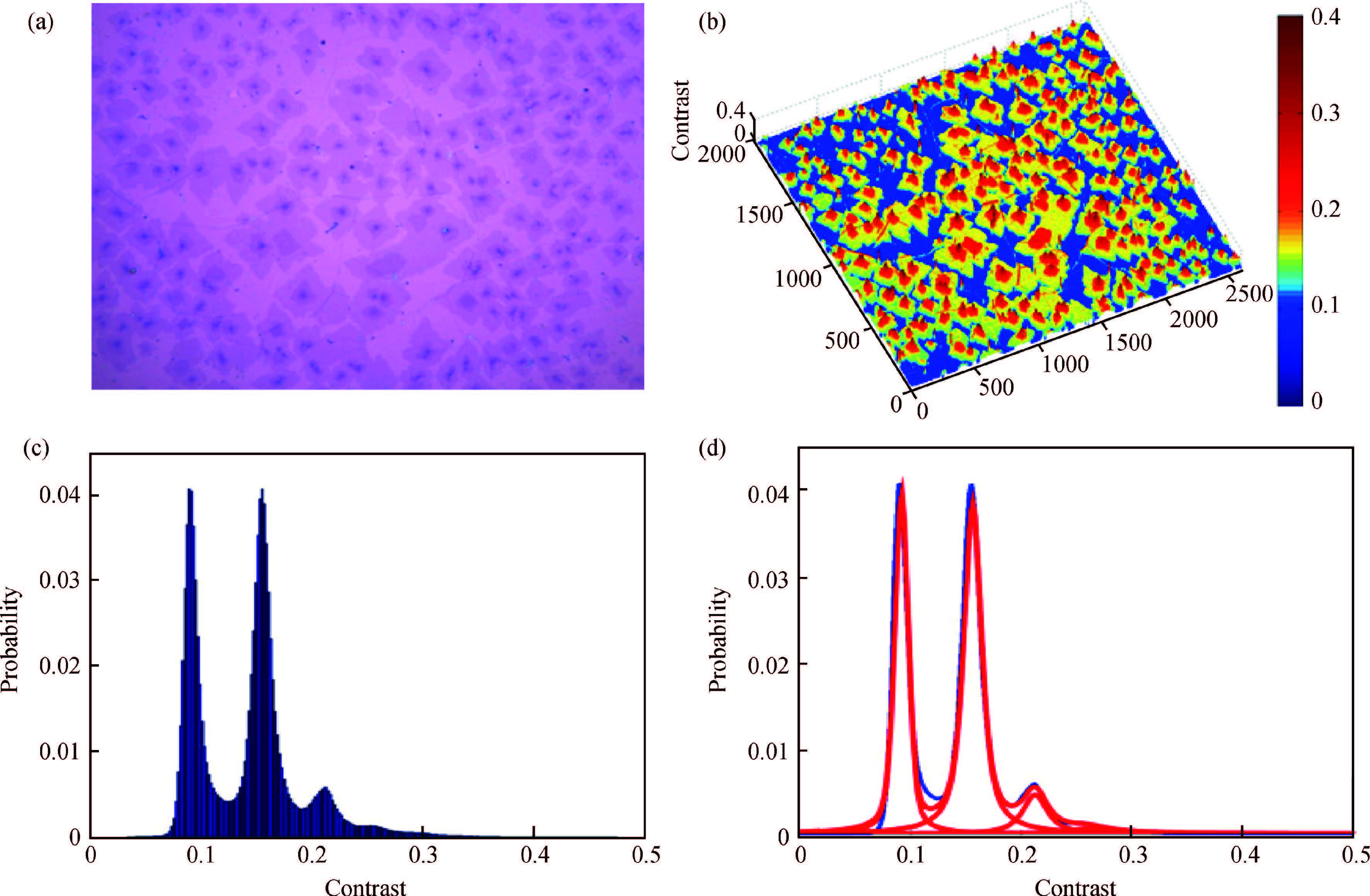
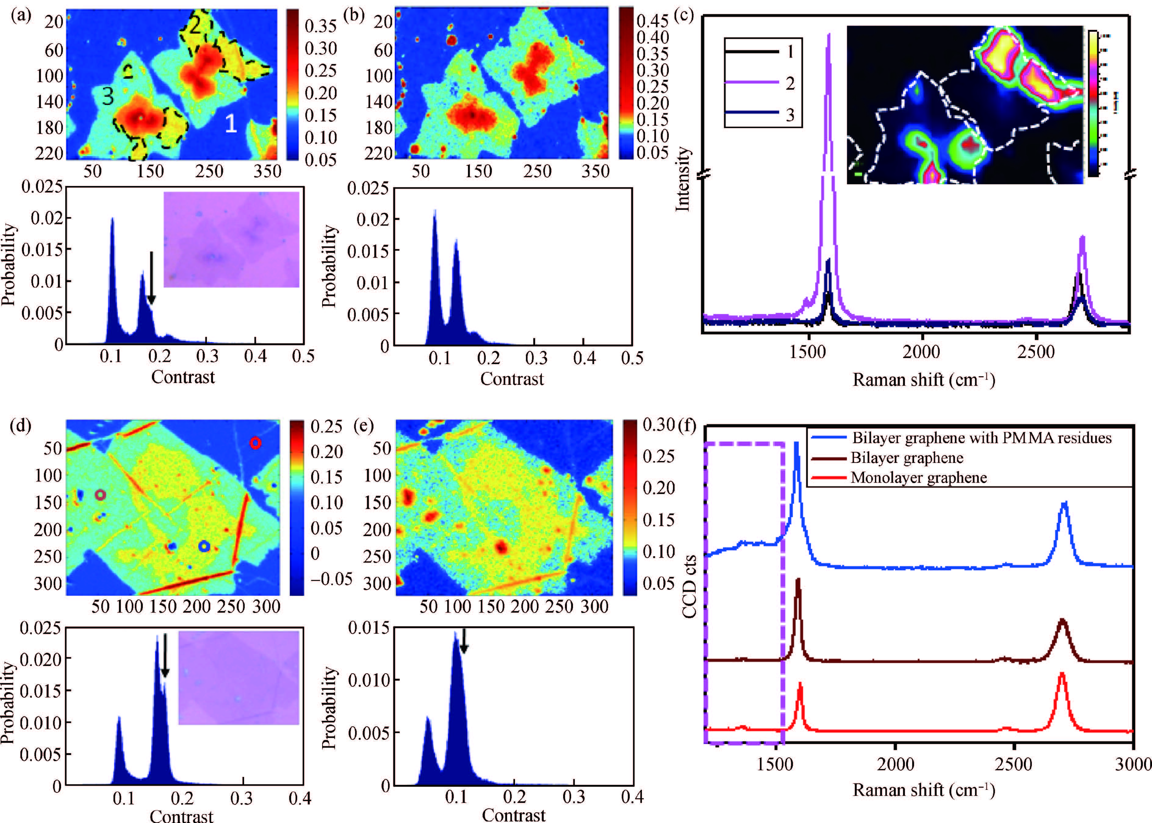
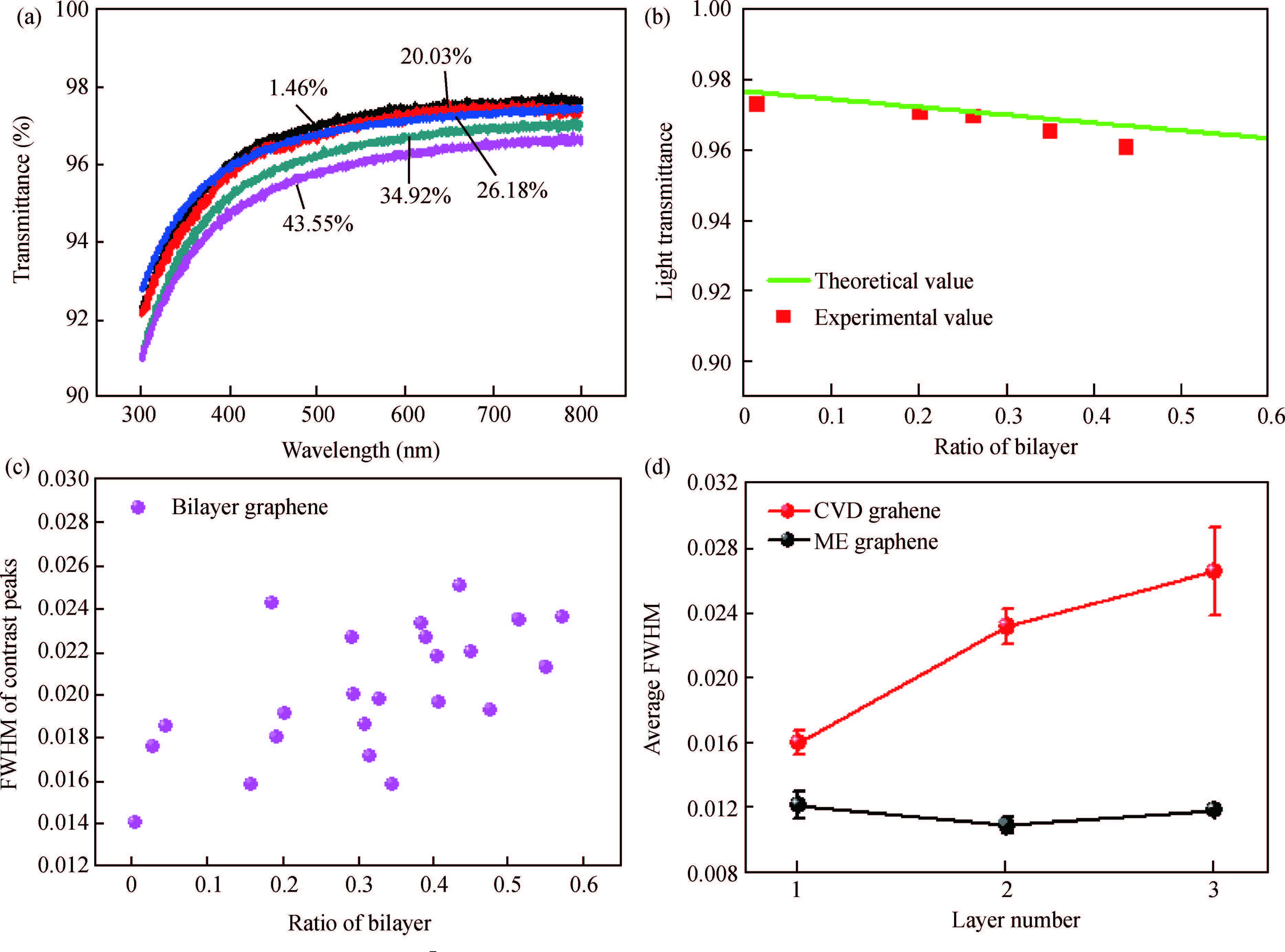
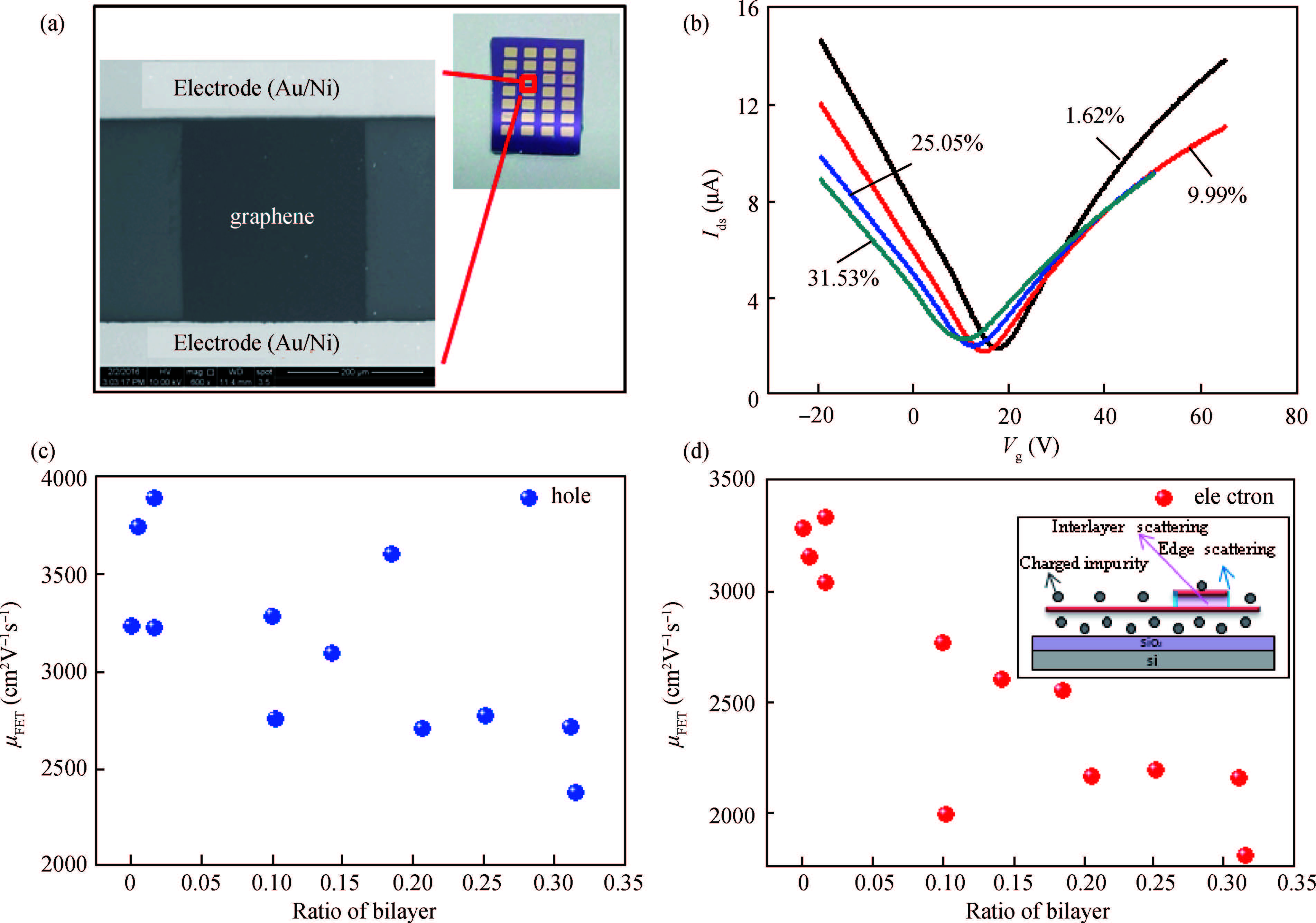
1. Introduction
Large area graphene grown by the chemical vapor deposition (CVD) method is the most promising route to realizing mass production and commercialization of electronics[1]. However, multi-layer domains always appear at the nucleation centers during CVD growth[2]. The emergence of multi-layer domains will increase carrier scattering at the edge of grains and also affect the light transmittance. Besides, the electronic band structures of graphene will also be altered with the change of twist angles between graphene layers[3], which lead to the changes of a series of properties, for instance, Van Hove singularities [4, 5], optical conductivity[6] and Raman features[7-10]. Therefore, the systematical investigation of the properties of large-scale graphene with multi-layer domains is important both for fundamental researches and industrial applications.
Raman spectroscopy[7-10], transmission electron microscopy (TEM)[11, 12], and scanning tunneling microscopy (STM)[13] have been widely used to study the properties of bi-/multi-layer graphene domains, however these techniques are time consuming and with low throughput. On the other side, optical contrast and imaging are utilized as effective and non-destructive methods to obtain information on graphene and other two-dimensional materials, including thickness and layer numbers, absorptions, and inter-layer interactions[6, 14-18].
In this study, large-scale CVD monolayer graphene covered by multi-layer domains were systematically investigated by optical imaging. We propose that optical imaging with light illumination correction can be used to obtain the coverage of mono- and multi-layer domains in large-scale CVD graphene effectively and accurately. More importantly, the twist angles between graphene layers and the impurities absorbed on the surface of graphene could also be probed by optical contrast and imaging. Finally, field effect mobility of CVD graphene with different bilayer coverage was investigated, where the bilayer domains behave as scattering sources and seriously limit the mobility of graphene.
2. Results and discussions
2.1 Large-scale thickness identification by optical imaging
We firstly propose a method for large-scale thickness identification of graphene layers using optical imaging, which can also be used to analyze the coverage of mono- and multi-layer domains. The optical image of mono- and multi-layer mechanically exfoliated graphene on SiO2(285 nm)/Si substrate is shown in Fig. 1(a). The Green (G)-channel optical contrast values at each pixel can be calculated from the image using the equation below[18]:

C=Gsub−GsamGsub, |
where Gsam and Gsub are the G-channel values taken from the optical images of the graphene sample and the substrate by Matlab software, respectively. During the analysis, it was found that the light illumination under a microscope is non-uniform, which is clearly demonstrated by the clean substrate in Fig. 1(b). Therefore, the optical contrast image obtained by taking a constant value of Gsub is not uniform even for graphene sheets with the same thickness (Fig. 1(c)). Such an effect would be even more significant for large-scale thickness identification, i.e. in the case of large-scale CVD graphene. Therefore, the light illumination correction has been considered during the image processing procedure. An optical image of a clean substrate was taken under the same illumination and used as background for obtaining Gsub at each pixel (Fig. 1(b)[14]. Fig. 1(d) is the three-dimensional (3D) optical contrast image with light illumination correction. Compared with Fig. 1(c), we can clearly find that the correction method effectively eliminates the influence of non-uniform light illumination and makes graphene layers with different thicknesses highly distinguishable.
Using this technique we then analyze the large-scale CVD grown monolayer graphene samples with multilayer domains. The optical image and the 3D image of G value contrast are shown in Figs. 2(a) and 2(b), respectively. For comparison, the optical contrast imaging of the same sample without light illumination correction is shown in Fig. S1 (Supplementary information). The thicknesses of graphene layers are confirmed by Raman spectrum and imaging[19, 20], as shown in Fig. S2. We can then obtain the statistical distribution of G contrast values at each pixel in the whole optical image using Matlab software, as shown in Fig. 2(c). There are mainly four distinguishable contrast peaks in the histogram curve, which correspond to the contrasts of CVD graphene with 1-4 layers. By curve fitting, we can then obtain the center position and also the area of each peak.
Table 1 gives the fitting results. The center positions of each peak are very close to the theoretical G-channel contrast values of 1-4 layer Bernal-stacked graphene layers (0.077 for 1 layer, 0.149 for 2 layers, 0.216 for 3 layers, 0.278 for 4 layers)[18]. The ratio of coverage for graphene domains with different thicknesses can then be calculated from the area of each contrast peak in Fig. 2(d). For the sample shown in Fig. 2(a), the coverage of monolayer to four-layer graphene is 36.46%, 52.42%, 9.01%, and 2.11%, respectively. Therefore, the contrast imaging analysis provides a simple, non-destructive and practical way for quick identification of graphene layer numbers and also the coverage of multilayer domains in large-scale. This approach is better performed in the thickness analysis of mechanically exfoliated graphene, which has a much narrower full width at half maximum (FWHM) of the contrast peak in the histogram curve due to the uniformity and cleanness of the sample, as shown in Fig. S3.
Parameter | Peak position | Layer-ratio |
Monolayer | 0.091 | 36.46% |
Bilayer | 0.155 | 52.42% |
Trilayer | 0.211 | 9.01% |
Four-layer | 0.259 | 2.11% |
In the following, we will discuss the two factors that could affect the optical contrast of bi-/multi-layer graphene domains. In the optical contrast image of Fig. 3(a), we found that some bilayer regions have slight higher contrast as compared to others, as shown by the yellow colors. The yellow color regions actually correspond to the shoulder peak near the contrast peak of the bilayer, as labeled by the black arrow. From Raman spectra and Raman imaging of the G peak intensity, it can be clearly seen that the yellow color regions are twisted bilayer graphene (TBG) with G peak resonance (with a tens of times stronger G peak intensity as compared to monolayer graphene), as displayed in Fig. 3(c). It is reported that the joint density of states (JDOS) and the optical transition matrix element (Mop) for parallel band transitions lead to the enhancement of Raman G peak intensity and light absorption for a laser with similar excitation energies[8]. For our excitation laser with energy of 2.41 eV (514 nm), the G peak resonance happens for TBG with a twist angle of approximately 13°[21]. Since the enhancement of optical absorption by 13° TBG locates within the G-channel wavelength region, it would not affect the R-channel optical contrast. This is clearly demonstrated in Fig. 3(b), where the TBG region with G peak resonance is not distinguishable from other bilayer domains. It should be noted that TBG with other twist angles will also introduce additional absorption at a different light wavelength, which would change the optical contrast values. This is one of the reasons why the FWHM of contrast peaks for multi-layer graphene in the histogram curve is much wider than that of monolayer graphene in Fig. 2(d) (also Fig. 4(d) in the later section).


In addition to the twist angle of graphene layers, the impurities that are absorbed on the graphene surface would also affect the optical contrast of graphene, e.g. poly(methyl methacrylate) (PMMA) residues during the transfer process of CVD graphene. The graphene sample shown in Fig. 3(d) was transferred with a standard PMMA transfer procedure[22] and annealed at 300 ℃ in atmosphere for 30 min to remove PMMA. In this case, there would be PMMA residue on the graphene surface unavoidably. Other samples mentioned in our paper were all transferred by PMMA but removed by acetone to minimize the PMMA residue. The optical contrast images shown in Figs. 3(d) and 3(e) clearly reveal some yellow color regions with contrast values higher than other bilayer regions. Raman spectra shown in Fig. 3(f) confirm that the yellow area regions are actually graphene with PMMA residues[23]. Annealing at 300 ℃ in air leads to the disintegration of PMMA macromolecules, with various lengths of disintegrated fragments corresponding to the broad Raman peaks at 1050-1550 cm-1 in the blue curve in Fig. 3(f)[23, 24]. Some fragment may also form covalent bonds with graphene at the defect location and changes the optical absorption[25]. The PMMA residues would change both the G and R channel optical contrast of graphene, which is different from the case of TBG domains as discussed above. It should be noted that the change of optical contrast from the above two situations is not significant, which appear only as a shoulder peak aside to the bilayer one in the histogram curve. As a result, they would not greatly affect the thickness and coverage analysis of multilayer graphene.
2.2 The effect of bilayer domains on the optical properties of CVD graphene
We then focus on the effect of bilayer domains on the optical properties of CVD monolayer graphene. The same batch of CVD graphene samples were transferred to SiO2(285 nm)/Si substrate and quartz plate for optical contrast and transmittance measurements, respectively. The coverage of bilayer domains were obtained through contrast measurement as discussed in Section 2.1. Fig. 4(a) displays the transmittance spectra of CVD graphene samples with different bilayer coverage, i.e. 1.46%, 20.03%, 26.18%, 34.92%, and 43.55%, respectively. As can be seen, with the increase of bilayer coverage, the transmittance of CVD graphene decreases gradually. Fig. 4(b) shows the relation between light transmittance at 550 nm and bilayer coverage. It is obvious that light transmittance monotonically decreases with the increase of bilayer coverage. The absorption of monolayer and Bernal-stacked bilayer graphene in the visible range is approximately 2.3% and 4.6%, respectively[26]. However, we found that there is a deviation from the theoretical values for CVD graphene with a larger coverage of bilayer domains. This could be explained by the extra light absorption caused by parallel bands transition of TBG[8]. Fig. 4(c) shows the dependence of the FWHM of the optical contrast peak on the bilayer coverage, which suggests that the possibility of the stacking disorders with various angles increases with the increase of bilayer coverage. Since various twist angles of TBG correspond to the alteration of van Hove singularities in the DOS[6] and hence different resonant absorption wavelength, it will then contribute to the extra light absorption CVD graphene with larger coverage of bilayer domains. We further compare the FWHM of contrast peaks of exfoliated graphene and CVD graphene with different thicknesses. As shown in Fig. 4(d), for CVD graphene samples, the average FWHM of peaks increases monotonically with the increase of layer number, while this value is almost unchanged for multilayer exfoliated graphene with Bernal-stacking geometry.
2.3 The effect of bilayer domains on the electrical properties of CVD graphene
The mobility of graphene is a very important parameter for electrical and optoelectronic applications[27]. Since multi-layer domains are easily formed in CVD graphene, it is meaningful to investigate the relationship between carrier mobility and the coverage of multi-layer domains. Monolayer graphene samples with uniformly distributed bilayer domains on SiO2(285 nm)/Si substrate were patterned by using UV lithography and O2 plasma etching [shown in Fig. 5(a), with size of ~ 290 μm (length) × ~ 270 μm (width)], and the metal contact [Ni (5 nm)/Au (50 nm)] was then thermally evaporated. Next, we characterized the transfer characteristics of these back-gate graphene field-effect devices at an applied bias voltage of Vds= 0.01 V. Fig. 5(b) depicts the transfer characteristics of monolayer graphene with different bilayer coverage. The optical images and their G-channel contrast distributions of the samples are shown in Fig. S4 (Supplementary information). The Dirac point is located in the positive gate voltage region, which indicates that these devices are lightly p-doped due to a small amount of PMMA residue or other charged impurities on the above[28]. With the increase of bilayer coverage, the slope of the curves gradually decreases. The highest field-effect carrier mobility μ of the devices is extracted according to the equation below:

μ=gmLWVdsCg, |
where
As shown in Figs. 5(c) and 5(d), it is obvious that the hole and electron mobility monotonically decrease with the increase of bilayer coverage. The hole mobility decreases from ~ 3900 to ~ 2400 cm2V-1s-1, while the electron mobility decreases from ~ 3300 to ~ 1800 cm2V-1s-1, with ~ 30% bilayer coverage. This trend can be explained by additional scattering sources and band structure alteration with bilayer domains, as schematically illustrated in the inset of Fig. 5(d). The major scattering sources of graphene should be remote Coulomb scattering coming from charged impurities at the top and bottom surfaces and interlayer scattering at bilayer domains[29]. Compared to monolayer, the carrier mobility of bilayer graphene is lower due to extra interlayer scattering[30]. Moreover, because of the existence of built-in potential at the single and bilayer boundary, charges would accumulate, and the mobility of carriers might be limited by Coulomb scattering when they drift across these regions. The above results do reveal that a few bilayer domains could significantly affect the electrical performance of monolayer graphene, and hence its application in electronics and optoelectronics.
3. Conclusions
In summary, we propose an optical imaging technique with light illumination corrected optical contrast to accurately identify the thickness and coverage of multi-layer domains in large-scale CVD grown monolayer graphene. It is also demonstrated that the twist angles of TBG and the impurities absorbed on the surface of graphene could be probed by the optical contrast and imaging. From the investigation of the effects of bilayer domains, we found that the carrier mobility of CVD graphene is obviously limited by the scattering from bilayer domains. Our results could be significant for guiding the future optoelectronic applications of large-scale CVD graphene. In addition, the optical imaging technique also provides an effective way to study the properties of other two-dimensional materials.