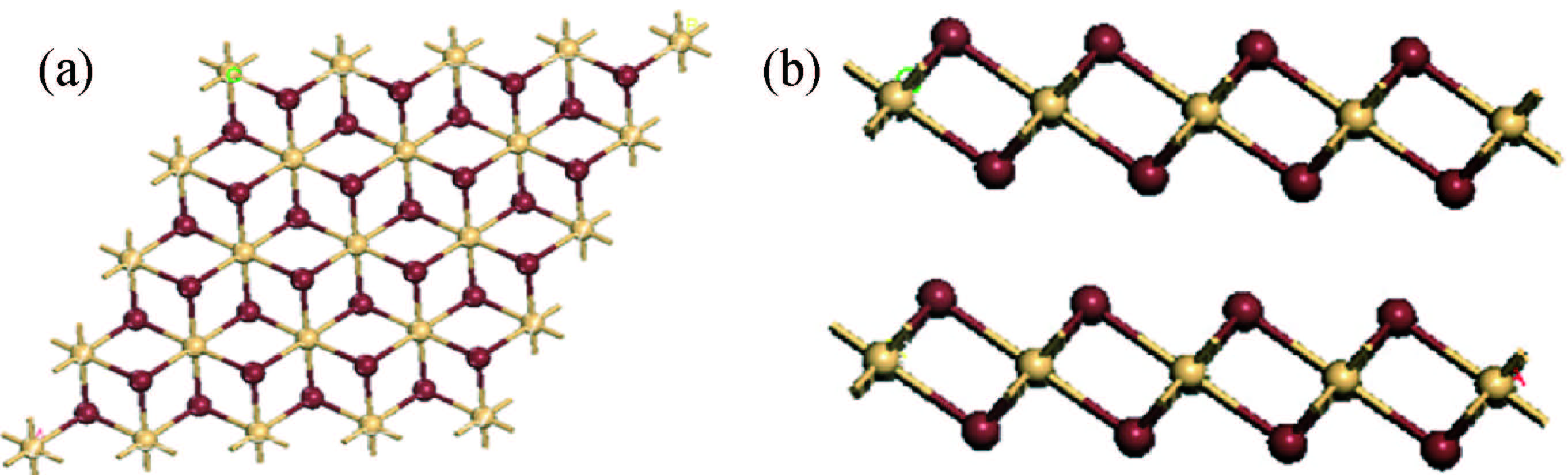
Fig. 1.
(Color online) Top and side view of geometric structures of ZrS2 bilayer.
SPECIAL TOPIC ON 2D MATERIALS AND DEVICES
Jimin Shang, Le Huang and Zhongming Wei
Corresponding author: Jimin Shang,Email:sjm@zzuli.edu.cn
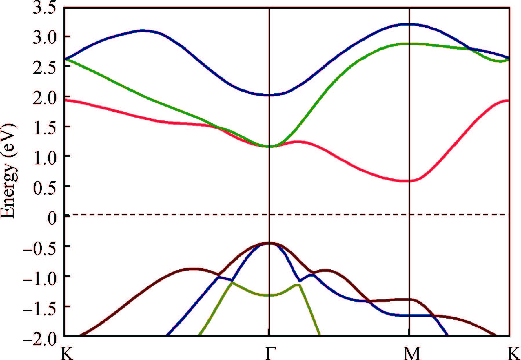
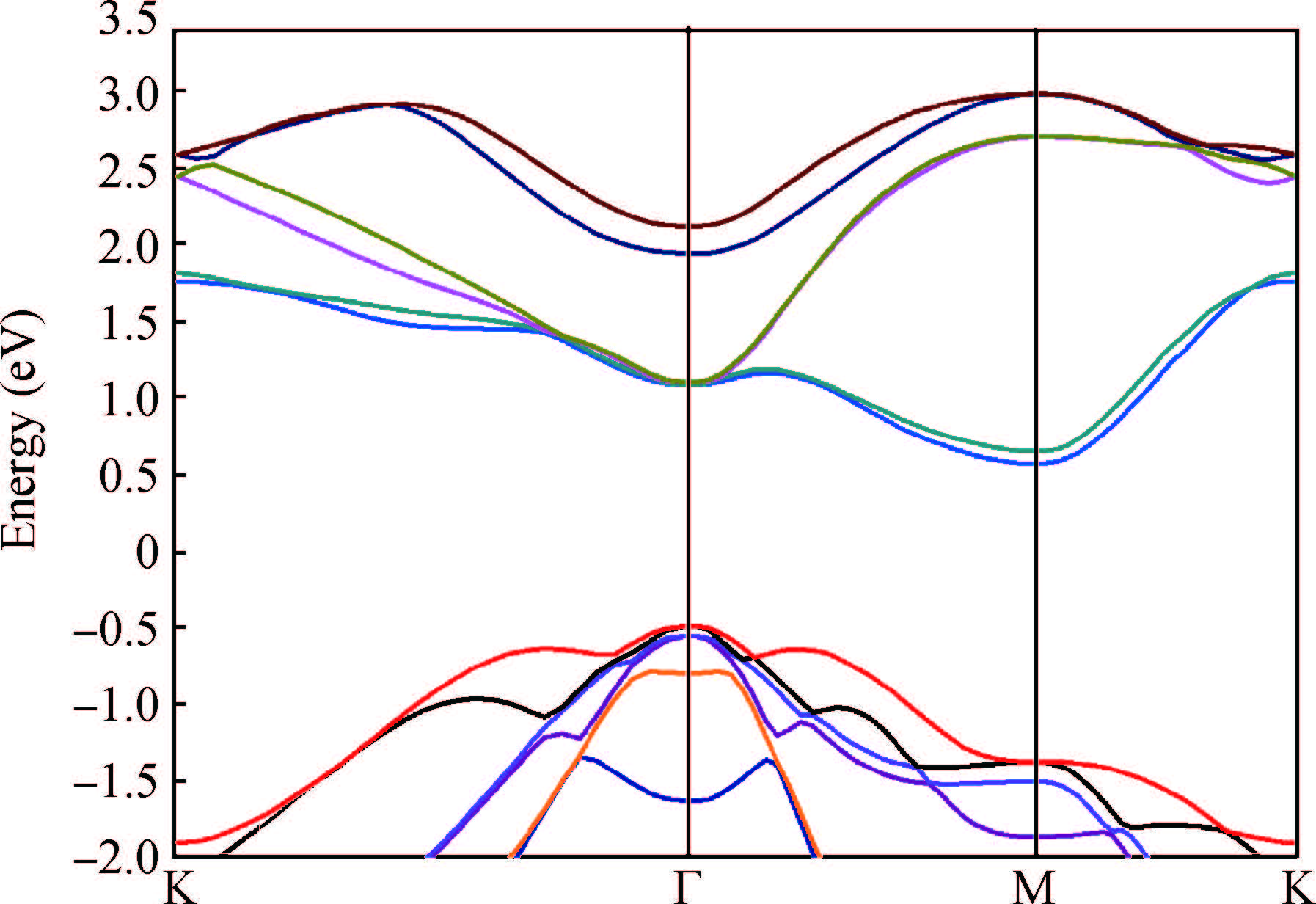
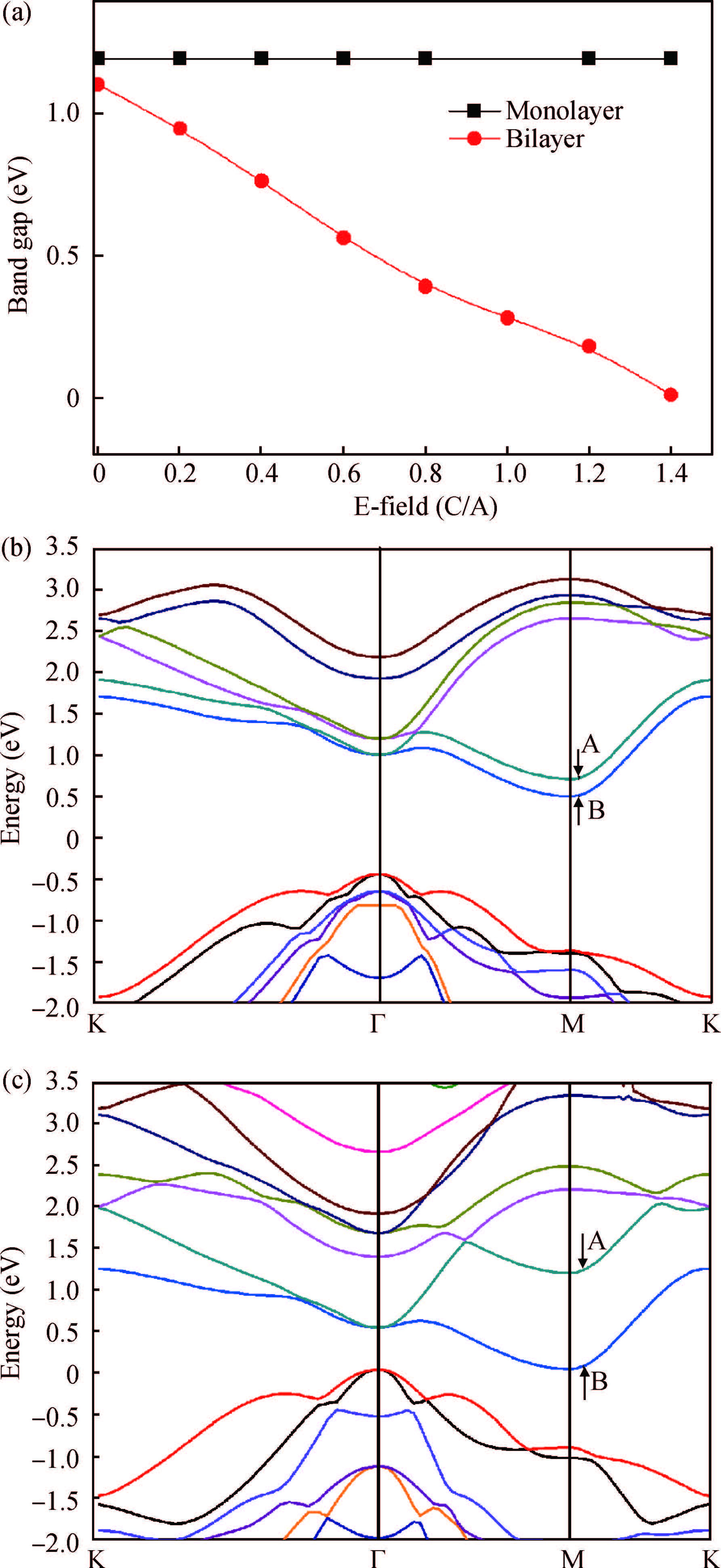
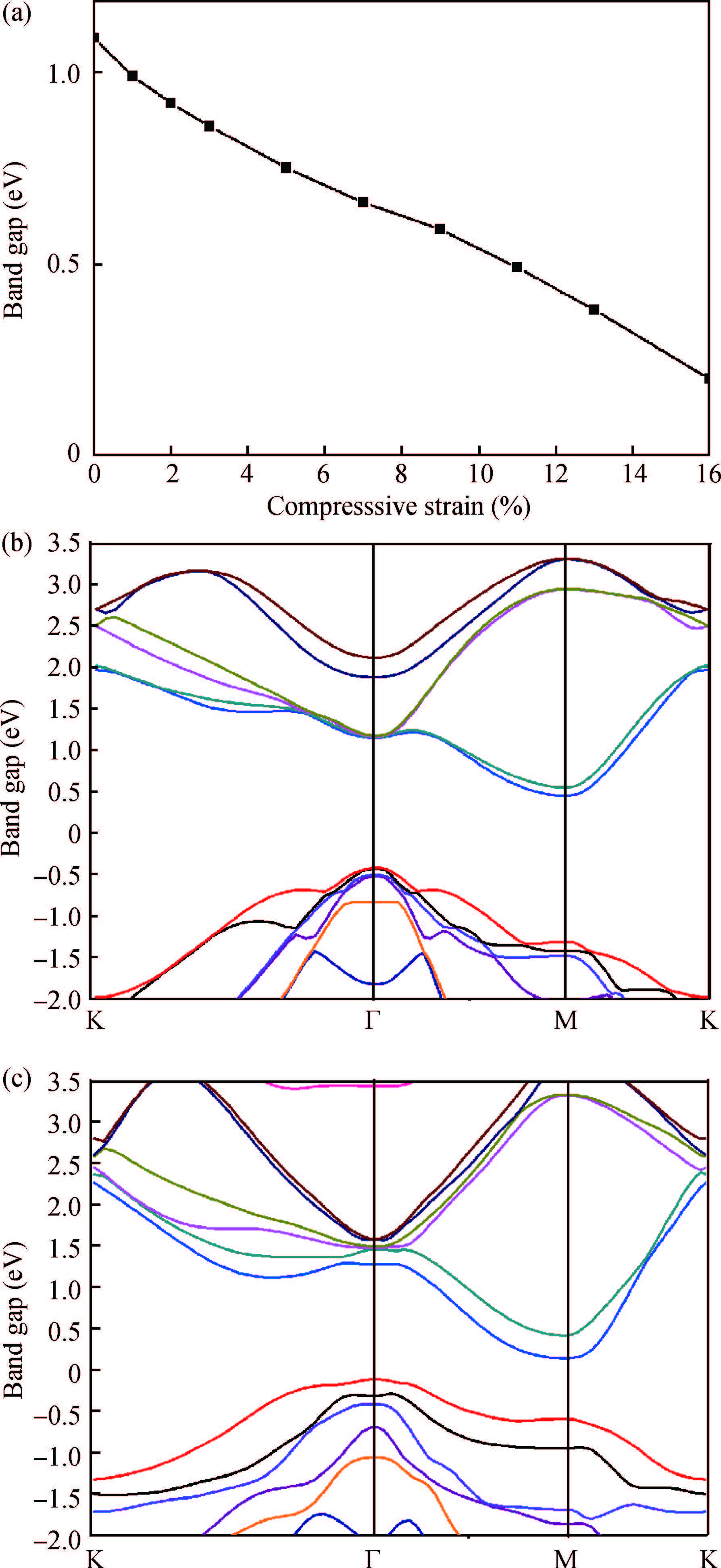
Abstract: Using first-principles calculations, including Grimme D2 method for van der Waals interactions, we investigate the tuning electronic properties of bilayer zirconium disulfides (ZrS2) subjected to vertical electric field and normal compressive strain. The band gap of ZrS2 bilayer can be flexibly tuned by vertical external electric field. Due to the Stark effect, at critical electric fields about 1.4 V/Å, semiconducting-metallic transition presents. In addition, our results also demonstrated that the compressive strain has an important impact on the electronic properties of ZrS2 bilayer sheet. The widely tunable band gaps confirm possibilities for its applications in electronics and optoelectronics.
Keywords: vertical electric field, normal compressive strain, electronic properties, zirconium disulfides bilayer
| [1] |
Li Y, Tongay S, Yue Q, et al. Metal to semiconductor transition in metallic transition metal dichalcogenides. J Appl Phys, 2013, 114(17):174307 doi: 10.1063/1.4829464
|
| [2] |
Mak K F, Lee C, Hone J, et al. Atomically thin MoS2:a new direct-gap semiconductor. Phys Rev Lett, 2010, 105(24):136805
|
| [3] |
Splendiani A, Sun L, Zhang Y, et al. Emerging photoluminescence in monolayer MoS2. Nano Lett, 2010, 10(4):1271 doi: 10.1021/nl903868w
|
| [4] |
Wang Q H, Kalantar-Zadeh K, Kis A, et al. Electronics and optoelectronics of two-dimensional transition metal dichalcogenides. Nat Nanotechnol, 2012, 7(11):699 doi: 10.1038/nnano.2012.193
|
| [5] |
Kuc A, Zibouche N, Heine T. Influence of quantum confinement on the electronic structure of the transition metal sulfide TS2. Phys Rev B, 2011, 83(24):245213 doi: 10.1103/PhysRevB.83.245213
|
| [6] |
Li Y, Yang S, Li J. Modulation of the electronic properties of ultrathin black phosphorus by strain and electrical field. J Phys Chem C, 2014, 118(41):23970 doi: 10.1021/jp506881v
|
| [7] |
Kumar A, Ahluwalia P K. Mechanical strain dependent electronic and dielectric properties of two-dimensional honeycomb structures of MoX2(X D S, Se, Te). Physica B, 2013, 419:66 doi: 10.1016/j.physb.2013.03.029
|
| [8] |
Zeng Z, Yin Z, Huang X, et al. Single-layer semiconducting nanosheets:high-yield preparation and device fabrication. Angewandte Chemie Int Ed, 2011, 50(47):11093 doi: 10.1002/anie.v50.47
|
| [9] |
Li L, Fang X, Zhai T, et al. Electrical transport and highperformance photoconductivity in individual ZrS2 nanobelts. Adv Maters, 2010, 22(37):4151 doi: 10.1002/adma.v22:37
|
| [10] |
Li L, Wang H, Fang X, et al. High-performance Schottky solar cells using ZrS2 nanobelt networks. Energy Environ Sci, 2011, 4(7):2586 doi: 10.1039/c1ee01286j
|
| [11] |
Li Y, Kang J, Li J. Indirect-to-direct band gap transition of the ZrS2 monolayer by strain:first-principles calculations. RSC Adv, 2014, 4(15):7396 doi: 10.1039/c3ra46090h
|
| [12] |
Yu E K, Stewart D A, Tiwari S. Ab initio study of polarizability and induced charge densities in multilayer graphene films. Phys Rev B, 2008, 77(19):195406 doi: 10.1103/PhysRevB.77.195406
|
| [13] |
McCann E. Asymmetry gap in the electronic band structure of bilayer graphene. Phys Rev B, 2006, 74(16):161403 doi: 10.1103/PhysRevB.74.161403
|
| [14] |
Liu Q, Li L, Li Y, et al. Tuning electronic structure of bilayer MoS2 by vertical electric field:a first-principles investigation. J Phys Chem C, 2012, 116(40):21556 doi: 10.1021/jp307124d
|
| [15] |
Qi J, Li X, Qian X, et al. Bandgap engineering of rippled MoS2 monolayer under external electric field. Appl Phys Lett, 2013, 102(17):173112 doi: 10.1063/1.4803803
|
| [16] |
Manjanath A, Samanta A, Pandey T, et al. Semiconductor to metal transition in bilayer phosphorene under normal compressive strain. Nanotechnology, 2015, 26(7):075701 doi: 10.1088/0957-4484/26/7/075701
|
| [17] |
Huang L, Li Y, Wei Z, et al. Strain induced piezoelectric effect in black phosphorus and MoS2 van der Waals heterostructure. Sci Rep, 2015, 5:16448 doi: 10.1038/srep16448
|
| [18] |
Kresse G, Furthmüller J. Efficiency of ab-initio total energy calculations for metals and semiconductors using a plane-wave basis set. Comput Mater, 1996, 6(1):15 doi: 10.1016/0927-0256(96)00008-0
|
| [19] |
Grimme S. Semiempirical GGA-type density functional constructed with a long-range dispersion correction. J Comput Chem, 2006, 27(15):1787 doi: 10.1002/(ISSN)1096-987X
|
| [20] |
Zywietz T, Neugebauer J, Scheffler M. Adatom diffusion at GaN (0001) and (0001) surfaces. Appl Phys Lett, 1998, 73(4):487 doi: 10.1063/1.121909
|
| [21] |
Ramasubramaniam A, Naveh D, Towe E. Tunable band gaps in bilayer transition-metal dichalcogenides. Phys Rev B, 2011, 84(20):205325 doi: 10.1103/PhysRevB.84.205325
|
| [22] |
Wu S, Ross J S, Liu G B, et al. Electrical tuning of valley magnetic moment through symmetry control in bilayer MoS2. Nat Phys, 2013, 9(3):149 doi: 10.1038/nphys2524
|
| [23] |
Jiang H. Structural and electronic properties of ZrX2 and HfX2(X D S and Se) from first principles calculations. J Chem Phys, 2011, 134(20):204705 doi: 10.1063/1.3594205
|
| [24] |
Greenaway D L, Nitsche R. Preparation and optical properties of group IV-VI2 chalcogenides having the CdI2 structure. J Phys Chem Solids, 1965, 26(9):1445 doi: 10.1016/0022-3697(65)90043-0
|
| [25] |
Guo H, Lu N, Dai J, et al. Phosphorene nanoribbons, phosphorus nanotubes, and van der Waals multilayers. J Phys Chem C, 2014, 118(25):14051 doi: 10.1021/jp505257g
|


Article views: 5610 Times PDF downloads: 68 Times Cited by: 0 Times
Received: 15 August 2016 Revised: 24 November 2016 Online: Published: 01 March 2017
| Citation: |
Jimin Shang, Le Huang, Zhongming Wei. Effects of vertical electric field and compressive strain on electronic properties of bilayer ZrS2[J]. Journal of Semiconductors, 2017, 38(3): 033001. doi: 10.1088/1674-4926/38/3/033001
****
J M Shang, L Huang, Z M Wei. Effects of vertical electric field and compressive strain on electronic properties of bilayer ZrS2[J]. J. Semicond., 2017, 38(3): 033001. doi: 10.1088/1674-4926/38/3/033001.

|
| [1] |
Li Y, Tongay S, Yue Q, et al. Metal to semiconductor transition in metallic transition metal dichalcogenides. J Appl Phys, 2013, 114(17):174307 doi: 10.1063/1.4829464
|
| [2] |
Mak K F, Lee C, Hone J, et al. Atomically thin MoS2:a new direct-gap semiconductor. Phys Rev Lett, 2010, 105(24):136805
|
| [3] |
Splendiani A, Sun L, Zhang Y, et al. Emerging photoluminescence in monolayer MoS2. Nano Lett, 2010, 10(4):1271 doi: 10.1021/nl903868w
|
| [4] |
Wang Q H, Kalantar-Zadeh K, Kis A, et al. Electronics and optoelectronics of two-dimensional transition metal dichalcogenides. Nat Nanotechnol, 2012, 7(11):699 doi: 10.1038/nnano.2012.193
|
| [5] |
Kuc A, Zibouche N, Heine T. Influence of quantum confinement on the electronic structure of the transition metal sulfide TS2. Phys Rev B, 2011, 83(24):245213 doi: 10.1103/PhysRevB.83.245213
|
| [6] |
Li Y, Yang S, Li J. Modulation of the electronic properties of ultrathin black phosphorus by strain and electrical field. J Phys Chem C, 2014, 118(41):23970 doi: 10.1021/jp506881v
|
| [7] |
Kumar A, Ahluwalia P K. Mechanical strain dependent electronic and dielectric properties of two-dimensional honeycomb structures of MoX2(X D S, Se, Te). Physica B, 2013, 419:66 doi: 10.1016/j.physb.2013.03.029
|
| [8] |
Zeng Z, Yin Z, Huang X, et al. Single-layer semiconducting nanosheets:high-yield preparation and device fabrication. Angewandte Chemie Int Ed, 2011, 50(47):11093 doi: 10.1002/anie.v50.47
|
| [9] |
Li L, Fang X, Zhai T, et al. Electrical transport and highperformance photoconductivity in individual ZrS2 nanobelts. Adv Maters, 2010, 22(37):4151 doi: 10.1002/adma.v22:37
|
| [10] |
Li L, Wang H, Fang X, et al. High-performance Schottky solar cells using ZrS2 nanobelt networks. Energy Environ Sci, 2011, 4(7):2586 doi: 10.1039/c1ee01286j
|
| [11] |
Li Y, Kang J, Li J. Indirect-to-direct band gap transition of the ZrS2 monolayer by strain:first-principles calculations. RSC Adv, 2014, 4(15):7396 doi: 10.1039/c3ra46090h
|
| [12] |
Yu E K, Stewart D A, Tiwari S. Ab initio study of polarizability and induced charge densities in multilayer graphene films. Phys Rev B, 2008, 77(19):195406 doi: 10.1103/PhysRevB.77.195406
|
| [13] |
McCann E. Asymmetry gap in the electronic band structure of bilayer graphene. Phys Rev B, 2006, 74(16):161403 doi: 10.1103/PhysRevB.74.161403
|
| [14] |
Liu Q, Li L, Li Y, et al. Tuning electronic structure of bilayer MoS2 by vertical electric field:a first-principles investigation. J Phys Chem C, 2012, 116(40):21556 doi: 10.1021/jp307124d
|
| [15] |
Qi J, Li X, Qian X, et al. Bandgap engineering of rippled MoS2 monolayer under external electric field. Appl Phys Lett, 2013, 102(17):173112 doi: 10.1063/1.4803803
|
| [16] |
Manjanath A, Samanta A, Pandey T, et al. Semiconductor to metal transition in bilayer phosphorene under normal compressive strain. Nanotechnology, 2015, 26(7):075701 doi: 10.1088/0957-4484/26/7/075701
|
| [17] |
Huang L, Li Y, Wei Z, et al. Strain induced piezoelectric effect in black phosphorus and MoS2 van der Waals heterostructure. Sci Rep, 2015, 5:16448 doi: 10.1038/srep16448
|
| [18] |
Kresse G, Furthmüller J. Efficiency of ab-initio total energy calculations for metals and semiconductors using a plane-wave basis set. Comput Mater, 1996, 6(1):15 doi: 10.1016/0927-0256(96)00008-0
|
| [19] |
Grimme S. Semiempirical GGA-type density functional constructed with a long-range dispersion correction. J Comput Chem, 2006, 27(15):1787 doi: 10.1002/(ISSN)1096-987X
|
| [20] |
Zywietz T, Neugebauer J, Scheffler M. Adatom diffusion at GaN (0001) and (0001) surfaces. Appl Phys Lett, 1998, 73(4):487 doi: 10.1063/1.121909
|
| [21] |
Ramasubramaniam A, Naveh D, Towe E. Tunable band gaps in bilayer transition-metal dichalcogenides. Phys Rev B, 2011, 84(20):205325 doi: 10.1103/PhysRevB.84.205325
|
| [22] |
Wu S, Ross J S, Liu G B, et al. Electrical tuning of valley magnetic moment through symmetry control in bilayer MoS2. Nat Phys, 2013, 9(3):149 doi: 10.1038/nphys2524
|
| [23] |
Jiang H. Structural and electronic properties of ZrX2 and HfX2(X D S and Se) from first principles calculations. J Chem Phys, 2011, 134(20):204705 doi: 10.1063/1.3594205
|
| [24] |
Greenaway D L, Nitsche R. Preparation and optical properties of group IV-VI2 chalcogenides having the CdI2 structure. J Phys Chem Solids, 1965, 26(9):1445 doi: 10.1016/0022-3697(65)90043-0
|
| [25] |
Guo H, Lu N, Dai J, et al. Phosphorene nanoribbons, phosphorus nanotubes, and van der Waals multilayers. J Phys Chem C, 2014, 118(25):14051 doi: 10.1021/jp505257g
|

 WeChat ID
Journal of Semiconductors © 2017 All Rights Reserved 京ICP备05085259号-2

 DownLoad: