SPECIAL TOPIC ON 2D MATERIALS AND DEVICES

Manganese and chromium doping in atomically thin MoS2

Ce Huang1, Yibo Jin1, Weiyi Wang1, Lei Tang1, Chaoyu Song1 and Faxian Xiu1, 2,

+ Author Affiliations

 Corresponding author: Faxian Xiu, Email:Faxian@fudan.edu.cn

PDF

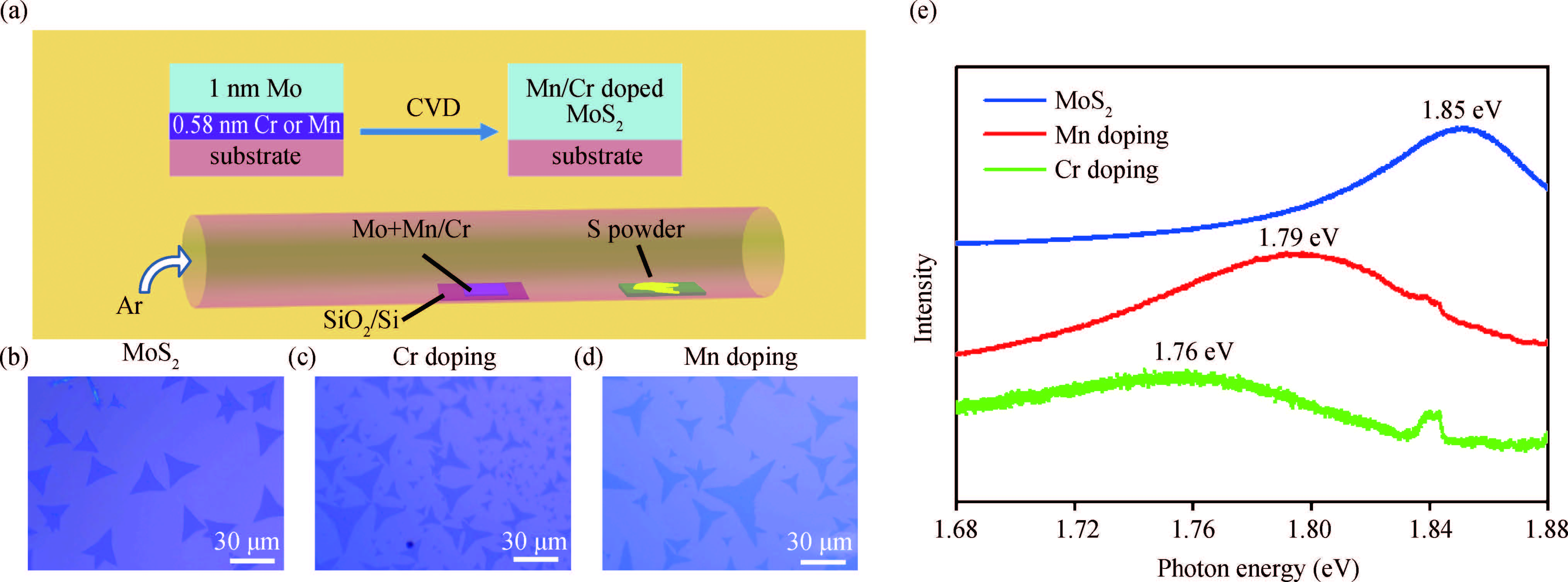
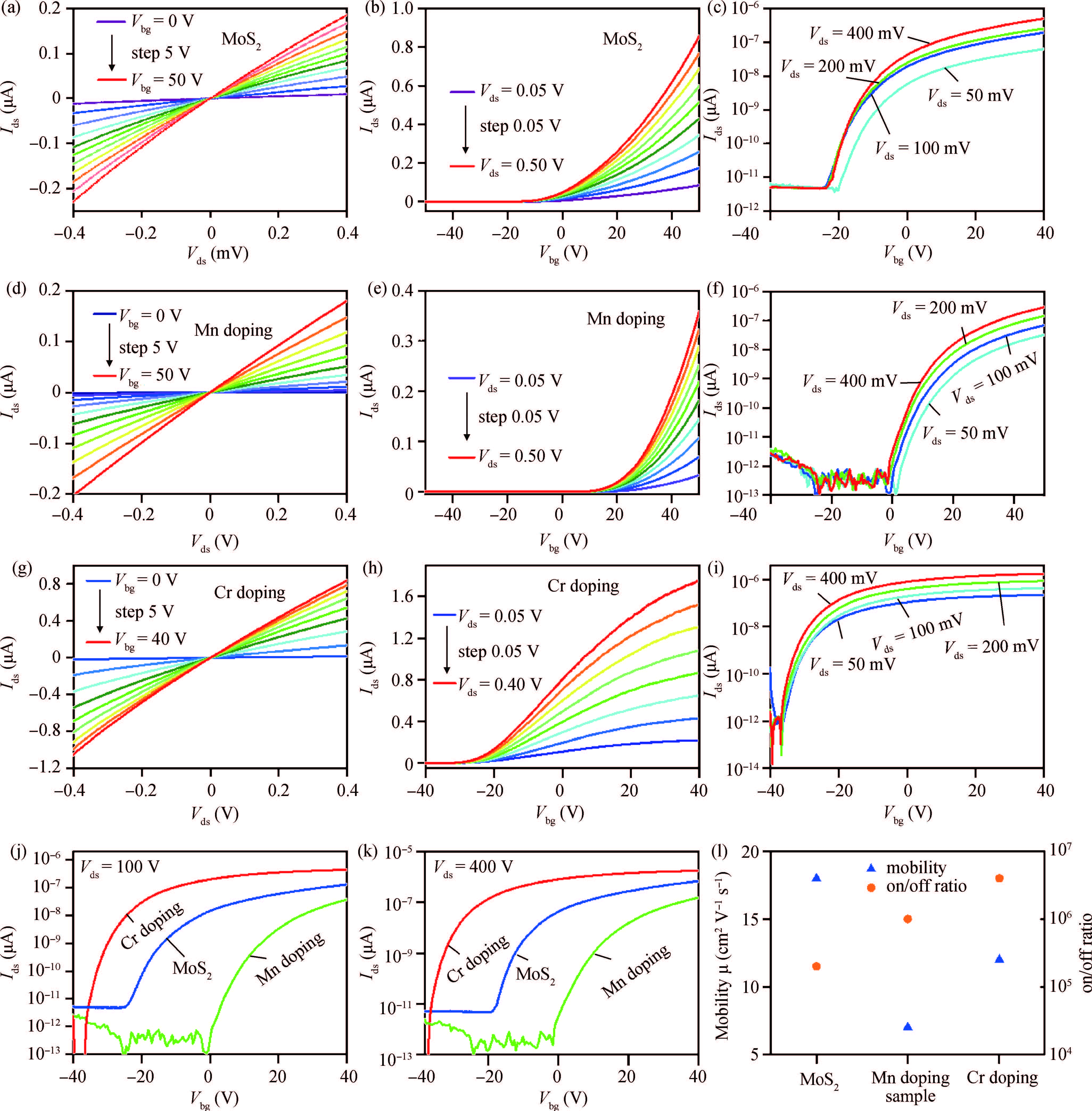
Abstract: Recently, two-dimensional materials have been attracting increasing attention because of their novel properties and promising applications. However, the impurity doping remains a significant challenge owing to the lack of the doping strategy in the atomically thin layers. Here we report on the chromium (Cr) and manganese (Mn) doping in atomically-thin MoS2 crystals grown by chemical vapor deposition. The Cr/Mn doped MoS2 samples are characterized by a peak at 1.76 and 1.79 eV in photoluminescence spectra, respectively, compared with the undoped one at 1.85 eV. The field-effect transistor (FET) devices based on the Mn doping show a higher threshold voltage than that of the pure MoS2 while the Cr doping exhibits the opposite behavior. Importantly, the carrier concentration in these samples displays a remarkable difference arising from the doping effect, consistent with the evolution of the FET performance. The temperature-dependent conductivity measurements further demonstrate a large variation in activation energy. The successful incorporation of the Mn and Cr impurities into the monolayer MoS2 paves the way towards the high Curie temperature two-dimensional dilute magnetic semiconductors.

Key words: MoS2field effect transistorsdilute magnetic semiconductorstwo-dimensional materials


[1]
Wang Q H, Kalantar-Zadeh K, Kis A, et al. Electronics and optoelectronics of two-dimensional transition metal dichalcogenides. Nat Nanotechnol, 2012, 7:699 doi: 10.1038/nnano.2012.193
[2]
Radisavljevic B, Kis A. Mobility engineering and a metalinsulator transition in monolayer MoS2. Nat Mater, 2013, 12:815 doi: 10.1038/nmat3687
[3]
Roy K, Padmanabhan M, Goswami S, et al. Graphene-MoS2 hybrid structures for multifunctional photoresponsive memory devices. Nat Nanotechnol, 2013, 8:826 doi: 10.1038/nnano.2013.206
[4]
Yu W J, Liu Y, Zhou H L, et al. Highly efficient gate-tunable photocurrent generation in vertical heterostructures of layered materials. Nat Nanotechnol, 2013, 8:952 doi: 10.1038/nnano.2013.219
[5]
Zhang Y, Oka T, Suzuki R, et al. Electrically switchable chiral light-emitting transistor. Science, 344:725 doi: 10.1126/science.1251329
[6]
Woods C R, Britnell L, Eckmann A, et al. Commensurateincommensurate transition in graphene on hexagonal boron nitride. Nat Phys, 2014, 10:451 doi: 10.1038/nphys2954
[7]
Wu S F, Ross J S, Liu G B, et al. Electrical tuning of valley magnetic moment through symmetry control in bilayer MoS2. Nat Phys, 2013, 9:149 doi: 10.1038/nphys2524
[8]
Xu X, Yao W, Xiao D, et al. Spin and pseudospins in layered transition metal dichalcogenides. Nat Phys, 2014, 10:343 doi: 10.1038/nphys2942
[9]
Young A F, Dean C R, Wang L, et al. Spin and valley quantum Hall ferromagnetism in graphene. Nat Phys, 2012, 8:550 doi: 10.1038/nphys2307
[10]
Peng L L, Peng X, Liu B R, et al. Ultrathin two-dimensional TS2/graphene hybrid nanostructures for high-performance, flexible planar supercapacitors. Nano Lett, 2013, 13:2151 doi: 10.1021/nl400600x
[11]
Pu J, Yomogida Y, Liu K K, et al. Highly flexible MoS2 thin-film transistors with ion gel dielectrics. Nano Lett, 2012, 12:4013 doi: 10.1021/nl301335q
[12]
Yoon J, Park W, Bae G, et al. Highly flexible and transparent multilayer MoS2 transistors with graphene electrodes. Small, 2013, 9:3295 https://www.researchgate.net/publication/283168907_Flexible_Electronics_Highly_Flexible_and_Transparent_Multilayer_MoS2_Transistors_with_Graphene_Electrodes_Small_192013
[13]
Lee G H, Yu Y J, Cui X, et al. Flexible and transparent MoS2 field-effect transistors on hexagonal boron nitride-graphene heterostructures. ACS Nano, 2013, 7:7931 doi: 10.1021/nn402954e
[14]
Chang H Y, Yang S X, Lee J H, et al. High-performance, highly bendable MoS2 transistors with high-k dielectrics for flexible low-power systems. ACS Nano, 2013, 7:5446 doi: 10.1021/nn401429w
[15]
Mak K F, Lee C, Hone J, et al. Atomically thin MoS2:a new direct-gap semiconductor. Phys Rev Lett, 2010, 105:136805 doi: 10.1103/PhysRevLett.105.136805
[16]
Bromley R, Murray R, Yoffe A. The band structures of some transition metal dichalcogenides. Ⅲ. Group VIA:trigonal prism materials. J Phys C, 1972, 5:759 doi: 10.1088/0022-3719/5/7/007
[17]
Mattheiss L. Band structures of transition-metal-dichalcogenide layer compounds. Phys Rev B, 1973, 8:3719 doi: 10.1103/PhysRevB.8.3719
[18]
Coehoorn R, Haas C, Dijkstra J, et al. Electronic structure of MoSe2, MoS2, and WSe2. I. Band-structure calculations and photoelectron spectroscopy. Phys Rev B, 1987, 35:6195 doi: 10.1103/PhysRevB.35.6195
[19]
Böer T, Severin R, Müler A, et al. Band structure of MoS2, MoSe2, and α-MoTe2:angle-resolved photoelectron spectroscopy and ab initio calculations. Phys Rev B, 2001, 64:235305 doi: 10.1103/PhysRevB.64.235305
[20]
Ganatra R, Zhang Q. Few-layer MoS2:a promising layered semiconductor. ACS Nano, 2014, 8(5):4074 doi: 10.1021/nn405938z
[21]
Lebegue S, Eriksson O. Electronic structure of two-dimensional crystals from ab initio theory. Phys Rev B, 2009, 79:115409 doi: 10.1103/PhysRevB.79.115409
[22]
Kuc A, Zibouche N, Heine T. Influence of quantum confinement on the electronic structure of the transition metal sulfide TS2. Phys Rev B, 2011, 83:245213 doi: 10.1103/PhysRevB.83.245213
[23]
Splendiani A, Sun L, Zhang Y B, et al. Emerging photoluminescence in monolayer MoS2. Nano Lett, 2010, 10:1271 doi: 10.1021/nl903868w
[24]
Schmidt H, Wang S F, Chu L Q, et al. Transport properties of monolayer MoS2 grown by chemical vapor deposition. Nano Lett, 2014, 14:1909 doi: 10.1021/nl4046922
[25]
Radisavljevic B, Radenovic A, Brivio J, et al. Single-layer MoS2 transistors. Nat Nanotechnol, 2011, 6:147 doi: 10.1038/nnano.2010.279
[26]
Lee Y H, Zhang X Q, Zhang W J, et al. Synthesis of large-area MoS2 atomic layers with chemical vapor deposition. Adv Mater, 2012, 24:2320 doi: 10.1002/adma.201104798
[27]
Ling X, Lee Y H, Lin Y X, et al. Role of the seeding promoter in MoS2 growth by chemical vapor deposition. Nano Lett, 2014, 14:464 doi: 10.1021/nl4033704
[28]
Zhan Y, Liu Z, Najmaei S, Ajayan P M, et al. Large-area vaporphase growth and characterization of MoS2 atomic layers on a SiO2 substrate. Small, 2012, 8:966 doi: 10.1002/smll.201102654
[29]
Wang S Y, Ko T S, Huang C C, et al. Optical and electrical properties of MoS2 and Fe-doped MoS2. Jpn J Appl Phys, 2014, 53:04EH07
[30]
Li B, Huang L, Zhong M Z, et al. Synthesis and transport properties of large-scale alloy Co0.16Mo0.84S2 bilayer nanosheets. ACS Nano, 2015, 9:1257 doi: 10.1021/nn505048y
[31]
Laskar M R, Nath D N, Ma L, et al. p-type doping of MoS2 thin films using Nb. Appl Phys Lett, 2014, 104:092104 doi: 10.1063/1.4867197
[32]
Fang H, Tosun M, Seol G, et al. Degenerate n-doping of fewlayer transition metal dichalcogenides by potassium. Nano Lett, 2013, 13:1991 doi: 10.1021/nl400044m
[33]
Priour D Jr, Hwang E, Sarma S D. Quasi-two-dimensional diluted magnetic semiconductor systems. Phys Rev Lett, 2005, 95:037201 doi: 10.1103/PhysRevLett.95.037201
[34]
Meilikhov E, Farzetdinova R. Quasi-two-dimensional diluted magnetic semiconductors with arbitrary carrier degeneracy. Phys Rev B, 2006, 74:125204 doi: 10.1103/PhysRevB.74.125204
[35]
Mishra R, Zhou W, Pennycook S J, et al. Long-range ferromagnetic ordering in manganese-doped two-dimensional dichalcogenides. Phys Rev B, 2013, 88:44409 https://www.researchgate.net/publication/258781938_Long-range_ferromagnetic_ordering_in_manganese-doped_two-dimensional_dichalcogenides
[36]
Ramasubramaniam A, Naveh D. Mn-doped monolayer MoS2:an atomically thin dilute magnetic semiconductor. Phys Rev B, 2013, 87:195201 doi: 10.1103/PhysRevB.87.195201
[37]
Huang Z Y, Peng X Y, Yang H, et al. The structural, electronic and magnetic properties of bi-layered MoS2 with transition-metals doped in the interlayer. RSC Adv, 2013, 3:12939 doi: 10.1039/c3ra41490f
[38]
Qi J, Li X, Chen X, et al. Strain tuning of magnetism in Mn doped MoS2 monolayer. J Phys Condensed Matter, 2014, 26:256003 doi: 10.1088/0953-8984/26/25/256003
[39]
Dietl T. A ten-year perspective on dilute magnetic semiconductors and oxides. Nat Mater, 2010, 9:965 doi: 10.1038/nmat2898
[40]
Ohno H, Shen A, Matsukura F, et al. (Ga,Mn)As:a new diluted magnetic semiconductor based on GaAs. Appl Phys Lett, 1996, 69:363 doi: 10.1063/1.118061
[41]
Zhang K, Feng S M, Wang J J, et al. Manganese doping of monolayer MoS2:the substrate is critical. Nano Lett 2015, 15:6586 doi: 10.1021/acs.nanolett.5b02315
[42]
Mak K F, He K L, Lee C G, et al. Tightly bound trions in monolayer MoS2. Nat Mater, 2013, 12:207
[43]
Liu H, Neal A T, Ye P D. Channel length scaling of MoS2 MOSFETs. ACS Nano, 2012, 6:8563 doi: 10.1021/nn303513c
[44]
Mak K F, He K, Shan J, et al. Control of valley polarization in monolayer MoS2 by optical helicity. Nat Nanotechnol, 2012, 7:494 doi: 10.1038/nnano.2012.96
[45]
Zeng H, Dai J, Yao W, et al. Valley polarization in MoS2 monolayers by optical pumping. Nat Nanotechnol, 2012, 7:490 doi: 10.1038/nnano.2012.95
[46]
Wu S, Ross J S, Liu G B, et al. Electrical tuning of valley magnetic moment through symmetry control in bilayer MoS2. Nat Phys, 2013, 9:149 doi: 10.1038/nphys2524
[47]
Suzuki R, Sakano M, Zhang Y J, et al. Valley-dependent spin polarization in bulk MoS2 with broken inversion symmetry. Nat Nanotechnol, 2014, 9:611 doi: 10.1038/nnano.2014.148
[48]
Najmaei S, Liu Z, Zhou W, et al. Vapour phase growth and grain boundary structure of molybdenum disulphide atomic layers. Nat Mater, 2014, 12:754 https://www.researchgate.net/profile/Zheng_Liu6/publication/255751114_nmat3673-s1/links/02e7e520a36f096cd5000000.pdf?inViewer=true&pdfJsDownload=true&disableCoverPage=true&origin=publication_detail
[49]
Mak K F, McGill K L, Park J, et al. The valley Hall effect in MoS2 transistors. Science, 2014, 344:1489 doi: 10.1126/science.1250140
[50]
Coehoorn R, Haas C, De Groot R. Electronic structure of MoSe2, MoS2, and WSe2. Ⅱ. The nature of the optical band gaps. Phys Rev B, 1987, 35:6203 doi: 10.1103/PhysRevB.35.6203
[51]
Wu M S, Xu B, Liu G, et al. First-principles study on the electronic structures of Cr-and W-doped single-layer MoS2. Acta Physica Sinica, 2013, 3:047
[52]
Andriotis A N, Menon M. Tunable magnetic properties of transition metal doped MoS2. Phys Rev B, 2014, 90:125304 doi: 10.1103/PhysRevB.90.125304
[53]
Conley H J, Wang B, Ziegler J I, et al. Bandgap engineering of strained monolayer and bilayer MoS2. Nano Lett, 2013, 13:3626 doi: 10.1021/nl4014748
[54]
Feng J, Qian X, Huang C W, et al. Strain-engineered artificial atom as a broad-spectrum solar energy funnel. Nat Photonics, 2012, 6:866 doi: 10.1038/nphoton.2012.285
[55]
Shi H, Pan H, Zhang Y W, et al. Quasiparticle band structures and optical properties of strained monolayer MoS2 and WS2. Phys Rev B, 2013, 87:155304 doi: 10.1103/PhysRevB.87.155304
[56]
Pan H, Zhang Y W. Tuning the electronic and magnetic properties of MoS2 nanoribbons by strain engineering. J Phys Chem C 2012, 116:11752 doi: 10.1021/jp3015782
[57]
Lu P, Wu X, Guo W, et al. Strain-dependent electronic and magnetic properties of MoS2 monolayer, bilayer, nanoribbons and nanotubes. Phys Chem Chem Phys, 2012, 14:13035 doi: 10.1039/c2cp42181j
[58]
Wang W Y, Liu Y W, Tang L, et al. Controllable Schottky barriers between MoS2 and permalloy. Sci Rep, 2014, 4:6928 doi: 10.1038/srep06928
[59]
Allain A, Kang J, Banerjee K, et al. Electrical contacts to twodimensional semiconductors. Nat Mater, 2015, 14:1195 doi: 10.1038/nmat4452
[60]
Fang F, Triebwasser S. Effect of surface scattering on electron mobility in an inversion layer on p-type silicon. Appl Phys Lett, 1964, 4:145 doi: 10.1063/1.1754005
[61]
Jariwala D, Sangwan V K, Late D J, et al. Band-like transport in high mobility unencapsulated single-layer MoS2 transistors. Appl Phys Lett, 2013, 102:173107 doi: 10.1063/1.4803920
[62]
Baugher B W, Churchill H O, Yang Y, et al. Intrinsic electronic transport properties of high-quality monolayer and bilayer MoS2. Nano Lett, 2013, 13:4212 doi: 10.1021/nl401916s
[63]
Komsa H P, Berseneva N, Krasheninnikov A V, et al. Charged point defects in the flatland:accurate formation energy calculations in two-dimensional materials. Phys Rev X, 2014, 4:031044 https://www.researchgate.net/publication/275323974_Charged_Point_Defects_in_the_Flatland_Accurate_Formation_Energy_Calculations_in_Two-Dimensional_Materials
[64]
Lee H S, Min S W, Chang Y G, et al. MoS2 Nanosheet phototransistors with thickness-modulated optical energy gap. Nano Lett, 2012, 12:3695 doi: 10.1021/nl301485q
[65]
Sze S M, Ng K K. Physics of semiconductor devices. John Wiley & Sons, 2006
[66]
Tian C, Chan S W. Electrical conductivities of (CeO2)1x-(Y2O3)x thin films. J Ame Ceramic Soc, 2002, 85:2222 doi: 10.1111/jace.2002.85.issue-9
[67]
Staebler D, Wronski C. Reversible conductivity changes in discharge-produced amorphous Si. Appl Phys Lett, 1977, 31:292 doi: 10.1063/1.89674
[68]
Ghatak S, Pal A N, Ghosh A. Nature of electronic states in atomically thin MoS2 field-effect transistors. ACS Nano, 2011, 5:7707 doi: 10.1021/nn202852j
Fig. 1.  (Color online) Schematic view of the synthesis and the optical properties of the samples. (a) A CVD growth process. Mn and Cr are used as the impurity dopants. (b)-(d) Optical images of the pure/Mn-doped/Cr-doped MoS2 on SiO2/Si substrate, respectively. (e) Photoluminescence spectra of three types of samples. Cr-doped MoS2 shows a strong photoluminescence at 1.76 eV while the Mn-doped MoS2 has a peak at 1.79 eV.

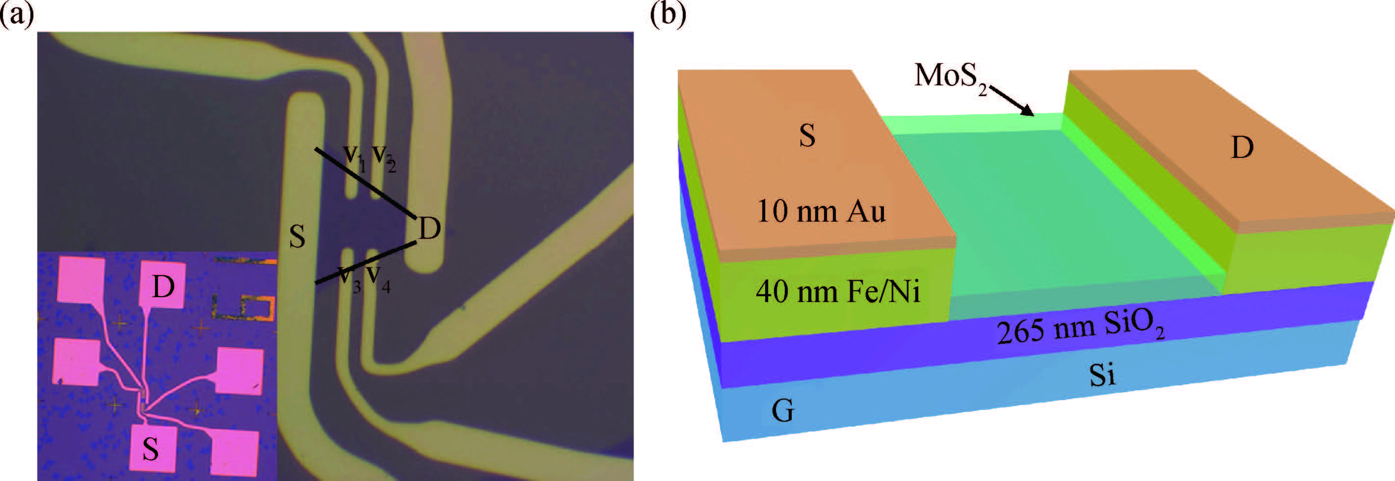
Fig. 2.  (Color online) Typical device configurations. (a) An optical image of the FET device (after metal deposition and lift-off). Permalloy/Gold were used for making source/drain electrodes. During the measurements, four-probe geometry wastaken to eliminate the contact resistance. The inset shows the overall morphology of the same device. (b) Three-dimensional schematic view of a typical transistor shown in (a).

Fig. 3.  (Color online) Room-temperature electrical properties of the FET devices. (a, d, g) Ids-Vds curves recorded at different Vbg of 0-50 V for the pure/Mn-doped/Cr-doped MoS2 FETs, respectively. The linear I-V curves indicate good Ohmic contacts. (b, e, h) Ids-Vbg curves at different Vsd of 50-500 mV. (c, f, i) Ids-Vbg curves plotted on a logarithmic scale. Gate leakage current is negligible. (j, k) A comparison of Ids-Vbg curves for the pure MoS2, Mn-doped, Cr-doped devices with Vds = 100 and 400 mV, respectively. (l) Summarized mobility and on/off ratio for three different FET devices. In general, the mobility decreases when MoS2 is doped with Cr while the on/off ratio is enhanced because of the reduced contact resistance.

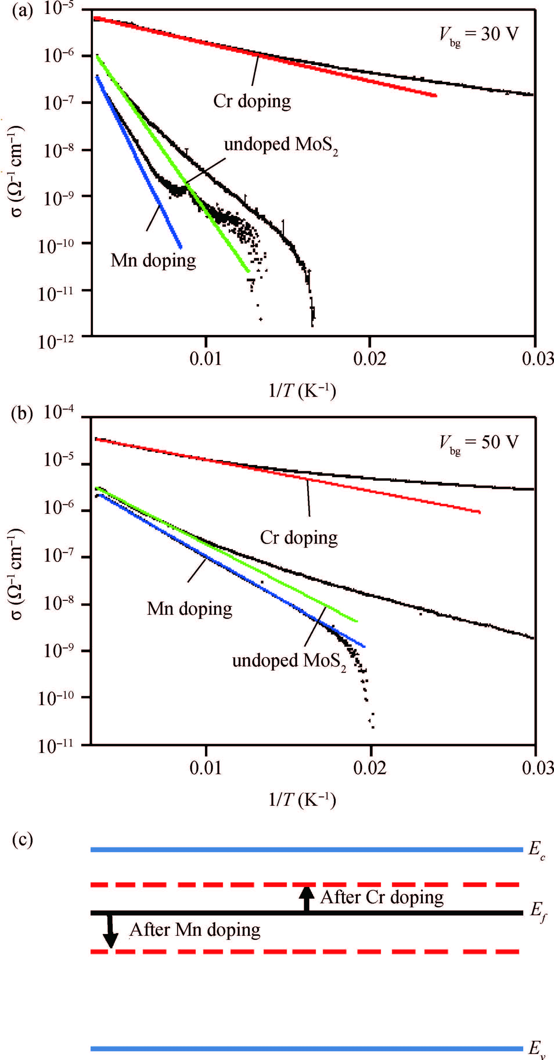
Fig. 4.  (Color online) Comparison of temperature-dependent conductivity and schematic drawing of a simplified band structure for MoS2 in the process of doping. (a, b) Arrhenius plots of conductivity for MoS2, Mn-doped, Cr-doped devices when Vbg = 30 and 50 V, respectively. Solid lines are the linear fits to extract the activation energy (Ea). When Vbg = 30 V, the activation energy is 69.1, 15.4, and 120 meV for the pure, Cr-doped and Mn-doped samples, respectively. Increasing the gate to 50 V, the Ea becomes 38.4, 14.1 and 41.7 meV for the three samples. (c) A simplified band structure to show the doping effect. Cr introduces donor levels while Mn moves the Ef towards valence band indicative of p-type-like doping, consistent with the theory[38, 51]

Table 1.   Device statistics.

Device L.(μm) W.(μm) μ (cm2V-1 s-1)Vth (V) n (cm-2)
Undoped-MoS2 113.5 6.0 18 -24 2:0 × 1012
Undoped-MoS2 28.4 5.1 31 -22 1:8 × 10¹²
Undoped-MoS2 311.5 6.0 5 -19 1:5 × 10¹²
Undoped-MoS2 412.8 5.8 8 -24 2:0 × 1012
Cr-doping 18.5 5.0 12 -37 3:0 × 1012
Cr-doping 29.4 9.5 8 -33 2:7 × 10¹²
Mn-doping 114.0 6.0 7 -2 1:6 × 10¹¹
Mn-doping 28.5 8.0 5 -9 7:3 × 10¹¹
Mn-doping 310.2 8.0 4 -10 8:1 × 10¹¹
DownLoad: CSV
[1]
Wang Q H, Kalantar-Zadeh K, Kis A, et al. Electronics and optoelectronics of two-dimensional transition metal dichalcogenides. Nat Nanotechnol, 2012, 7:699 doi: 10.1038/nnano.2012.193
[2]
Radisavljevic B, Kis A. Mobility engineering and a metalinsulator transition in monolayer MoS2. Nat Mater, 2013, 12:815 doi: 10.1038/nmat3687
[3]
Roy K, Padmanabhan M, Goswami S, et al. Graphene-MoS2 hybrid structures for multifunctional photoresponsive memory devices. Nat Nanotechnol, 2013, 8:826 doi: 10.1038/nnano.2013.206
[4]
Yu W J, Liu Y, Zhou H L, et al. Highly efficient gate-tunable photocurrent generation in vertical heterostructures of layered materials. Nat Nanotechnol, 2013, 8:952 doi: 10.1038/nnano.2013.219
[5]
Zhang Y, Oka T, Suzuki R, et al. Electrically switchable chiral light-emitting transistor. Science, 344:725 doi: 10.1126/science.1251329
[6]
Woods C R, Britnell L, Eckmann A, et al. Commensurateincommensurate transition in graphene on hexagonal boron nitride. Nat Phys, 2014, 10:451 doi: 10.1038/nphys2954
[7]
Wu S F, Ross J S, Liu G B, et al. Electrical tuning of valley magnetic moment through symmetry control in bilayer MoS2. Nat Phys, 2013, 9:149 doi: 10.1038/nphys2524
[8]
Xu X, Yao W, Xiao D, et al. Spin and pseudospins in layered transition metal dichalcogenides. Nat Phys, 2014, 10:343 doi: 10.1038/nphys2942
[9]
Young A F, Dean C R, Wang L, et al. Spin and valley quantum Hall ferromagnetism in graphene. Nat Phys, 2012, 8:550 doi: 10.1038/nphys2307
[10]
Peng L L, Peng X, Liu B R, et al. Ultrathin two-dimensional TS2/graphene hybrid nanostructures for high-performance, flexible planar supercapacitors. Nano Lett, 2013, 13:2151 doi: 10.1021/nl400600x
[11]
Pu J, Yomogida Y, Liu K K, et al. Highly flexible MoS2 thin-film transistors with ion gel dielectrics. Nano Lett, 2012, 12:4013 doi: 10.1021/nl301335q
[12]
Yoon J, Park W, Bae G, et al. Highly flexible and transparent multilayer MoS2 transistors with graphene electrodes. Small, 2013, 9:3295 https://www.researchgate.net/publication/283168907_Flexible_Electronics_Highly_Flexible_and_Transparent_Multilayer_MoS2_Transistors_with_Graphene_Electrodes_Small_192013
[13]
Lee G H, Yu Y J, Cui X, et al. Flexible and transparent MoS2 field-effect transistors on hexagonal boron nitride-graphene heterostructures. ACS Nano, 2013, 7:7931 doi: 10.1021/nn402954e
[14]
Chang H Y, Yang S X, Lee J H, et al. High-performance, highly bendable MoS2 transistors with high-k dielectrics for flexible low-power systems. ACS Nano, 2013, 7:5446 doi: 10.1021/nn401429w
[15]
Mak K F, Lee C, Hone J, et al. Atomically thin MoS2:a new direct-gap semiconductor. Phys Rev Lett, 2010, 105:136805 doi: 10.1103/PhysRevLett.105.136805
[16]
Bromley R, Murray R, Yoffe A. The band structures of some transition metal dichalcogenides. Ⅲ. Group VIA:trigonal prism materials. J Phys C, 1972, 5:759 doi: 10.1088/0022-3719/5/7/007
[17]
Mattheiss L. Band structures of transition-metal-dichalcogenide layer compounds. Phys Rev B, 1973, 8:3719 doi: 10.1103/PhysRevB.8.3719
[18]
Coehoorn R, Haas C, Dijkstra J, et al. Electronic structure of MoSe2, MoS2, and WSe2. I. Band-structure calculations and photoelectron spectroscopy. Phys Rev B, 1987, 35:6195 doi: 10.1103/PhysRevB.35.6195
[19]
Böer T, Severin R, Müler A, et al. Band structure of MoS2, MoSe2, and α-MoTe2:angle-resolved photoelectron spectroscopy and ab initio calculations. Phys Rev B, 2001, 64:235305 doi: 10.1103/PhysRevB.64.235305
[20]
Ganatra R, Zhang Q. Few-layer MoS2:a promising layered semiconductor. ACS Nano, 2014, 8(5):4074 doi: 10.1021/nn405938z
[21]
Lebegue S, Eriksson O. Electronic structure of two-dimensional crystals from ab initio theory. Phys Rev B, 2009, 79:115409 doi: 10.1103/PhysRevB.79.115409
[22]
Kuc A, Zibouche N, Heine T. Influence of quantum confinement on the electronic structure of the transition metal sulfide TS2. Phys Rev B, 2011, 83:245213 doi: 10.1103/PhysRevB.83.245213
[23]
Splendiani A, Sun L, Zhang Y B, et al. Emerging photoluminescence in monolayer MoS2. Nano Lett, 2010, 10:1271 doi: 10.1021/nl903868w
[24]
Schmidt H, Wang S F, Chu L Q, et al. Transport properties of monolayer MoS2 grown by chemical vapor deposition. Nano Lett, 2014, 14:1909 doi: 10.1021/nl4046922
[25]
Radisavljevic B, Radenovic A, Brivio J, et al. Single-layer MoS2 transistors. Nat Nanotechnol, 2011, 6:147 doi: 10.1038/nnano.2010.279
[26]
Lee Y H, Zhang X Q, Zhang W J, et al. Synthesis of large-area MoS2 atomic layers with chemical vapor deposition. Adv Mater, 2012, 24:2320 doi: 10.1002/adma.201104798
[27]
Ling X, Lee Y H, Lin Y X, et al. Role of the seeding promoter in MoS2 growth by chemical vapor deposition. Nano Lett, 2014, 14:464 doi: 10.1021/nl4033704
[28]
Zhan Y, Liu Z, Najmaei S, Ajayan P M, et al. Large-area vaporphase growth and characterization of MoS2 atomic layers on a SiO2 substrate. Small, 2012, 8:966 doi: 10.1002/smll.201102654
[29]
Wang S Y, Ko T S, Huang C C, et al. Optical and electrical properties of MoS2 and Fe-doped MoS2. Jpn J Appl Phys, 2014, 53:04EH07
[30]
Li B, Huang L, Zhong M Z, et al. Synthesis and transport properties of large-scale alloy Co0.16Mo0.84S2 bilayer nanosheets. ACS Nano, 2015, 9:1257 doi: 10.1021/nn505048y
[31]
Laskar M R, Nath D N, Ma L, et al. p-type doping of MoS2 thin films using Nb. Appl Phys Lett, 2014, 104:092104 doi: 10.1063/1.4867197
[32]
Fang H, Tosun M, Seol G, et al. Degenerate n-doping of fewlayer transition metal dichalcogenides by potassium. Nano Lett, 2013, 13:1991 doi: 10.1021/nl400044m
[33]
Priour D Jr, Hwang E, Sarma S D. Quasi-two-dimensional diluted magnetic semiconductor systems. Phys Rev Lett, 2005, 95:037201 doi: 10.1103/PhysRevLett.95.037201
[34]
Meilikhov E, Farzetdinova R. Quasi-two-dimensional diluted magnetic semiconductors with arbitrary carrier degeneracy. Phys Rev B, 2006, 74:125204 doi: 10.1103/PhysRevB.74.125204
[35]
Mishra R, Zhou W, Pennycook S J, et al. Long-range ferromagnetic ordering in manganese-doped two-dimensional dichalcogenides. Phys Rev B, 2013, 88:44409 https://www.researchgate.net/publication/258781938_Long-range_ferromagnetic_ordering_in_manganese-doped_two-dimensional_dichalcogenides
[36]
Ramasubramaniam A, Naveh D. Mn-doped monolayer MoS2:an atomically thin dilute magnetic semiconductor. Phys Rev B, 2013, 87:195201 doi: 10.1103/PhysRevB.87.195201
[37]
Huang Z Y, Peng X Y, Yang H, et al. The structural, electronic and magnetic properties of bi-layered MoS2 with transition-metals doped in the interlayer. RSC Adv, 2013, 3:12939 doi: 10.1039/c3ra41490f
[38]
Qi J, Li X, Chen X, et al. Strain tuning of magnetism in Mn doped MoS2 monolayer. J Phys Condensed Matter, 2014, 26:256003 doi: 10.1088/0953-8984/26/25/256003
[39]
Dietl T. A ten-year perspective on dilute magnetic semiconductors and oxides. Nat Mater, 2010, 9:965 doi: 10.1038/nmat2898
[40]
Ohno H, Shen A, Matsukura F, et al. (Ga,Mn)As:a new diluted magnetic semiconductor based on GaAs. Appl Phys Lett, 1996, 69:363 doi: 10.1063/1.118061
[41]
Zhang K, Feng S M, Wang J J, et al. Manganese doping of monolayer MoS2:the substrate is critical. Nano Lett 2015, 15:6586 doi: 10.1021/acs.nanolett.5b02315
[42]
Mak K F, He K L, Lee C G, et al. Tightly bound trions in monolayer MoS2. Nat Mater, 2013, 12:207
[43]
Liu H, Neal A T, Ye P D. Channel length scaling of MoS2 MOSFETs. ACS Nano, 2012, 6:8563 doi: 10.1021/nn303513c
[44]
Mak K F, He K, Shan J, et al. Control of valley polarization in monolayer MoS2 by optical helicity. Nat Nanotechnol, 2012, 7:494 doi: 10.1038/nnano.2012.96
[45]
Zeng H, Dai J, Yao W, et al. Valley polarization in MoS2 monolayers by optical pumping. Nat Nanotechnol, 2012, 7:490 doi: 10.1038/nnano.2012.95
[46]
Wu S, Ross J S, Liu G B, et al. Electrical tuning of valley magnetic moment through symmetry control in bilayer MoS2. Nat Phys, 2013, 9:149 doi: 10.1038/nphys2524
[47]
Suzuki R, Sakano M, Zhang Y J, et al. Valley-dependent spin polarization in bulk MoS2 with broken inversion symmetry. Nat Nanotechnol, 2014, 9:611 doi: 10.1038/nnano.2014.148
[48]
Najmaei S, Liu Z, Zhou W, et al. Vapour phase growth and grain boundary structure of molybdenum disulphide atomic layers. Nat Mater, 2014, 12:754 https://www.researchgate.net/profile/Zheng_Liu6/publication/255751114_nmat3673-s1/links/02e7e520a36f096cd5000000.pdf?inViewer=true&pdfJsDownload=true&disableCoverPage=true&origin=publication_detail
[49]
Mak K F, McGill K L, Park J, et al. The valley Hall effect in MoS2 transistors. Science, 2014, 344:1489 doi: 10.1126/science.1250140
[50]
Coehoorn R, Haas C, De Groot R. Electronic structure of MoSe2, MoS2, and WSe2. Ⅱ. The nature of the optical band gaps. Phys Rev B, 1987, 35:6203 doi: 10.1103/PhysRevB.35.6203
[51]
Wu M S, Xu B, Liu G, et al. First-principles study on the electronic structures of Cr-and W-doped single-layer MoS2. Acta Physica Sinica, 2013, 3:047
[52]
Andriotis A N, Menon M. Tunable magnetic properties of transition metal doped MoS2. Phys Rev B, 2014, 90:125304 doi: 10.1103/PhysRevB.90.125304
[53]
Conley H J, Wang B, Ziegler J I, et al. Bandgap engineering of strained monolayer and bilayer MoS2. Nano Lett, 2013, 13:3626 doi: 10.1021/nl4014748
[54]
Feng J, Qian X, Huang C W, et al. Strain-engineered artificial atom as a broad-spectrum solar energy funnel. Nat Photonics, 2012, 6:866 doi: 10.1038/nphoton.2012.285
[55]
Shi H, Pan H, Zhang Y W, et al. Quasiparticle band structures and optical properties of strained monolayer MoS2 and WS2. Phys Rev B, 2013, 87:155304 doi: 10.1103/PhysRevB.87.155304
[56]
Pan H, Zhang Y W. Tuning the electronic and magnetic properties of MoS2 nanoribbons by strain engineering. J Phys Chem C 2012, 116:11752 doi: 10.1021/jp3015782
[57]
Lu P, Wu X, Guo W, et al. Strain-dependent electronic and magnetic properties of MoS2 monolayer, bilayer, nanoribbons and nanotubes. Phys Chem Chem Phys, 2012, 14:13035 doi: 10.1039/c2cp42181j
[58]
Wang W Y, Liu Y W, Tang L, et al. Controllable Schottky barriers between MoS2 and permalloy. Sci Rep, 2014, 4:6928 doi: 10.1038/srep06928
[59]
Allain A, Kang J, Banerjee K, et al. Electrical contacts to twodimensional semiconductors. Nat Mater, 2015, 14:1195 doi: 10.1038/nmat4452
[60]
Fang F, Triebwasser S. Effect of surface scattering on electron mobility in an inversion layer on p-type silicon. Appl Phys Lett, 1964, 4:145 doi: 10.1063/1.1754005
[61]
Jariwala D, Sangwan V K, Late D J, et al. Band-like transport in high mobility unencapsulated single-layer MoS2 transistors. Appl Phys Lett, 2013, 102:173107 doi: 10.1063/1.4803920
[62]
Baugher B W, Churchill H O, Yang Y, et al. Intrinsic electronic transport properties of high-quality monolayer and bilayer MoS2. Nano Lett, 2013, 13:4212 doi: 10.1021/nl401916s
[63]
Komsa H P, Berseneva N, Krasheninnikov A V, et al. Charged point defects in the flatland:accurate formation energy calculations in two-dimensional materials. Phys Rev X, 2014, 4:031044 https://www.researchgate.net/publication/275323974_Charged_Point_Defects_in_the_Flatland_Accurate_Formation_Energy_Calculations_in_Two-Dimensional_Materials
[64]
Lee H S, Min S W, Chang Y G, et al. MoS2 Nanosheet phototransistors with thickness-modulated optical energy gap. Nano Lett, 2012, 12:3695 doi: 10.1021/nl301485q
[65]
Sze S M, Ng K K. Physics of semiconductor devices. John Wiley & Sons, 2006
[66]
Tian C, Chan S W. Electrical conductivities of (CeO2)1x-(Y2O3)x thin films. J Ame Ceramic Soc, 2002, 85:2222 doi: 10.1111/jace.2002.85.issue-9
[67]
Staebler D, Wronski C. Reversible conductivity changes in discharge-produced amorphous Si. Appl Phys Lett, 1977, 31:292 doi: 10.1063/1.89674
[68]
Ghatak S, Pal A N, Ghosh A. Nature of electronic states in atomically thin MoS2 field-effect transistors. ACS Nano, 2011, 5:7707 doi: 10.1021/nn202852j
  • Search

    Advanced Search >>

    GET CITATION

    shu

    Export: BibTex EndNote

    Article Metrics

    Article views: 4729 Times PDF downloads: 81 Times Cited by: 0 Times

    History

    Received: 22 August 2016 Revised: 01 November 2016 Online: Published: 01 March 2017

    Catalog

      Email This Article

      User name:
      Email:*请输入正确邮箱
      Code:*验证码错误
      Ce Huang, Yibo Jin, Weiyi Wang, Lei Tang, Chaoyu Song, Faxian Xiu. Manganese and chromium doping in atomically thin MoS2[J]. Journal of Semiconductors, 2017, 38(3): 033004. doi: 10.1088/1674-4926/38/3/033004 ****C Huang, Y B Jin, W Y Wang, L Tang, C Y Song, F X Xiu. Manganese and chromium doping in atomically thin MoS2[J]. J. Semicond., 2017, 38(3): 033004. doi: 10.1088/1674-4926/38/3/033004.
      Citation:
      Ce Huang, Yibo Jin, Weiyi Wang, Lei Tang, Chaoyu Song, Faxian Xiu. Manganese and chromium doping in atomically thin MoS2[J]. Journal of Semiconductors, 2017, 38(3): 033004. doi: 10.1088/1674-4926/38/3/033004 ****
      C Huang, Y B Jin, W Y Wang, L Tang, C Y Song, F X Xiu. Manganese and chromium doping in atomically thin MoS2[J]. J. Semicond., 2017, 38(3): 033004. doi: 10.1088/1674-4926/38/3/033004.

      Manganese and chromium doping in atomically thin MoS2

      doi: 10.1088/1674-4926/38/3/033004
      Funds:

      the Chinese National Science Fund for Talent Training in Basic Science No.J1103204

      Project supported by the National Young 1000 Talent Plan,the Pujiang Talent Plan in Shanghai,the National Natural Science Foundation of China Nos.61322407,11474058,61674040

      Project supported by the National Young 1000 Talent Plan, the Pujiang Talent Plan in Shanghai, the National Natural Science Foundation of China (Nos.61322407,11474058,61674040), and the Chinese National Science Fund for Talent Training in Basic Science (No.J1103204).

      More Information
      • Corresponding author: Email:Faxian@fudan.edu.cn
      • Received Date: 2016-08-22
      • Revised Date: 2016-11-01
      • Published Date: 2017-03-01

      Catalog

        /

        DownLoad:  Full-Size Img  PowerPoint
        Return
        Return