


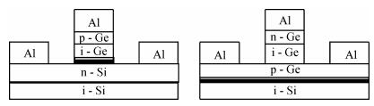
Fig. 1.
(Color online) Schematic of two kinds of Si-based Ge PDs (the red region is LT-Ge layer).
SEMICONDUCTOR PHYSICS
Xiaohui Yi, Zhiwei Huang, Guangyang Lin, Cheng Li, Songyan Chen, Wei Huang, Jun Li and Jianyuan Wang
Corresponding author: Li Cheng, Email: lich@xmu.edu.cn
Abstract: The influence of defects in low temperature Ge layer on electrical characteristics of p-Ge/i-Ge/n-Si and n-Ge/i-Ge/p-Ge photodiodes (PDs) was studied. Due to a two-step growth method, there are high defect densities in low-temperature buffer Ge layer. It is shown that the defects in low-temperature Ge layer change the band diagrams and the distribution of electric field, leading to the increase of the total dark current for p-Ge/i-Ge/n-Si PDs, whereas these defects have no influence on the dark current for n-Ge/i-Ge/p-Ge PDs. As a complement, a three-dimensional simulation of the total current under illumination was also performed.
Keywords: germanium, photodiodes, defects, dark current, simulation
| [1] |
Feng S Z, Liao S R, Dong P, et al. High-speed Ge photodetector monolithically integrated with large cross-section silicon-on insulator waveguide. Appl Phys Lett, 2009, 95(26): 261105 doi: 10.1063/1.3279129
|
| [2] |
Colace L, Masini G, Assanto G. Ge-on-Si approaches to the detection of near-infrared light. IEEE J Quantum Electron, 2002, 35(12): 1843
|
| [3] |
Kang Y, Liu H D, Morse M, et al. Monolithic germanium/silicon avalanche PDs with 340 GHz gain-bandwidth product. Nat Photonics, 2009, 3: 59 doi: 10.1038/nphoton.2008.247
|
| [4] |
Kanbe H, Miyaji M, Ito T. Ge/Si heterojunction photodiodes fabricated by low temperature wafer bonding. Appl Phys Express, 2008, 1(7): 072301 https://www.researchgate.net/profile/Farzan_Gity/publication/255789260_GeSi_heterojunction_photodiodes_fabricated_by_low_temperature_wafer_bonding/links/53f481020cf22be01c3ec7b7.pdf?origin=publication_detail
|
| [5] |
Cheng B W, Xue H Y, Hu D, et al. Low threading-dislocation-density Ge film on Si grown on a pitting Ge buffer layer. 5th IEEE International Conference on Group Ⅳ Photonics, 2008: 140
|
| [6] |
Yu H Y, Park J H, Okyay A K, et al. Selective-area high-quality germanium growth for monolithic integrated optoelectronics. IEEE Electron Device Lett, 2012, 33(4): 579 doi: 10.1109/LED.2011.2181814
|
| [7] |
PGrillot P N, Ringel S A. Minority-and majority-carrier trapping in strain-relaxed Ge0.3Si0.7/Si heterostructure diodes grown by rapid thermal chemical-vapor deposition. J Appl Phys, 1995, 77(2): 676 doi: 10.1063/1.359054
|
| [8] |
Giovane L M, Luan H C, Agarwal A M, et al. Correlation between leakage current density and threading dislocation density in SiGe p-i-n diodes grown on relaxed graded buffer layers. Appl Phys Lett, 2001, 78(4): 541 doi: 10.1063/1.1341230
|
| [9] |
Ang K W, Ng J W, Lo G Q, et al. The impact of field-enhanced band-traps-band tunneling on the dark current generation in Germanium. Appl Phys Lett, 2009, 94(22): 223515 doi: 10.1063/1.3151913
|
| [10] |
Tsipas P, Dimoulas A. Modeling of negatively charged states at the Ge surface and interface. Appl Phys Lett, 2009, 94(1): 012114 doi: 10.1063/1.3068497
|
| [11] |
Kuzum D, Martens K, Krishnamohan T, et al. Characteristics of surface states and charge neutrality level in Ge. Appl Phys Lett, 2009, 95: 252101 doi: 10.1063/1.3270529
|
| [12] |
Wang X L, Xiang J J, Wang W W, et al. Investigation on the dominant key to achieve superior Ge surface passivation by GeOx based on the ozone oxidation. Appl Surf Sci, 2015, 357: 1857 doi: 10.1016/j.apsusc.2015.09.084
|
| [13] |
Wang C, Li C, Wei J B, et al. High performance Ge p-n photodiode achieved with pre-annealing and excimer laser annealing. IEEE Photonics Technol Lett, 2015, 27(14): 1485 doi: 10.1109/LPT.2015.2426016
|
| [14] |
Selberherr S. Analysis and simulation of semiconductor devices. New York: Springer-Verlag, 1984
|
| [15] |
Simmons J G, Taylor G W. Nonequilibrium steady-state statistics and associated effects for insulators and semiconductors containing an arbitrary distribution of traps. Phys Rev B, 1971, 4(2): 502 doi: 10.1103/PhysRevB.4.502
|
| [16] |
White W T, Dease C G, Pocha M D. Modeling GaAs high-voltage, subnanosecond photoconductive switches in one spatial dimension. IEEE Trans Electron Devices, 1990, 37: 2532 doi: 10.1109/16.64530
|
| [17] |
Yang J H, Wei Y, Cai X Y, et al. The effects of threading dislocations and tensile strain in Ge/Si photodetector. Microelectron Int, 2010, 27(2): 113 doi: 10.1108/13565361011034803
|
| [18] |
Loo R, Wang G, Souriau L, et al. High quality Ge virtual substrates on Si wafers with standard STI patterning. J Electrochem Soc, 2010, 164(1): H13 https://www.researchgate.net/publication/234871266_High_Quality_Ge_Virtual_Substrates_on_Si_Wafers_with_Standard_STI_Patterning
|
| [19] |
Zistl C, Sieleman R, Hasslein H, et al. DLTS combined with perturbed angular correlation (PAC) on radioactive In-111 atoms in Ge. Mater Sci Forum, 1997, 258-263: 53 doi: 10.4028/www.scientific.net/MSF.258-263
|
| [20] |
Spiewak P, Vanhellemont J, Sueoka K, et al. First principles calculations of the formation energy and deep levels associated with the neutral and charged vacancy in germanium. J Appl Phys, 2008, 103(8): 086103 doi: 10.1063/1.2907730
|
| [21] |
Tahini H, Chroneos A, Grimes R W, et al. Diffusion of E centers in germanium predicted using GGA+U approach. Appl Phys Lett, 2011, 99(7): 072112 doi: 10.1063/1.3625939
|
| [22] |
Shah V A, Dobbie A, Myronov M, et al. Effect of layer thickness on structural quality of Ge epilayers grown directly on Si (001). Thin Solid Films, 2011, 519(22): 7911 doi: 10.1016/j.tsf.2011.06.022
|
| [23] |
Chroneos A, Bracht H, Grimes R W, et al. Vacancy-mediated dopant diffusion activation enthalpies for germanium. Appl Phys Lett, 2008, 92(17): 172103 doi: 10.1063/1.2918842
|
| [24] |
Brotzmann S, Bracht H. Intrinsic and extrinsic diffusion of phosphorus, arsenic, and antimony in germanium. J Appl Phys, 2008, 103(3): 033508 doi: 10.1063/1.2837103
|
| [25] |
Logan D F, Jessop P E, Knights A P. modeling defect enhanced detection at 1550 nm in integrated silicon waveguide photodetectors. J Lightw Technol, 2009, 27(7): 930 doi: 10.1109/JLT.2008.927752
|
| [26] |
Li C, Xue C L, Li Y M, et al. High performance silicon waveguide germanium photodetector. Chin Phys B, 2015, 24(3): 038502 doi: 10.1088/1674-1056/24/3/038502
|
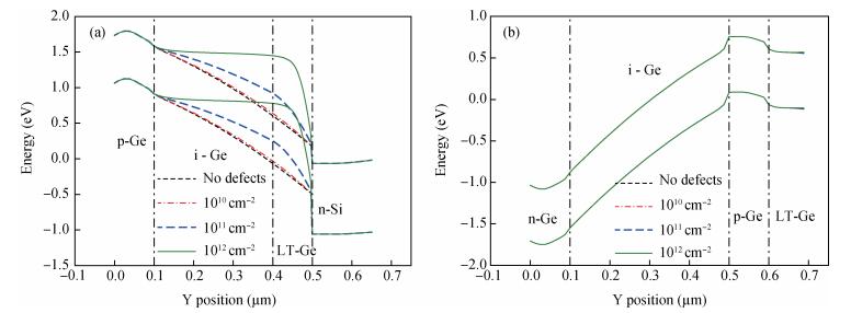
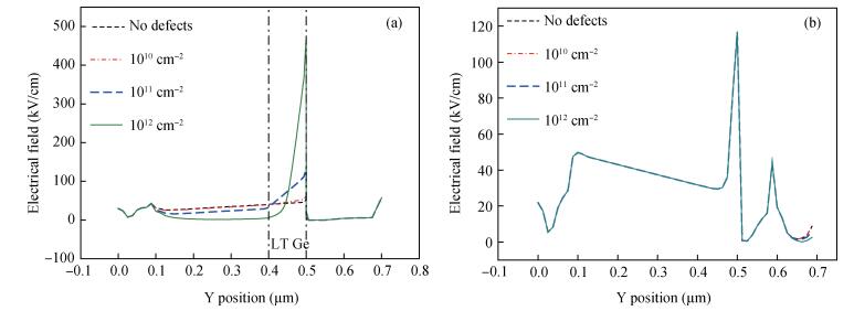
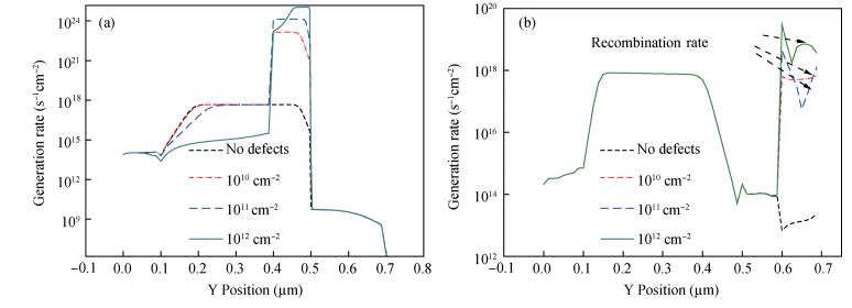
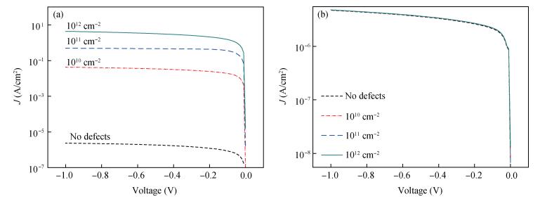
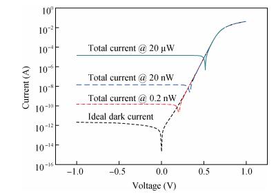
Table 1. The thickness and doping concentration of structures A and B.

|
| [1] |
Feng S Z, Liao S R, Dong P, et al. High-speed Ge photodetector monolithically integrated with large cross-section silicon-on insulator waveguide. Appl Phys Lett, 2009, 95(26): 261105 doi: 10.1063/1.3279129
|
| [2] |
Colace L, Masini G, Assanto G. Ge-on-Si approaches to the detection of near-infrared light. IEEE J Quantum Electron, 2002, 35(12): 1843
|
| [3] |
Kang Y, Liu H D, Morse M, et al. Monolithic germanium/silicon avalanche PDs with 340 GHz gain-bandwidth product. Nat Photonics, 2009, 3: 59 doi: 10.1038/nphoton.2008.247
|
| [4] |
Kanbe H, Miyaji M, Ito T. Ge/Si heterojunction photodiodes fabricated by low temperature wafer bonding. Appl Phys Express, 2008, 1(7): 072301 https://www.researchgate.net/profile/Farzan_Gity/publication/255789260_GeSi_heterojunction_photodiodes_fabricated_by_low_temperature_wafer_bonding/links/53f481020cf22be01c3ec7b7.pdf?origin=publication_detail
|
| [5] |
Cheng B W, Xue H Y, Hu D, et al. Low threading-dislocation-density Ge film on Si grown on a pitting Ge buffer layer. 5th IEEE International Conference on Group Ⅳ Photonics, 2008: 140
|
| [6] |
Yu H Y, Park J H, Okyay A K, et al. Selective-area high-quality germanium growth for monolithic integrated optoelectronics. IEEE Electron Device Lett, 2012, 33(4): 579 doi: 10.1109/LED.2011.2181814
|
| [7] |
PGrillot P N, Ringel S A. Minority-and majority-carrier trapping in strain-relaxed Ge0.3Si0.7/Si heterostructure diodes grown by rapid thermal chemical-vapor deposition. J Appl Phys, 1995, 77(2): 676 doi: 10.1063/1.359054
|
| [8] |
Giovane L M, Luan H C, Agarwal A M, et al. Correlation between leakage current density and threading dislocation density in SiGe p-i-n diodes grown on relaxed graded buffer layers. Appl Phys Lett, 2001, 78(4): 541 doi: 10.1063/1.1341230
|
| [9] |
Ang K W, Ng J W, Lo G Q, et al. The impact of field-enhanced band-traps-band tunneling on the dark current generation in Germanium. Appl Phys Lett, 2009, 94(22): 223515 doi: 10.1063/1.3151913
|
| [10] |
Tsipas P, Dimoulas A. Modeling of negatively charged states at the Ge surface and interface. Appl Phys Lett, 2009, 94(1): 012114 doi: 10.1063/1.3068497
|
| [11] |
Kuzum D, Martens K, Krishnamohan T, et al. Characteristics of surface states and charge neutrality level in Ge. Appl Phys Lett, 2009, 95: 252101 doi: 10.1063/1.3270529
|
| [12] |
Wang X L, Xiang J J, Wang W W, et al. Investigation on the dominant key to achieve superior Ge surface passivation by GeOx based on the ozone oxidation. Appl Surf Sci, 2015, 357: 1857 doi: 10.1016/j.apsusc.2015.09.084
|
| [13] |
Wang C, Li C, Wei J B, et al. High performance Ge p-n photodiode achieved with pre-annealing and excimer laser annealing. IEEE Photonics Technol Lett, 2015, 27(14): 1485 doi: 10.1109/LPT.2015.2426016
|
| [14] |
Selberherr S. Analysis and simulation of semiconductor devices. New York: Springer-Verlag, 1984
|
| [15] |
Simmons J G, Taylor G W. Nonequilibrium steady-state statistics and associated effects for insulators and semiconductors containing an arbitrary distribution of traps. Phys Rev B, 1971, 4(2): 502 doi: 10.1103/PhysRevB.4.502
|
| [16] |
White W T, Dease C G, Pocha M D. Modeling GaAs high-voltage, subnanosecond photoconductive switches in one spatial dimension. IEEE Trans Electron Devices, 1990, 37: 2532 doi: 10.1109/16.64530
|
| [17] |
Yang J H, Wei Y, Cai X Y, et al. The effects of threading dislocations and tensile strain in Ge/Si photodetector. Microelectron Int, 2010, 27(2): 113 doi: 10.1108/13565361011034803
|
| [18] |
Loo R, Wang G, Souriau L, et al. High quality Ge virtual substrates on Si wafers with standard STI patterning. J Electrochem Soc, 2010, 164(1): H13 https://www.researchgate.net/publication/234871266_High_Quality_Ge_Virtual_Substrates_on_Si_Wafers_with_Standard_STI_Patterning
|
| [19] |
Zistl C, Sieleman R, Hasslein H, et al. DLTS combined with perturbed angular correlation (PAC) on radioactive In-111 atoms in Ge. Mater Sci Forum, 1997, 258-263: 53 doi: 10.4028/www.scientific.net/MSF.258-263
|
| [20] |
Spiewak P, Vanhellemont J, Sueoka K, et al. First principles calculations of the formation energy and deep levels associated with the neutral and charged vacancy in germanium. J Appl Phys, 2008, 103(8): 086103 doi: 10.1063/1.2907730
|
| [21] |
Tahini H, Chroneos A, Grimes R W, et al. Diffusion of E centers in germanium predicted using GGA+U approach. Appl Phys Lett, 2011, 99(7): 072112 doi: 10.1063/1.3625939
|
| [22] |
Shah V A, Dobbie A, Myronov M, et al. Effect of layer thickness on structural quality of Ge epilayers grown directly on Si (001). Thin Solid Films, 2011, 519(22): 7911 doi: 10.1016/j.tsf.2011.06.022
|
| [23] |
Chroneos A, Bracht H, Grimes R W, et al. Vacancy-mediated dopant diffusion activation enthalpies for germanium. Appl Phys Lett, 2008, 92(17): 172103 doi: 10.1063/1.2918842
|
| [24] |
Brotzmann S, Bracht H. Intrinsic and extrinsic diffusion of phosphorus, arsenic, and antimony in germanium. J Appl Phys, 2008, 103(3): 033508 doi: 10.1063/1.2837103
|
| [25] |
Logan D F, Jessop P E, Knights A P. modeling defect enhanced detection at 1550 nm in integrated silicon waveguide photodetectors. J Lightw Technol, 2009, 27(7): 930 doi: 10.1109/JLT.2008.927752
|
| [26] |
Li C, Xue C L, Li Y M, et al. High performance silicon waveguide germanium photodetector. Chin Phys B, 2015, 24(3): 038502 doi: 10.1088/1674-1056/24/3/038502
|


Article views: 3801 Times PDF downloads: 56 Times Cited by: 0 Times
Received: 12 September 2016 Revised: 17 October 2016 Online: Published: 01 April 2017
| Citation: |
Xiaohui Yi, Zhiwei Huang, Guangyang Lin, Cheng Li, Songyan Chen, Wei Huang, Jun Li, Jianyuan Wang. Simulation of the effects of defects in low temperature Ge buffer layer on dark current of Si-based Ge photodiodes[J]. Journal of Semiconductors, 2017, 38(4): 042001. doi: 10.1088/1674-4926/38/4/042001
****
X H Yi, Z W Huang, G Y Lin, C Li, S Y Chen, W Huang, J Li, J Y Wang. Simulation of the effects of defects in low temperature Ge buffer layer on dark current of Si-based Ge photodiodes[J]. J. Semicond., 2017, 38(4): 042001. doi: 10.1088/1674-4926/38/4/042001.

|
| [1] |
Feng S Z, Liao S R, Dong P, et al. High-speed Ge photodetector monolithically integrated with large cross-section silicon-on insulator waveguide. Appl Phys Lett, 2009, 95(26): 261105 doi: 10.1063/1.3279129
|
| [2] |
Colace L, Masini G, Assanto G. Ge-on-Si approaches to the detection of near-infrared light. IEEE J Quantum Electron, 2002, 35(12): 1843
|
| [3] |
Kang Y, Liu H D, Morse M, et al. Monolithic germanium/silicon avalanche PDs with 340 GHz gain-bandwidth product. Nat Photonics, 2009, 3: 59 doi: 10.1038/nphoton.2008.247
|
| [4] |
Kanbe H, Miyaji M, Ito T. Ge/Si heterojunction photodiodes fabricated by low temperature wafer bonding. Appl Phys Express, 2008, 1(7): 072301 https://www.researchgate.net/profile/Farzan_Gity/publication/255789260_GeSi_heterojunction_photodiodes_fabricated_by_low_temperature_wafer_bonding/links/53f481020cf22be01c3ec7b7.pdf?origin=publication_detail
|
| [5] |
Cheng B W, Xue H Y, Hu D, et al. Low threading-dislocation-density Ge film on Si grown on a pitting Ge buffer layer. 5th IEEE International Conference on Group Ⅳ Photonics, 2008: 140
|
| [6] |
Yu H Y, Park J H, Okyay A K, et al. Selective-area high-quality germanium growth for monolithic integrated optoelectronics. IEEE Electron Device Lett, 2012, 33(4): 579 doi: 10.1109/LED.2011.2181814
|
| [7] |
PGrillot P N, Ringel S A. Minority-and majority-carrier trapping in strain-relaxed Ge0.3Si0.7/Si heterostructure diodes grown by rapid thermal chemical-vapor deposition. J Appl Phys, 1995, 77(2): 676 doi: 10.1063/1.359054
|
| [8] |
Giovane L M, Luan H C, Agarwal A M, et al. Correlation between leakage current density and threading dislocation density in SiGe p-i-n diodes grown on relaxed graded buffer layers. Appl Phys Lett, 2001, 78(4): 541 doi: 10.1063/1.1341230
|
| [9] |
Ang K W, Ng J W, Lo G Q, et al. The impact of field-enhanced band-traps-band tunneling on the dark current generation in Germanium. Appl Phys Lett, 2009, 94(22): 223515 doi: 10.1063/1.3151913
|
| [10] |
Tsipas P, Dimoulas A. Modeling of negatively charged states at the Ge surface and interface. Appl Phys Lett, 2009, 94(1): 012114 doi: 10.1063/1.3068497
|
| [11] |
Kuzum D, Martens K, Krishnamohan T, et al. Characteristics of surface states and charge neutrality level in Ge. Appl Phys Lett, 2009, 95: 252101 doi: 10.1063/1.3270529
|
| [12] |
Wang X L, Xiang J J, Wang W W, et al. Investigation on the dominant key to achieve superior Ge surface passivation by GeOx based on the ozone oxidation. Appl Surf Sci, 2015, 357: 1857 doi: 10.1016/j.apsusc.2015.09.084
|
| [13] |
Wang C, Li C, Wei J B, et al. High performance Ge p-n photodiode achieved with pre-annealing and excimer laser annealing. IEEE Photonics Technol Lett, 2015, 27(14): 1485 doi: 10.1109/LPT.2015.2426016
|
| [14] |
Selberherr S. Analysis and simulation of semiconductor devices. New York: Springer-Verlag, 1984
|
| [15] |
Simmons J G, Taylor G W. Nonequilibrium steady-state statistics and associated effects for insulators and semiconductors containing an arbitrary distribution of traps. Phys Rev B, 1971, 4(2): 502 doi: 10.1103/PhysRevB.4.502
|
| [16] |
White W T, Dease C G, Pocha M D. Modeling GaAs high-voltage, subnanosecond photoconductive switches in one spatial dimension. IEEE Trans Electron Devices, 1990, 37: 2532 doi: 10.1109/16.64530
|
| [17] |
Yang J H, Wei Y, Cai X Y, et al. The effects of threading dislocations and tensile strain in Ge/Si photodetector. Microelectron Int, 2010, 27(2): 113 doi: 10.1108/13565361011034803
|
| [18] |
Loo R, Wang G, Souriau L, et al. High quality Ge virtual substrates on Si wafers with standard STI patterning. J Electrochem Soc, 2010, 164(1): H13 https://www.researchgate.net/publication/234871266_High_Quality_Ge_Virtual_Substrates_on_Si_Wafers_with_Standard_STI_Patterning
|
| [19] |
Zistl C, Sieleman R, Hasslein H, et al. DLTS combined with perturbed angular correlation (PAC) on radioactive In-111 atoms in Ge. Mater Sci Forum, 1997, 258-263: 53 doi: 10.4028/www.scientific.net/MSF.258-263
|
| [20] |
Spiewak P, Vanhellemont J, Sueoka K, et al. First principles calculations of the formation energy and deep levels associated with the neutral and charged vacancy in germanium. J Appl Phys, 2008, 103(8): 086103 doi: 10.1063/1.2907730
|
| [21] |
Tahini H, Chroneos A, Grimes R W, et al. Diffusion of E centers in germanium predicted using GGA+U approach. Appl Phys Lett, 2011, 99(7): 072112 doi: 10.1063/1.3625939
|
| [22] |
Shah V A, Dobbie A, Myronov M, et al. Effect of layer thickness on structural quality of Ge epilayers grown directly on Si (001). Thin Solid Films, 2011, 519(22): 7911 doi: 10.1016/j.tsf.2011.06.022
|
| [23] |
Chroneos A, Bracht H, Grimes R W, et al. Vacancy-mediated dopant diffusion activation enthalpies for germanium. Appl Phys Lett, 2008, 92(17): 172103 doi: 10.1063/1.2918842
|
| [24] |
Brotzmann S, Bracht H. Intrinsic and extrinsic diffusion of phosphorus, arsenic, and antimony in germanium. J Appl Phys, 2008, 103(3): 033508 doi: 10.1063/1.2837103
|
| [25] |
Logan D F, Jessop P E, Knights A P. modeling defect enhanced detection at 1550 nm in integrated silicon waveguide photodetectors. J Lightw Technol, 2009, 27(7): 930 doi: 10.1109/JLT.2008.927752
|
| [26] |
Li C, Xue C L, Li Y M, et al. High performance silicon waveguide germanium photodetector. Chin Phys B, 2015, 24(3): 038502 doi: 10.1088/1674-1056/24/3/038502
|

 WeChat ID
Journal of Semiconductors © 2017 All Rights Reserved 京ICP备05085259号-2

 DownLoad:


