


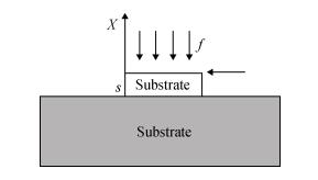
Fig. 1.
Schematic drawn of sample geometry used in film surface temperature calculation
SEMICONDUCTOR TECHNOLOGY
F. Khelfaoui1 and M. S. Aida2,
Corresponding author: M. S. Aida Email: aida_salah2@yahoo.fr
Abstract: A calculation of film surface temperature during thin films growth by sputtering technique is proposed. The calculation procedure is based on the conversion into heat of the total flux energy of species impinging the film surface during growth. The results indicate that the film's surface temperature depends drastically on material substrate thermal conductivity and thickness on one hand, and the plasma conditions namely the discharge power on the other. The predicted film surface temperatures were used to explain the microstructure evolution of hydrogenated amorphous silicon (a-Si:H) thin films deposited by reactive radio frequency (RF) sputtering on different substrates.
Keywords: sputtering deposition, plasma, amorphous silicon, thin films
| [1] |
Berish I R. Sputtering by particle bombardment. Berin: Springer Verlag, 1981
|
| [2] |
Matsuda A. Formation kinetics and control of microcrystallite in μc-Si:H from glow discharge plasma. J Non Cryst Solids, 1983, 59/60:767 doi: 10.1016/0022-3093(83)90284-3
|
| [3] |
Myers A M, Doyle J R, Feng G J, et al. Energetic particle fluxes in magnetron sputter deposition of A-Si:H. J Non Cryst Solids, 1991, 137/138:783 doi: 10.1016/S0022-3093(05)80237-6
|
| [4] |
Hopwood J. Ion bombardment energy distribution in a radio frequency plasma. Appl Phys Lett, 1993, 62(9):940 doi: 10.1063/1.108526
|
| [5] |
Kersten H, Stoffels E, Stoffels M M, et al. The energy balance at substrate surfaces during plasma processing. J Appl Phys, 2000, 87(8):3637 doi: 10.1063/1.372393
|
| [6] |
Edelberg E A, Aydil E S. Modeling of the sheath and the energy distribution of ions bombarding RF-biased substrates in high den-sity plasma reactors and comparison to experimental measurements. J Appl Phys, 1999, 86(9):4799 doi: 10.1063/1.371446
|
| [7] |
Drüsedau T P, Block T, John T M, et al. Energy transfer into the growing film during sputter deposition:an investigation by calorimetric measurements and Monte Carlo simulations. J Vac Sci Technol A, 1911, 15(5):2896 https://core.ac.uk/display/46008818
|
| [8] |
Aida M S, Mirouh K. Effect of RF power on the microstructure of a-Si:H films. Phys Stat Sol A, 1993, 136:K31 doi: 10.1002/(ISSN)1521-396X
|
| [9] |
Abdesselem S, Aida M S, Attaf N, et al. Growth mechanism of sputtered amorphous silicon thin films. Physica B, 2006, 373:331 http://www.sciencedirect.com/science/article/pii/S0921452605011932
|
| [10] |
Carlson D E, Wronski C R. Amorphous silicon solar cell. Appl Phys Lett, 1976, 28:671 doi: 10.1063/1.88617
|
| [11] |
Carlson D E. Recent developments in amorphous silicon solar cells. Sol Energy Mater, 1980, 3:503 doi: 10.1016/0165-1633(80)90002-7
|
| [12] |
Hamakawa Y, Okamoto H, Tawada T. Valency control of glow discharge produced a-SiC:H and its application to heterojunction solar cells. Int J Solar Energy, 1982, 1:125 doi: 10.1080/01425918208909880
|
| [13] |
LeComber P G, Spear E W, Gaith A. Amorphous silicon fieldeffect device and possible application. Electron Lett, 1989, 15:179 doi: 10.1049/el_19790126
|
| [14] |
LeComber P G, Spear W E. Semiconductors and semimetals. Orlando:Academic, 1984, 21:8
|
| [15] |
Lustig N, Kanicki J, Wisnieff R, et al. Temperature dependent characteristics of hydrogenated amorphous silicon thin film transistors. Mater Res Soc Symp Proc, 1988, 118:267 doi: 10.1557/PROC-118-267
|
| [16] |
Chittick R C, Alexander J H, Sterling H F. The preparation and properties of amorphous silicon. J Electrochem Soc, 1969, 77:116 doi: 10.1201/9780203911778.ch2
|
| [17] |
Spear W E, LeComber P G. Substitutional doping of amorphous silicon. Solid State Commun, 1975, 17:1193 doi: 10.1016/0038-1098(75)90284-7
|
| [18] |
Ross R C, Messier R. Microstructure and properties of RF sputtered amorphous hydrogenated silicon films. J Appl Phys, 1981, 52:5329 doi: 10.1063/1.329391
|
| [19] |
Freeman E C, Paul W. Optical constants of RF sputtered hydrogenated amorphous Si. Phys Rev B, 1979, 20:716 doi: 10.1103/PhysRevB.20.716
|
| [20] |
Abelson J R. Plasma deposition of hydrogenated amorphous silicon:studies of the growth surface. Appl Phys A, 1993, 56:493 doi: 10.1007/BF00331400
|
| [21] |
Aida M S, Rahmane S. Measurement of Ar ions striking force of the substrate during a-Si:H thin films sputtering deposition. Thin Solid films, 1996, 288:83 doi: 10.1016/S0040-6090(96)08822-0
|
| [22] |
Aida M S, Bachiri R. The surface properties of sputtered amorphous silicon thin films. J Non Cryst Solid, 1995, 189:167 doi: 10.1016/0022-3093(95)00196-4
|
| [23] |
McGahanWA.Solutions of the heat conduction equation in mul-tilayers for photothermal deflection experiments. J Appl Phys, 1992, 72(4):1362 doi: 10.1063/1.351747
|
| [24] |
Aida M S. Energy distribution of Ar ions at the substrate in the sputtering deposition of a-Si:H films. J Non Cryst Solids, 1993, 160:99 doi: 10.1016/0022-3093(93)90289-A
|
| [25] |
Benchiheb N, Aida M S, Attaf N. Plasma optical emission spectroscopy diagnostic during amorphous silicon thin films deposition by RF sputtering technique. Mater Sci Eng B, 2010, 172:191 doi: 10.1016/j.mseb.2010.05.018
|
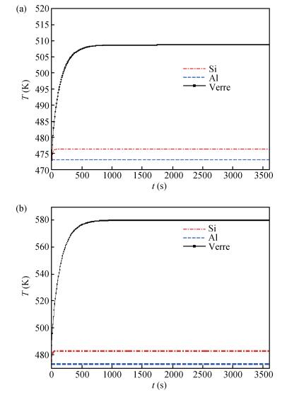
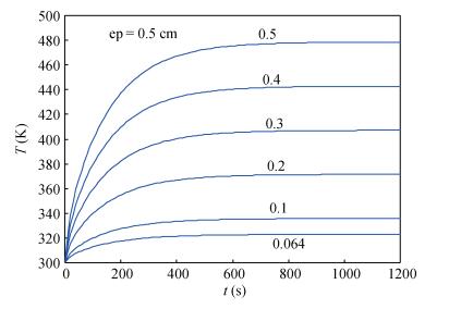

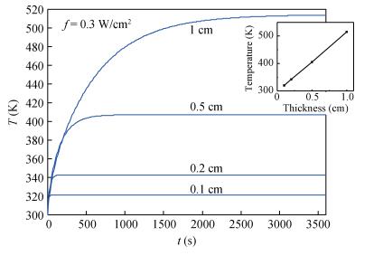
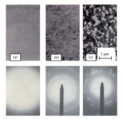
Table 1. Some physics properties of the used substrates[23]
 |
| [1] |
Berish I R. Sputtering by particle bombardment. Berin: Springer Verlag, 1981
|
| [2] |
Matsuda A. Formation kinetics and control of microcrystallite in μc-Si:H from glow discharge plasma. J Non Cryst Solids, 1983, 59/60:767 doi: 10.1016/0022-3093(83)90284-3
|
| [3] |
Myers A M, Doyle J R, Feng G J, et al. Energetic particle fluxes in magnetron sputter deposition of A-Si:H. J Non Cryst Solids, 1991, 137/138:783 doi: 10.1016/S0022-3093(05)80237-6
|
| [4] |
Hopwood J. Ion bombardment energy distribution in a radio frequency plasma. Appl Phys Lett, 1993, 62(9):940 doi: 10.1063/1.108526
|
| [5] |
Kersten H, Stoffels E, Stoffels M M, et al. The energy balance at substrate surfaces during plasma processing. J Appl Phys, 2000, 87(8):3637 doi: 10.1063/1.372393
|
| [6] |
Edelberg E A, Aydil E S. Modeling of the sheath and the energy distribution of ions bombarding RF-biased substrates in high den-sity plasma reactors and comparison to experimental measurements. J Appl Phys, 1999, 86(9):4799 doi: 10.1063/1.371446
|
| [7] |
Drüsedau T P, Block T, John T M, et al. Energy transfer into the growing film during sputter deposition:an investigation by calorimetric measurements and Monte Carlo simulations. J Vac Sci Technol A, 1911, 15(5):2896 https://core.ac.uk/display/46008818
|
| [8] |
Aida M S, Mirouh K. Effect of RF power on the microstructure of a-Si:H films. Phys Stat Sol A, 1993, 136:K31 doi: 10.1002/(ISSN)1521-396X
|
| [9] |
Abdesselem S, Aida M S, Attaf N, et al. Growth mechanism of sputtered amorphous silicon thin films. Physica B, 2006, 373:331 http://www.sciencedirect.com/science/article/pii/S0921452605011932
|
| [10] |
Carlson D E, Wronski C R. Amorphous silicon solar cell. Appl Phys Lett, 1976, 28:671 doi: 10.1063/1.88617
|
| [11] |
Carlson D E. Recent developments in amorphous silicon solar cells. Sol Energy Mater, 1980, 3:503 doi: 10.1016/0165-1633(80)90002-7
|
| [12] |
Hamakawa Y, Okamoto H, Tawada T. Valency control of glow discharge produced a-SiC:H and its application to heterojunction solar cells. Int J Solar Energy, 1982, 1:125 doi: 10.1080/01425918208909880
|
| [13] |
LeComber P G, Spear E W, Gaith A. Amorphous silicon fieldeffect device and possible application. Electron Lett, 1989, 15:179 doi: 10.1049/el_19790126
|
| [14] |
LeComber P G, Spear W E. Semiconductors and semimetals. Orlando:Academic, 1984, 21:8
|
| [15] |
Lustig N, Kanicki J, Wisnieff R, et al. Temperature dependent characteristics of hydrogenated amorphous silicon thin film transistors. Mater Res Soc Symp Proc, 1988, 118:267 doi: 10.1557/PROC-118-267
|
| [16] |
Chittick R C, Alexander J H, Sterling H F. The preparation and properties of amorphous silicon. J Electrochem Soc, 1969, 77:116 doi: 10.1201/9780203911778.ch2
|
| [17] |
Spear W E, LeComber P G. Substitutional doping of amorphous silicon. Solid State Commun, 1975, 17:1193 doi: 10.1016/0038-1098(75)90284-7
|
| [18] |
Ross R C, Messier R. Microstructure and properties of RF sputtered amorphous hydrogenated silicon films. J Appl Phys, 1981, 52:5329 doi: 10.1063/1.329391
|
| [19] |
Freeman E C, Paul W. Optical constants of RF sputtered hydrogenated amorphous Si. Phys Rev B, 1979, 20:716 doi: 10.1103/PhysRevB.20.716
|
| [20] |
Abelson J R. Plasma deposition of hydrogenated amorphous silicon:studies of the growth surface. Appl Phys A, 1993, 56:493 doi: 10.1007/BF00331400
|
| [21] |
Aida M S, Rahmane S. Measurement of Ar ions striking force of the substrate during a-Si:H thin films sputtering deposition. Thin Solid films, 1996, 288:83 doi: 10.1016/S0040-6090(96)08822-0
|
| [22] |
Aida M S, Bachiri R. The surface properties of sputtered amorphous silicon thin films. J Non Cryst Solid, 1995, 189:167 doi: 10.1016/0022-3093(95)00196-4
|
| [23] |
McGahanWA.Solutions of the heat conduction equation in mul-tilayers for photothermal deflection experiments. J Appl Phys, 1992, 72(4):1362 doi: 10.1063/1.351747
|
| [24] |
Aida M S. Energy distribution of Ar ions at the substrate in the sputtering deposition of a-Si:H films. J Non Cryst Solids, 1993, 160:99 doi: 10.1016/0022-3093(93)90289-A
|
| [25] |
Benchiheb N, Aida M S, Attaf N. Plasma optical emission spectroscopy diagnostic during amorphous silicon thin films deposition by RF sputtering technique. Mater Sci Eng B, 2010, 172:191 doi: 10.1016/j.mseb.2010.05.018
|


Article views: 4346 Times PDF downloads: 45 Times Cited by: 0 Times
Received: 13 July 2016 Revised: 26 February 2017 Online: Published: 01 September 2017
| Citation: |
F. Khelfaoui, M. S. Aida. Films surface temperature calculation during growth by sputtering technique[J]. Journal of Semiconductors, 2017, 38(9): 096001. doi: 10.1088/1674-4926/38/9/096001
****
F. Khelfaoui, M. S. Aida. Films surface temperature calculation during growth by sputtering technique[J]. J. Semicond., 2017, 38(9): 096001. doi: 10.1088/1674-4926/38/9/096001.

|
| [1] |
Berish I R. Sputtering by particle bombardment. Berin: Springer Verlag, 1981
|
| [2] |
Matsuda A. Formation kinetics and control of microcrystallite in μc-Si:H from glow discharge plasma. J Non Cryst Solids, 1983, 59/60:767 doi: 10.1016/0022-3093(83)90284-3
|
| [3] |
Myers A M, Doyle J R, Feng G J, et al. Energetic particle fluxes in magnetron sputter deposition of A-Si:H. J Non Cryst Solids, 1991, 137/138:783 doi: 10.1016/S0022-3093(05)80237-6
|
| [4] |
Hopwood J. Ion bombardment energy distribution in a radio frequency plasma. Appl Phys Lett, 1993, 62(9):940 doi: 10.1063/1.108526
|
| [5] |
Kersten H, Stoffels E, Stoffels M M, et al. The energy balance at substrate surfaces during plasma processing. J Appl Phys, 2000, 87(8):3637 doi: 10.1063/1.372393
|
| [6] |
Edelberg E A, Aydil E S. Modeling of the sheath and the energy distribution of ions bombarding RF-biased substrates in high den-sity plasma reactors and comparison to experimental measurements. J Appl Phys, 1999, 86(9):4799 doi: 10.1063/1.371446
|
| [7] |
Drüsedau T P, Block T, John T M, et al. Energy transfer into the growing film during sputter deposition:an investigation by calorimetric measurements and Monte Carlo simulations. J Vac Sci Technol A, 1911, 15(5):2896 https://core.ac.uk/display/46008818
|
| [8] |
Aida M S, Mirouh K. Effect of RF power on the microstructure of a-Si:H films. Phys Stat Sol A, 1993, 136:K31 doi: 10.1002/(ISSN)1521-396X
|
| [9] |
Abdesselem S, Aida M S, Attaf N, et al. Growth mechanism of sputtered amorphous silicon thin films. Physica B, 2006, 373:331 http://www.sciencedirect.com/science/article/pii/S0921452605011932
|
| [10] |
Carlson D E, Wronski C R. Amorphous silicon solar cell. Appl Phys Lett, 1976, 28:671 doi: 10.1063/1.88617
|
| [11] |
Carlson D E. Recent developments in amorphous silicon solar cells. Sol Energy Mater, 1980, 3:503 doi: 10.1016/0165-1633(80)90002-7
|
| [12] |
Hamakawa Y, Okamoto H, Tawada T. Valency control of glow discharge produced a-SiC:H and its application to heterojunction solar cells. Int J Solar Energy, 1982, 1:125 doi: 10.1080/01425918208909880
|
| [13] |
LeComber P G, Spear E W, Gaith A. Amorphous silicon fieldeffect device and possible application. Electron Lett, 1989, 15:179 doi: 10.1049/el_19790126
|
| [14] |
LeComber P G, Spear W E. Semiconductors and semimetals. Orlando:Academic, 1984, 21:8
|
| [15] |
Lustig N, Kanicki J, Wisnieff R, et al. Temperature dependent characteristics of hydrogenated amorphous silicon thin film transistors. Mater Res Soc Symp Proc, 1988, 118:267 doi: 10.1557/PROC-118-267
|
| [16] |
Chittick R C, Alexander J H, Sterling H F. The preparation and properties of amorphous silicon. J Electrochem Soc, 1969, 77:116 doi: 10.1201/9780203911778.ch2
|
| [17] |
Spear W E, LeComber P G. Substitutional doping of amorphous silicon. Solid State Commun, 1975, 17:1193 doi: 10.1016/0038-1098(75)90284-7
|
| [18] |
Ross R C, Messier R. Microstructure and properties of RF sputtered amorphous hydrogenated silicon films. J Appl Phys, 1981, 52:5329 doi: 10.1063/1.329391
|
| [19] |
Freeman E C, Paul W. Optical constants of RF sputtered hydrogenated amorphous Si. Phys Rev B, 1979, 20:716 doi: 10.1103/PhysRevB.20.716
|
| [20] |
Abelson J R. Plasma deposition of hydrogenated amorphous silicon:studies of the growth surface. Appl Phys A, 1993, 56:493 doi: 10.1007/BF00331400
|
| [21] |
Aida M S, Rahmane S. Measurement of Ar ions striking force of the substrate during a-Si:H thin films sputtering deposition. Thin Solid films, 1996, 288:83 doi: 10.1016/S0040-6090(96)08822-0
|
| [22] |
Aida M S, Bachiri R. The surface properties of sputtered amorphous silicon thin films. J Non Cryst Solid, 1995, 189:167 doi: 10.1016/0022-3093(95)00196-4
|
| [23] |
McGahanWA.Solutions of the heat conduction equation in mul-tilayers for photothermal deflection experiments. J Appl Phys, 1992, 72(4):1362 doi: 10.1063/1.351747
|
| [24] |
Aida M S. Energy distribution of Ar ions at the substrate in the sputtering deposition of a-Si:H films. J Non Cryst Solids, 1993, 160:99 doi: 10.1016/0022-3093(93)90289-A
|
| [25] |
Benchiheb N, Aida M S, Attaf N. Plasma optical emission spectroscopy diagnostic during amorphous silicon thin films deposition by RF sputtering technique. Mater Sci Eng B, 2010, 172:191 doi: 10.1016/j.mseb.2010.05.018
|

 WeChat ID
Journal of Semiconductors © 2017 All Rights Reserved 京ICP备05085259号-2

 DownLoad:

