Processing math: 100%
J. Semicond. > 2018, Volume 39 > Issue 10 > 101001

INVITED REVIEW PAPERS

InP-based monolithically integrated few-mode devices

Dan Lu1, 2, 3, , Yiming He1, 2, 3, Zhaosong Li1, 2, 3, Lingjuan Zhao1, 2, 3 and Wei Wang1, 2, 3

+ Author Affiliations

 Corresponding author: Dan Lu, Email: ludan@semi.ac.cn

DOI: 10.1088/1674-4926/39/10/101001

PDF

Turn off MathJax

Abstract: Mode-division multiplexing (MDM) has become an increasingly important technology to further increase the transmission capacity of both optical-fiber-based communication networks, data centers and waveguide-based on-chip optical interconnects. Mode manipulation devices are indispensable in MDM system and have been widely studied in fiber, planar lightwave circuits, and silicon and InP based platforms. InP-based integration technology provides the easiest accessibility to bring together the functions of laser sources, modulators, and mode manipulation devices into a single chip, making it a promising solution for fully integrated few-mode transmitters in the MDM system. This paper reviews the recent progress in InP-based mode manipulation devices, including the few-mode converters, multiplexers, demultiplexers, and transmitters. The working principle, structures, and performance of InP-based few-mode devices are discussed.

Key words: mode division multiplexingmode convertermode multiplexerfew mode transmittersphotonics integrated circuit

Space-division multiplexing (SDM) and mode-division multiplexing (MDM) technologies are now gaining popularity among both the academia and the industry. Fiber modes or waveguide modes are used as another degree of freedom in addition to the traditional multiplexing technologies to increase the transmission capacity of communication networks or on-chip systems. Due to a large number of available spatial and mode channels, the spectral efficiency of the experimental optical transmission system has been increased to a record level of 1000 bit/s/Hz[1] with the aid of SDM/MDM technology, two orders of magnitude higher than that of the single-mode channel. The future deployment of SDM/MDM technology in long-distance telecom will be a viable solution with the maturation of few-mode devices such as few-mode transceivers, amplifiers, routers, etc. In cost-insensitive long-distance applications, the few-mode devices can be manufactured in many material platforms, including III/V, Si, glass, lithium-niobate, etc. While for short-reach application, such as datacom and on-chip interconnects, the vast number of communication channels and access points place considerable pressure on components cost. Cost-effective and technologically-simpler solutions are more preferred when introducing new technologies to short-reach applications in addition to the currently adopted wavelength division multiplexing (WDM) and multilevel coding (such as PAM-4) technologies. On-chip SDM/MDM technologies in III/V or Si platforms provide a promising solution, which can be attributed to the channel characteristics of short-range applications and the volume-production characteristic of the semiconductor industry. For systems, in short-reach applications, especially the on-chip systems, the influences of dispersion, polarization perturbations, and intermodal interference are much less than that of the long-distance system, significantly reducing the need for complex multiple-input-multiple-output (MIMO) digital signal processing (DSP). The demodulation and detection of signals from SDM/MDM channels can be much simpler and cheaper than that of the long-distance network. Simple intensity-modulation direct-detection (IM/DD) technology can still be used in short-reach datacom and on-chip systems after introducing the SDM/MDM technology. For devices, only the semiconductor integration platforms can meet the demands for large volume, low-cost production of functional few-mode devices in SDM/MDM systems, especially the few-mode converters/multiplexers/demultiplexers (C/M/D) and transmitters.

Silicon photonics and InP photonics are two major material systems for few-mode devices. Silicon photonics provides a high-level of flexibility and processing maturity for complex and large-scale integrated passive few-mode C/M/D[28]. However, the difficulty in efficient lasing and amplification in the silicon platform remain as a problem for a silicon-based fully integrated few-mode transmitter. While the InP platform, with the advantage in the active and passive components integration, can offer the integration possibility of not only the passive few-mode C/M/Ds[916] but also the lasers and amplifiers with the passive few-mode components. Fully functional integrated few-mode transmitters can be readily fabricated based on current technology[17]. It is a promising solution to considerably reduce the complexity, footprint, power consumption and cost of short-reach applications.

Silicon-based few-mode devices have been widely studied and reviewed[18], but there is still no systematic review on the InP-based few-mode devices. The differences in material platforms, design considerations, structures, performance and applications in the two-material system still necessitate an overview of the InP-based few-mode devices. In this paper, we will review the recent progress in InP-based few-mode devices, including few-mode converters, multiplexers, demultiplexers, and transmitters. The working principle, structures, and performance of the InP-based few-mode devices are discussed.

Modes generation, conversion, multiplexing, and demultiplexing are indispensable to an MDM system. Fig. 1 shows the typical configurations of a few-mode transmitter and a few-mode receiver. The few-mode transmitter usually consists of one or several laser sources, modulators, mode converters, and mode multiplexers. The laser sources are normally single (transverse) mode lasers, serving as optical carriers. The modulators can be either external modulators (e.g., Mach–Zehnder modulators or electronic-absorption modulators) or directly modulated lasers (DML). If a directly modulated laser is used, it can be viewed as a multifunctional device, capable of generating optical carrier and being modulated. The modulators transfer the information into different mode (to be converted) channels. The mode converters convert the single (transverse) modes into desired higher-order (transverse) modes. The mode multiplexers combine all mode channels into a single channel, ready for transmission into few-mode fibers or waveguides. To demodulate the signal at the receiver, the multiplexed modes should be first demultiplexed into different channels and then converted into a single mode, and finally detected by the photodetectors in each channel. In the receiver, mode conversion is optional if the photodetectors are accessed by multimode waveguides or fibers, i.e., no mode conversion is needed in the case of direct detecting higher-order modes.

Figure  1.  (Color online) Schematic configuration of (a) a few-mode transmitter and (b) a few-mode receiver.

Many types of mode C/M/D have been demonstrated in both silicon and InP platforms. Typical structures include asymmetrical directional couplers (ADC)[4, 19], tapered-waveguide structures[20, 21], multimode interference (MMI) couplers[914], Y–junctions[2225], etc. Fig. 2(a) shows a schematic ADC mode converter where a single-mode access waveguide and a multimode bus waveguide are coupled through an evanescent coupling region. By properly choosing the waveguide width, gap width, and coupling-region length, efficient mode conversion can be realized for modes with the same effective refractive indices, e.g., the fundamental mode in the narrower single mode waveguide and the first-order mode in the wider multimode waveguide. For modes with different effective refractive indices, mode coupling is very weak. Thus, mode conversion between desired modes can be realized with low crosstalk. Fig. 2(b) shows a tapered-waveguide-based mode converter, where a single-mode waveguide and a multimode waveguide are connected by an adiabatic tapered waveguide. Mode conversion is realized in the adiabatic taper due to mode hybridization[18]. The mode hybridization usually happens at some specific waveguide width (wh) where some eigenmodes of specific orders (e.g., TM0, TE1) are indistinguishable. If the end width of the taper (w1, w2) satisfies w1 < wh < w2, efficient mode conversion will be achieved after the launched optical mode propagates through the taper. ADC and tapered-structure based mode converters usually require precise control of the coupling gap, waveguide width on a submicron level. The two structures are mostly reported in silicon platforms but rarely realized in the InP platform due to the difference in processing the precision control level.

Figure  2.  (Color online) Mode converters using (a) asymmetrical directional couplers and (b) tapered structure.

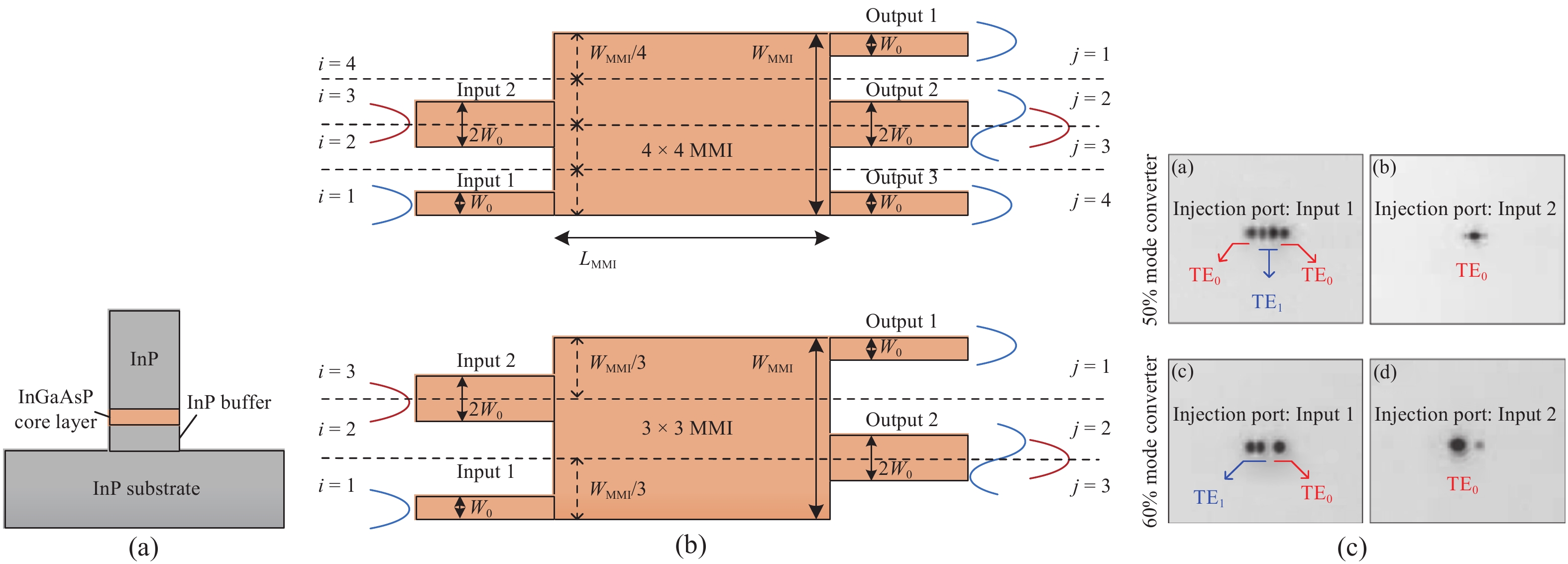
In the InP platform, MMI and Y-junctions are two major structures for mode converters. The MMI-based mode converters can normally realize mode conversion between the fundamental TE0 mode and the first-order TE1 mode. When an MMI is used as a TE0 –> TE1 mode converter, the MMI should be a general-MMI. The input arm (width w0) should be placed at the MMI edge, and the output arm needs to be a merged waveguide (width w1 = 2w0) of two adjacent output ports, as shown in Fig. 3(a). The basic idea is to combine two images of the input TE0 mode into the form of TE1 mode at the output waveguide. Two factors have to be taken into consideration[9].

Figure  3.  (Color online) Mode converters using (a) a 3 × 3 MMI as a 66%-MMI-converter and (b) a 1 × 2 MMI and a 4 × 4 MMI as a 100%-MMI-converter (Ref. [9]).

1) The position of the input waveguide should be chosen so that two adjacent output waveguides of the MMI touch each other to form a wider waveguide supporting a first-order mode. At the same time, the portion of energy distributed in the two adjacent output waveguides should be equal to guarantee an optimum excitation of the first-order mode. The condition will be satisfied for an N × N general-MMI with a position parameter being half of the rib width, as shown in Fig. 3(a).

2) Secondly, the phase relationship between the output fields at the two adjacent waveguides should be out-of-phase, so that the combined field has the same phase distribution as that of a first-order mode. For an N × N general-MMI, if the optical mode is launched at the first input port with port number i = 1,a phase-shift of π will be obtained between the output ports with port number j = 2m and j = 2m + 1, with m being an integer in the range of [1, N – 1][26]. For example, the output port 2 and 3 will be out of phase for a 3 × 3 MMI and a 4 × 4 MMI when the light is launched at input port 1, as shown in Figs. 3(a) and 3(b).

3 × 3 MMI
N = 3 j = 1 j = 2 j = 3
i = 1 −3π/3 −2π/3 −5π/3
i = 2 −2π/3 −3π/3 −2π/3
i = 3 −5π/3 −2π/3 −3π/3
DownLoad: CSV  | Show Table
4 × 4 MMI
N = 4 j = 1 j = 2 j = 3 j = 4
i = 1 −4π/4 −3π/4 −7π/4 −4π/4
i = 2 −3π/4 −4π/4 −4π/4 −7π/4
i = 3 −7π/4 −4π/4 −4π/4 −3π/4
i = 4 −4π/4 −7π/4 −3π/4 −4π/4
DownLoad: CSV  | Show Table

The phase relationship Δφij between the input and output ports for a general N × N MMIs can be summarized as Eq. (1)[9]:

i+jeven:Δϕij=ϕ0ππ4N(ji)(2Nj+i),i+jodd:Δϕij=ϕ0π4N(j+i1)(2Nji+1),
(1)

where φ0 is a constant phase shift depending on the MMI length. The phase relationships for a general 2 × 2 MMI, 3 × 3 MMI and 4 × 4 MMI are listed in Table 1 for reference.

Table  1.  Phase-relations of the general 2 × 2 MMI, 3 × 3 MMI and 4 × 4 MMI. i is the input port number, and j is the output port number.
2 × 2 MMI
N = 2 j = 1 j = 2
i = 1 −2π/2 −π/2
i = 2 −π/2 −2π/2
DownLoad: CSV  | Show Table

For a mode converter using a 3 × 3 MMI, the output first-order mode contains 66% of the input energy from input port 1. It is usually referred to as a 66%-MMI-converter. Similarly, a structure using a 4 × 4 MMI is called a 50%-MMI-converter. To realize a mode converter with 100% conversion efficiency, a more sophisticated structure should be adopted, as shown in Fig. 3(b). It consists of a symmetric 1 × 2 MMI as the optical splitter, a 4 × 4 MMI as the mode converter. A π-phase-shifter is introduced into one of the output arms of the 1 × 2 MMI so that the outputs at the port 1 and 4 of the 4 × 4 MMI cancel each other, while the outputs at port 2 and 3 interfere constructively.

The MMI-based mode converters can be further used as mode-converter-multiplexers. By placing another input waveguide at an appropriate position as the fundamental mode channel in conjunction with the previously described first-order mode channel, it is possible to obtain a multiplexed output combining the fundamental mode and the first-order mode at the same output port. For a 66%-MMI-converter-multiplexer, as shown in Fig. 4(a) the fundamental mode channel A should be placed at Weq/3 from the top of the MMI if the first-order mode channel B is placed at the bottom, where Weq is the width of the MMI. For a 100%-MMI-converter-multiplexer, an extra access waveguide can be introduced at Weq/2 of the 50%-MMI-converter as the fundamental mode channel. However, such an access waveguide will result in a waveguide crossing in-between the 1 × 2 MMI and 4 × 4 MMI. An alternative solution is to replace the 1 × 2 MMI with a 2 × 2 MMI. The fundamental-mode channel is placed at Weq/2 of the 2 × 2 MMI, and the first-order-mode channel is placed at the edge. Considering there is already a π/2 phase-shift between the upper and lower input arms of the 50%-MMI-converter, only an extra π/2-phase-shifter is needed. The mode-converter-multiplexers can also be used as mode converter-demultiplexers by simply reversing the input and output ports.

Figure  4.  (Color online) Mode converter-multiplexers with mode conversion of (a) 66% and (b) 100% (Ref. [9]).

Y-junctions are also widely used as mode C/M/Ds. The symmetrical Y-junction consists of two single-mode branching waveguides and a multimode stem waveguide, as shown in Fig. 5(a). When two in-phase modes are launched from the single-mode arms, they will excite an even mode at the junction, and evolve into the fundamental mode in the multimode waveguide[27]. When two out-of-phase modes are launched, they will excite an odd mode at the junction, and evolve into the first-order mode in the multimode waveguide. When two sets of in-phase and out-of-phase modes are launched simultaneously, mode conversion and multiplexing are realized. Asymmetrical Y-junctions are usually used as a mode converter-demultiplexer. For an asymmetrical Y-junction as shown in Fig. 5(b), when a fundamental mode is launched from the stem multimode waveguide, it will exit from the wider branching arm as a fundamental mode due to the matching of effective modal indices between the stem and the wider waveguide. When a first-order mode is launched from the stem waveguide, it will exit from the narrower branching arm as a fundamental mode since the effective modal index of the first-order mode matches that of the narrower waveguide[24].

Figure  5.  (Color online) (a) Mode converters-multiplexer using symmetrical Y-junction and (b) mode converter-demultiplexer using asymmetrical Y-junction.

In the following section, we will review several typical InP-based few-mode converters, multiplexers, and demultiplexers based on their structure, including single-MMI-based, cascaded-MMI-based, MMI-Y-junction-based, and reconfigurable mode C/M/Ds. Finally, a fully-integrated few-mode transmitter is discussed.

The basic working principles of mode manipulation structures have been well established in the 1980’s and 1990’s. In the 1990’s both Y-junction-based[28] and MMI-based mode converters[9] have been demonstrated to realize polarization splitter, all-optical switches, and wavelength-converters. The main functions of higher-order modes were intended for control instead of as information channels. The real functional devices aiming at MDM only appear recently with the development of MDM technology in both telecom, on-chip interconnects, and datacom. As mentioned in the introduction, most integrated mode manipulation devices are still passive, using silicon as the material platform. Silicon-based few-mode components can be further integrated to a large scale level to perform more complexed functions. It is suitable for telecom requiring the combination of several multiplexing methods, including WDM, PDM (polarization division multiplexing), MDM, etc. as well as higher-order modulation format. However, for datacom and short-reach applications, a low-cost solution with simple structures is highly preferred. The InP platform provides an excellent option for such applications due to its capability to integrate lasers, modulators, and mode C/M/Ds.

In 2016, we revisited Leuthold’s scheme using MMI as a few-mode C/M/D[9]. The purpose was to verify their characteristics of broadband operation and higher-order fiber-modes excitation. MMI-based mode converters working in the O-band[11] and C-band[12] were realized and demonstrated. Fig. 6(a) shows the epitaxial structure of the O-band mode-converter. It consisted of a 500-nm InP buffer, a 300-nm InGaAsP core layer with a 1.15-μm bandgap, and a 1.7-μm InP cladding layer. Fig. 6(b) shows the schematic structures of the 50%- and 66%-MMI-converter. The two devices were fabricated with a length of 371 and 495 μm, respectively. Mode conversion from TE0 to TE1 was successfully demonstrated in the wavelength range of 1280–1320 nm. Fig. 6(c) shows the mode pattern obtained from the manufactured 50%- and 66%-MMI-converter. Similar results were also obtained for mode converters in the wavelength range from 1520–1565 nm. The generated TE0 to TE1 were coupled into a two-mode fiber, LP01 and LP11 modes were successfully excited. Table 2 shows the first-order TE1 modes from a 66%-MMI-converter and LP11 modes excited by the TE1 modes at various wavelengths.

Figure  6.  (Color online) (a) Epitaxial structure of the MMI-based mode converters, (b) schematic structures, and (c) the experimentally observed mode patterns corresponding to 50%- and 66%-MMI-converter (Ref. [11]).
Table  2.  The waveguide TE1 modes obtained from a 66%-MMI-converter and the excited fiber LP11 modes at various wavelengths in the C-band (Ref. [12]).
1520 nm 1540 nm 1550 nm 1565 nm
Waveguide mode TE1
Fiber mode LP11
DownLoad: CSV  | Show Table

For the MMI-based mode converters/multiplexers, the operational mode order is typically limited to two modes. To realize higher-order mode conversion, additional structure can be introduced. By using a modified 3 × 3 MMI and an enlarged butterfly-shaped phase shifter, a mode converter capable of converting TE0 to TE2 has been demonstrated in SOI platform[8], which can also be applied to the InP platform to further scale the mode conversion order.

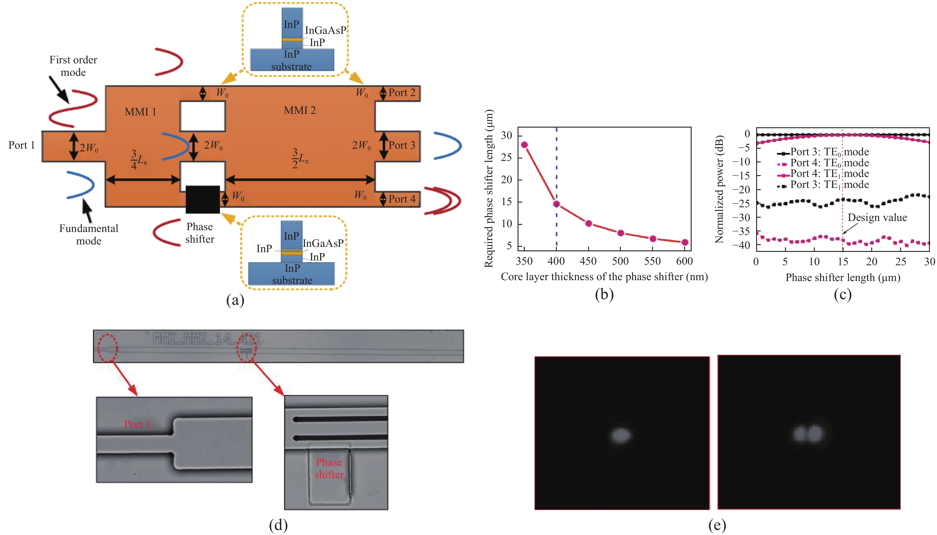
To realize a 100%-MMI-C/M/D as shown in Fig. 3(b) or Fig. 4(b), a phase-shifter (PS) is required. The phase-shifter can be realized through bent waveguides with different radius[9], butterfly-shaped tapered structure[3] or tilted-joint connection[29]. However, these schemes will either result in a long PS section or a strict fabrication tolerance; care should also be taken to minimize the loss. To achieve more precise control and increase the processing tolerance, we proposed a PS structure with a thickness-detuned core layer[10], as shown in Fig. 7(a). By tuning the core-layer thickness of the PS section, the phase difference between the upper and lower input arms of MMI2 can be controlled precisely since the thickness error of the epitaxial layers is only a few nanometers, resulting in a precise control of the effective refractive index difference (Δn) between the PS arm and the other waveguide arm. Δn in this scheme will be on the order of ~10−2. Considering the phase difference of Δφ = 2π/λnL), where λ is the wavelength, L is the PS length, to achieve a π/2 phase shift, L will be on the order of 3–25λ, which is an appropriate length for InP processing control while still maintaining a small PS size. On the other hand, Δn will be small enough to make the structure rather insensitive to the PS length and increase the fabrication tolerance. Fig. 7(b) shows the calculated shortest π/2-PS length when changing the core-layer thickness of the PS section. During the simulation, the core layer of other waveguides was fixed at 300 nm. Taking into account the growth quality of epitaxial materials, a core layer thickness of 400 nm for the PS section was selected, with the corresponding PS section length being 14.7 μm. The epitaxial structure of the 100%-MMI-converter-multiplexer was similar to that shown in Fig. 6(a), with the exception that the core layer of the PS section was 100-nm thicker than that of other waveguides. The influence of the PS length on the insertion loss is shown in Fig. 7(c). Within ±8 μm from the selected PS length of 14.7 μm, the simulated insertion losses are lower than 1 dB for both the TE0 mode and TE1 mode. The crosstalk of the TE0 mode and the TE1 mode are below −21.8 and −36.3 dB, respectively. Fig. 7(d) shows the scanning electron microscopy (SEM) image of the fabricated device. In the enlarged inset, a visible elevated region can be found in the PS section due to the thicker core layer. The device was tested as a mode-converter by injecting a fundamental mode into Port3 and Port4, respectively. TE0 and TE1 modes were successfully obtained, as shown in Fig. 7(e). Broadband operation from 1520 to 1600 nm was also realized.

Besides using a thickness-detuned core layer to achieve the π/2 phase shift, a 1 × 1 MMI can also be used as a phase shifter[14]. The main advantage of using an MMI as the PS is that the whole device will be solely based on MMI couplers, which have been standardized as the building block in the generic foundry platform for the photonic integrated circuits[30]. This will make it compatible with standard manufacture processes for integration with other standard devices on InP substrate to form more advanced circuits. Another advantage is that by introducing the 1 × 1 MMI-PS, the upper and lower connecting arms between MMI 1 and MMI 2, as shown in Fig. 8(a), can adopt a simple straight waveguide of the same length, without the need to use bent or butterfly structures. The 1 × 1 MMI-PS will introduce a fixed phase shift of π, regardless of its length, while the phase delay of a straight waveguide increases linearly as its length. By adjusting the width and thereby the length of the 1 × 1 MMI, it is possible to obtain a phase difference of π/2 between the upper and lower arms. Fig. 8(b) shows the simulated field distribution of the 100%-MMI-converter-multiplexer based on an MMI-PS. In the design, the 1 × 1 MMI was 87 μm in length. In comparison, if a bent-waveguide were to be adopted, the length of the phase-shifter would be 200 μm with the curve radius of 1000 μm. Fig. 8(c) shows the TE0 and TE1 mode pattern from a fabricated device using this scheme.

Figure  8.  (Color online) A 100%-MMI-converter-multiplexer based on a 1 × 1 MMI phase-shifter. (a) The schematic device structure, (b) the simulated field distribution, and (c) the mode patterns (Ref. [14]).

The 100%-MMI C/M/D using a 4 × 4 MMI as the mode converters as shown in Fig. 7(a) and Fig. 8(a) require three connecting arms between the two MMIs. The MMIs are usually designed to be wide enough to avoid crosstalk between adjacent connecting arms. The increase of MMI width will cause a dramatic increase in the length of MMI when considering the quadratic relation of MMI’s length with width. The total lengths of the 100%-MMI-C/M/D above mentioned were all longer than 1 mm. An MMI-Y-junction structure was then proposed to realize a miniature 100%-mode-C/M/D[25]. It consisted of a 2 × 2 MMI coupler, a symmetric Y-junction, and a phase shifter with a thickness-detuned core layer, as shown in Fig. 9(a). For a general 2 × 2 MMI coupler, when a TE0 mode is launched from Port 1, it will be split into two beams of the same amplitude but a phase shift of −π/2 between Port 4 and Port 3. While for the TE0 mode launched from Port 2, the phase shift will be π/2. After passing through a π/2 phase-shifter, the two beams from Port 1 will be in-phase, and the beams from Port 2 will be out-of-phase. The in-phase and out-of-phase TE0 modes will be guided out of Port 5 as the TE0 and TE1 mode respectively. The simulated field distribution is shown in Fig. 9(b). The modes pattern from a fabricated device is shown in Fig. 9(c). Due to the reduction of connecting arms, the device size has been reduced to less than 500 nm, much shorter than other 100%-mode-C/M/D structures in InP materials.

Figure  9.  (Color online) A 100%-MMI-converter-multiplexer based on MMI-Y-junction. (a) The schematic device structure, (b) the simulated field distribution, and (c) the mode patterns. (Ref. [25]).
Figure  7.  (Color online) A 100%-MMI-converter-multiplexer scheme based on a core-thickness-detuned phase-shifter. (a) The schematic device structure, (b) the simulated phase shift versus the core layer thickness of the PS when the thicknesses of other waveguides are fixed at 300 nm, (c) the simulated influence of PS length on the insertion loss, (d) SEM images of the fabricated device, and (e) the mode patterns (Ref. [10]).

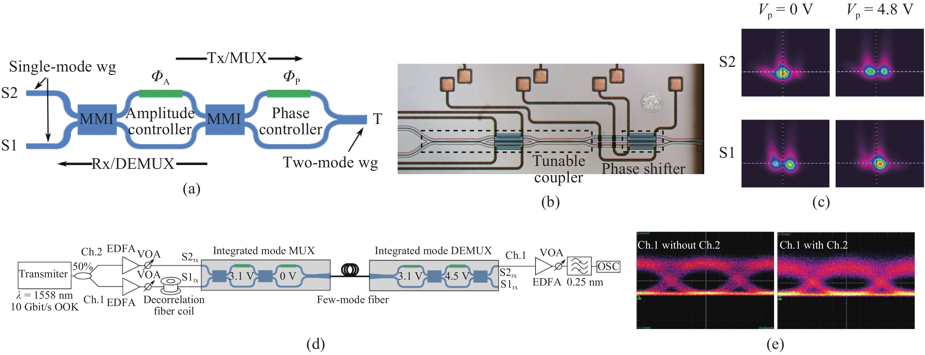
A reconfigurable photonic integrated mode C/M/D was proposed and demonstrated by Polytechnic University of Milan in 2016[16]. The schematic device structure is shown in Fig. 10(a). The mode C/M/D was realized using an MMI-based balanced Mach-Zehnder interferometer (MZI) and a symmetric Y-junction. Two thermally tunable phase sections were introduced in one arm of the Mach-Zehnder interferometer (amplitude controller) and one arm (phase controller) of the Y-junction, corresponding to a phase shift of φA and φP, respectively. The MZI was biased as a 3-dB coupler with φA being π/2 or 3π/2. The phase difference between the two output branches of the MZI will be either a (π, 0) or (0, π) pair depending on φA if two fundamental modes are simultaneously launched at S1 and S2. φP can be chosen to be 0 or π to control which input channel (S1 or S2) shall be converted to the TE1 mode. The structure is completely reconfigurable, and the two single-mode inputs can be mapped into any combination of the two modes of the output waveguide. The device was designed and fabricated on an InP-based generic technological platform through a Multi-Project Wafer run[30]. The device picture is shown in Fig. 10(b). The phase control at the amplitude controller and the phase controller are realized by applying a control voltage of VA and Vp respectively. The functionality of the mode C/M was tested by coupling a single mode laser through either S1 or S2, with a fixed MZI phase control of φA = π/2 (VA = 3.1 V). Fig. 10(c) shows the mode patterns corresponding to φP = 0 (VP = 0 V) and φP = π, (VP = 4.8 V) respectively. Switchable mode conversion can be observed. Since the circuit is completely balanced the operational bandwidth of the mode C/M is extremely wide. Operation wavelength at 1480 and 1550 nm were both demonstrated at the same control voltages. A transmission experiment was further carried out by using the chip as the mode C/M in the transmitter and as mode C/D at the receiver, as shown in Fig. 10(d). SDM transmission in a 2-meter few-mode fiber was demonstrated. Fig. 10(e) shows the DEMUXed eye diagram of one channel and two channels. Clear opened eye with Q-factor of 5.7 (single channel transmission) and 3.8 (double channel transmission) were demonstrated.

Figure  10.  (Color online) Reconfigurable mode C/M/D. (a) The schematic device structure, (b) the device picture, (c) the mode patterns corresponding to different phase controller voltage, (d) MDM transmission setup, and (e) the obtained eye diagram (Ref. [16]).

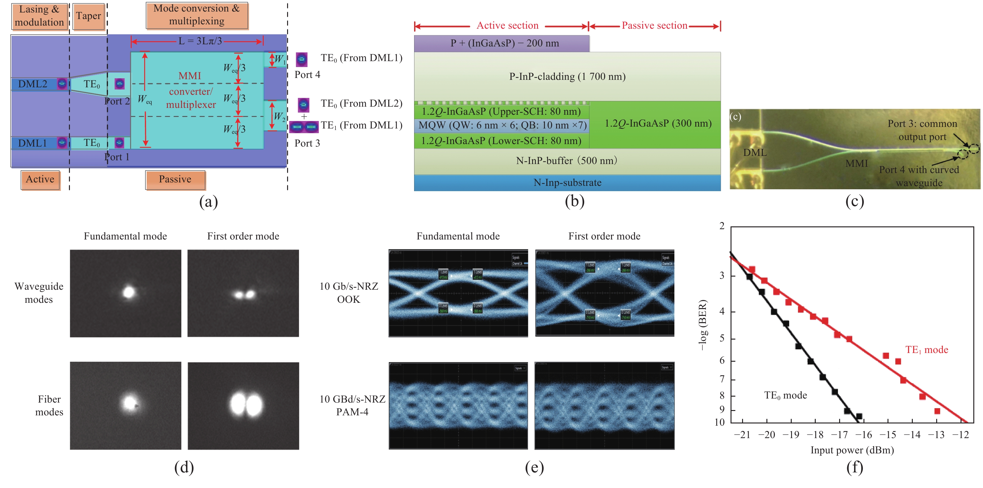
In 2018,we demonstrated a fully-integrated InP-based few-mode transmitter[17]. The transmitter consists of two directly modulated lasers (DMLs) and a 66%-MMI mode converter/multiplexer. The schematic structure of the few-mode transmitter is shown in Fig. 11(a). The two DMLs are distributed feedback lasers (DFB), responsible for generating two directly modulated TE0 modes. The MMI-based mode converter/multiplexer converts the TE0 mode from DML1 to TE1 mode and multiplexes the TE1 mode with the TE0 mode from DML2 at Port3 of the MMI. The epitaxial structure of the device is shown in Fig. 11(b). The active section is a multiple-quantum-well (MQW) structure with photoluminescence (PL) wavelength of 1.5 μm. The passive section has a 0.3-μm core layer with PL wavelength of 1.2 μm. The passive and active section was integrated using butt-joint technology. Fig. 11(c) shows a picture of the fabricated device. To avoid the influence of the unused Port4, a curved waveguide was designed to guide the unused TE0 mode power off the testing path. Fig. 11(d) shows the TE0 mode and TE1 mode patterns generated from the few-mode transmitter and the fundamental fiber LP01 and first-order fiber LP11 mode excited by the waveguide modes, respectively. The transmitter works at a wavelength around 1538 nm, with the side mode suppression ratios (SMSR) above 35 dB and −3 dB small-signal modulation bandwidth above 14 GHz. Direct modulation of the transmitter using 10-Gb/s non-return-to-zero (NRZ) on-off-key (OOK) signal and 10-Gbaud/s-NRZ 4-level pulse amplitude modulation (PAM-4) signal was demonstrated. Fig. 11(e) shows the eye-diagram of the 10-Gb/s-NRZ-OOK and 10 Gbaud/s-NRZ-PAM-4 signals corresponding to the fundamental mode and the first-order mode, respectively. Error-free receiving of the two-mode channels were also obtained in a 10 Gb/s-NRZ-OOK back-to-back bit error rate (BER) test. The power penalty between TE0 mode and TE1 mode was 4.3 dB at the BER of 10−9, as shown in Fig. 11(f). The directly modulated monolithic integrated few-mode transmitter may find potential applications in short-reach or on-chip MDM systems, where intensity modulation with direct detection (IM/DD) is preferred.

Figure  11.  (Color online)(a) The schematic device structure, (b) the epitaxial structure, (c) the device picture, (d) the waveguide modes and the excited fiber modes, (e) the eye diagram, and (f) the BER curve of the few-mode transmitter (Ref. [17]).

In summary, InP-based few-mode devices provide an attractive solution for both long-reach and short-reach optical SDM/MDM systems. Many structures have been proposed to realize mode conversion, multiplexing and demultiplexing through monolithic integration technology. MMI and Y-junction based structures are important schemes in InP platform due to their advantages in large fabrication error, relaxed processing precision control, and broadband working range. The readily available technology in active/passive integration makes the InP-based few-mode transmitter a perfect and commercially promising candidate for future SDM/MDM applications, especially in cost-sensitive, volume-production-demanding and technologically-simpler short-reach applications.


[1]
Soma D, Wakayama Y, Beppu S, et al. 10.16-Peta-bit/s dense SDM/WDM transmission over 6-mode 19-core fiber across the C + L band. J Light Technol, 2018, 36(6): 2799380
[2]
Greenberg M, Orenstein M. Multimode add-drop multiplexing by adiabatic linearly tapered coupling. Opt Express, 2005, 13(23): 009381 doi: 10.1364/OPEX.13.009381
[3]
Uematsu T, Ishizaka Y, Kawaguchi Y, et al. Design of a compact two-mode multi/demultiplexer consisting of multimode interference waveguides and a wavelength-insensitive phase shifter for mode-division multiplexing transmission. J Light Technol, 2012, 30(15): 2199961
[4]
Ding Y, Xu J, Ros F Da, et al. On-chip two-mode division multiplexing using tapered directional coupler-based mode multiplexer and demultiplexer. Opt Express, 2013, 21(8): 010376 doi: 10.1364/OE.21.010376
[5]
Xing J, Li Z, Xiao X, et al. Two-mode multiplexer and demultiplexer based on adiabatic couplers. Opt Lett, 2013, 38(17): 003468 doi: 10.1364/OL.38.003468
[6]
Luo L W, Ophir N, Chen C P, et al. WDM-compatible mode-division multiplexing on a silicon chip. Nat Commun, 2014, 5: 4069 doi: 10.1038/ncomms5069
[7]
Dai D, Mao M. Mode converter based on an inverse taper for multimode silicon nanophotonic integrated circuits. Opt Express, 2015, 23(22): 028376 doi: 10.1364/OE.23.028376
[8]
Qiu J, Zhou D, Tian Y, et al. Performance analysis of a broadband second-order mode converter based on multimode interference coupler and phase shifter. IEEE Photonics J, 2015, 7(5): 2486719
[9]
Leuthold J, Eckner J, Gamper E, et al. Multimode interference couplers for the conversion and combining of zero- and first-order modes. J Light Technol, 1998, 16(7): 701401
[10]
Guo F, Lu D, Zhang R, et al. An MMI-based mode (DE)MUX by varying the waveguide thickness of the phase shifter. IEEE Photonics Technol Lett, 2016, 28(21): 2599934
[11]
Guo F, Lu D, Zhang R, et al. Two-mode converters at 1.3 μm based on multimode interference couplers on inp substrates. Chin Phys Lett, 2016, 33(2): 024203 doi: 10.1088/0256-307X/33/2/024203
[12]
Zhang L M, Lu D, Li Z S, et al. C-band fundamental/first-order mode converter based on multimode interference coupler on InP substrate. J Semicond, 2016, 37(12): 124005 doi: 10.1088/1674-4926/37/12/124005
[13]
Li Z, Lu D, Zuo B, et al. Proposal of an InP-based few-mode transmitter based on multimode interference couplers for wavelength division multiplexing and mode division multiplexing applications. Chine Opt Lett, 2016, 14(8): 080601 doi: 10.3788/COL
[14]
Li Z, Lu D, Zhao L, et al. An InP-based two-mode converter/(de) multiplexer with 100% mode conversion efficiency by using multimode interference couplers as the building blocks. Conf Lasers Electr-Optics, 2016: JW2A.123
[15]
Guo F, Lu D, Zhang R, et al. Compact two-mode (de)multiplexer based on MMI couplers with different core thickness on InP. SPIE Photonics West, 2016: 97500Z
[16]
Melati D, Alippi A, Melloni A. Reconfigurable photonic integrated mode (de)multiplexer for SDM fiber transmission. Opt Express, 2016, 24(12): 012625 doi: 10.1364/OE.24.012625
[17]
Li Z, Lu D, He Y, et al. An InP-based directly modulated monolithic integrated few-mode transmitter. Photonics Res, 2018, 6(5): 000463 doi: 10.1364/PRJ.6.000463
[18]
Dai D, Wang J, He S. Silicon multimode photonic integrated devices for on-chip mode-division-multiplexed optical interconnects. Prog Electromagn Res, 2013, 143: 13111003
[19]
Dai D, Wang J, Shi Y. Silicon mode (de)multiplexer enabling high capacity photonic networks-on-chip with a single-wavelength-carrier light. Opt Lett, 2013, 38(9): 001422 doi: 10.1364/OL.38.001422
[20]
Dai D, Tang Y, Bowers J E. Mode conversion in tapered submicron silicon ridge optical waveguides. Opt Express, 2012, 20(12): 013425 doi: 10.1364/OE.20.013425
[21]
Schmid J H, Lamontagne B, Cheben P, et al. Mode converters for coupling to high aspect ratio silicon-on-insulator channel waveguides. IEEE Photonics Technol Lett, 2007, 19(11): 897461
[22]
Driscoll J B, Grote R R, Souhan B, et al. Asymmetric Y junctions in silicon waveguides for on-chip mode-division multiplexing. Opt Lett, 2013, 38(11): 001854 doi: 10.1364/OL.38.001854
[23]
Riesen N, Love J D. Design of mode-sorting asymmetric Y-junctions. Appl Opt, 2012, 51(15): 002778 doi: 10.1364/AO.51.002778
[24]
Li Y, Li C, Li C, et al. Compact two-mode (de)multiplexer based on symmetric Y-junction and multimode interference waveguides. Opt Express, 2014, 22(5): 005781 doi: 10.1364/OE.22.005781
[25]
Guo F, Lu D, Zhang R, et al. A two-mode (de)multiplexer based on multimode interferometer coupler and Y-junction on InP substrate. IEEE Photonics J, 2016, 8(1): 2523986
[26]
Bachmann M, Besse P, Melchior H. General self-imaging properties in N × N multimode interference couplers including phase relations. Appl Opt, 1994, 33(18): 003905 doi: 10.1364/AO.33.003905
[27]
Izutsu M, Nakai Y, Sueta T. Operation mechanism of the single-mode optical-waveguide Y junction. Opt Lett, 1982, 7(3): 000136 doi: 10.1364/OL.7.000136
[28]
Van der Tol J J G M, Pedersen J W, Metaal E G, et al. Mode evolution type polarization splitter on InGaAsP/InP. IEEE Photonics Technol Lett, 1993, 5(12): 262558
[29]
Han L, Liang S, Zhu H, et al. Two-mode de/multiplexer based on multimode interference couplers with a tilted joint as phase shifter. Opt Lett, 2015, 40(4): 000518 doi: 10.1364/OL.40.000518
[30]
Smit M, Leijtens X, Ambrosius H, et al. An introduction to InP-based generic integration technology. Semicond Sci Technol, 2014, 29(8): 083001 doi: 10.1088/0268-1242/29/8/083001
Fig. 1.  (Color online) Schematic configuration of (a) a few-mode transmitter and (b) a few-mode receiver.

Fig. 2.  (Color online) Mode converters using (a) asymmetrical directional couplers and (b) tapered structure.

Fig. 3.  (Color online) Mode converters using (a) a 3 × 3 MMI as a 66%-MMI-converter and (b) a 1 × 2 MMI and a 4 × 4 MMI as a 100%-MMI-converter (Ref. [9]).

Fig. 4.  (Color online) Mode converter-multiplexers with mode conversion of (a) 66% and (b) 100% (Ref. [9]).

Fig. 5.  (Color online) (a) Mode converters-multiplexer using symmetrical Y-junction and (b) mode converter-demultiplexer using asymmetrical Y-junction.

Fig. 6.  (Color online) (a) Epitaxial structure of the MMI-based mode converters, (b) schematic structures, and (c) the experimentally observed mode patterns corresponding to 50%- and 66%-MMI-converter (Ref. [11]).

Fig. 8.  (Color online) A 100%-MMI-converter-multiplexer based on a 1 × 1 MMI phase-shifter. (a) The schematic device structure, (b) the simulated field distribution, and (c) the mode patterns (Ref. [14]).

Fig. 9.  (Color online) A 100%-MMI-converter-multiplexer based on MMI-Y-junction. (a) The schematic device structure, (b) the simulated field distribution, and (c) the mode patterns. (Ref. [25]).

Fig. 7.  (Color online) A 100%-MMI-converter-multiplexer scheme based on a core-thickness-detuned phase-shifter. (a) The schematic device structure, (b) the simulated phase shift versus the core layer thickness of the PS when the thicknesses of other waveguides are fixed at 300 nm, (c) the simulated influence of PS length on the insertion loss, (d) SEM images of the fabricated device, and (e) the mode patterns (Ref. [10]).

Fig. 10.  (Color online) Reconfigurable mode C/M/D. (a) The schematic device structure, (b) the device picture, (c) the mode patterns corresponding to different phase controller voltage, (d) MDM transmission setup, and (e) the obtained eye diagram (Ref. [16]).

Fig. 11.  (Color online)(a) The schematic device structure, (b) the epitaxial structure, (c) the device picture, (d) the waveguide modes and the excited fiber modes, (e) the eye diagram, and (f) the BER curve of the few-mode transmitter (Ref. [17]).

3 × 3 MMI
N = 3 j = 1 j = 2 j = 3
i = 1 −3π/3 −2π/3 −5π/3
i = 2 −2π/3 −3π/3 −2π/3
i = 3 −5π/3 −2π/3 −3π/3
DownLoad: CSV
4 × 4 MMI
N = 4 j = 1 j = 2 j = 3 j = 4
i = 1 −4π/4 −3π/4 −7π/4 −4π/4
i = 2 −3π/4 −4π/4 −4π/4 −7π/4
i = 3 −7π/4 −4π/4 −4π/4 −3π/4
i = 4 −4π/4 −7π/4 −3π/4 −4π/4
DownLoad: CSV

Table 1.   Phase-relations of the general 2 × 2 MMI, 3 × 3 MMI and 4 × 4 MMI. i is the input port number, and j is the output port number.

2 × 2 MMI
N = 2 j = 1 j = 2
i = 1 −2π/2 −π/2
i = 2 −π/2 −2π/2
DownLoad: CSV

Table 2.   The waveguide TE1 modes obtained from a 66%-MMI-converter and the excited fiber LP11 modes at various wavelengths in the C-band (Ref. [12]).

1520 nm 1540 nm 1550 nm 1565 nm
Waveguide mode TE1
Fiber mode LP11
DownLoad: CSV
[1]
Soma D, Wakayama Y, Beppu S, et al. 10.16-Peta-bit/s dense SDM/WDM transmission over 6-mode 19-core fiber across the C + L band. J Light Technol, 2018, 36(6): 2799380
[2]
Greenberg M, Orenstein M. Multimode add-drop multiplexing by adiabatic linearly tapered coupling. Opt Express, 2005, 13(23): 009381 doi: 10.1364/OPEX.13.009381
[3]
Uematsu T, Ishizaka Y, Kawaguchi Y, et al. Design of a compact two-mode multi/demultiplexer consisting of multimode interference waveguides and a wavelength-insensitive phase shifter for mode-division multiplexing transmission. J Light Technol, 2012, 30(15): 2199961
[4]
Ding Y, Xu J, Ros F Da, et al. On-chip two-mode division multiplexing using tapered directional coupler-based mode multiplexer and demultiplexer. Opt Express, 2013, 21(8): 010376 doi: 10.1364/OE.21.010376
[5]
Xing J, Li Z, Xiao X, et al. Two-mode multiplexer and demultiplexer based on adiabatic couplers. Opt Lett, 2013, 38(17): 003468 doi: 10.1364/OL.38.003468
[6]
Luo L W, Ophir N, Chen C P, et al. WDM-compatible mode-division multiplexing on a silicon chip. Nat Commun, 2014, 5: 4069 doi: 10.1038/ncomms5069
[7]
Dai D, Mao M. Mode converter based on an inverse taper for multimode silicon nanophotonic integrated circuits. Opt Express, 2015, 23(22): 028376 doi: 10.1364/OE.23.028376
[8]
Qiu J, Zhou D, Tian Y, et al. Performance analysis of a broadband second-order mode converter based on multimode interference coupler and phase shifter. IEEE Photonics J, 2015, 7(5): 2486719
[9]
Leuthold J, Eckner J, Gamper E, et al. Multimode interference couplers for the conversion and combining of zero- and first-order modes. J Light Technol, 1998, 16(7): 701401
[10]
Guo F, Lu D, Zhang R, et al. An MMI-based mode (DE)MUX by varying the waveguide thickness of the phase shifter. IEEE Photonics Technol Lett, 2016, 28(21): 2599934
[11]
Guo F, Lu D, Zhang R, et al. Two-mode converters at 1.3 μm based on multimode interference couplers on inp substrates. Chin Phys Lett, 2016, 33(2): 024203 doi: 10.1088/0256-307X/33/2/024203
[12]
Zhang L M, Lu D, Li Z S, et al. C-band fundamental/first-order mode converter based on multimode interference coupler on InP substrate. J Semicond, 2016, 37(12): 124005 doi: 10.1088/1674-4926/37/12/124005
[13]
Li Z, Lu D, Zuo B, et al. Proposal of an InP-based few-mode transmitter based on multimode interference couplers for wavelength division multiplexing and mode division multiplexing applications. Chine Opt Lett, 2016, 14(8): 080601 doi: 10.3788/COL
[14]
Li Z, Lu D, Zhao L, et al. An InP-based two-mode converter/(de) multiplexer with 100% mode conversion efficiency by using multimode interference couplers as the building blocks. Conf Lasers Electr-Optics, 2016: JW2A.123
[15]
Guo F, Lu D, Zhang R, et al. Compact two-mode (de)multiplexer based on MMI couplers with different core thickness on InP. SPIE Photonics West, 2016: 97500Z
[16]
Melati D, Alippi A, Melloni A. Reconfigurable photonic integrated mode (de)multiplexer for SDM fiber transmission. Opt Express, 2016, 24(12): 012625 doi: 10.1364/OE.24.012625
[17]
Li Z, Lu D, He Y, et al. An InP-based directly modulated monolithic integrated few-mode transmitter. Photonics Res, 2018, 6(5): 000463 doi: 10.1364/PRJ.6.000463
[18]
Dai D, Wang J, He S. Silicon multimode photonic integrated devices for on-chip mode-division-multiplexed optical interconnects. Prog Electromagn Res, 2013, 143: 13111003
[19]
Dai D, Wang J, Shi Y. Silicon mode (de)multiplexer enabling high capacity photonic networks-on-chip with a single-wavelength-carrier light. Opt Lett, 2013, 38(9): 001422 doi: 10.1364/OL.38.001422
[20]
Dai D, Tang Y, Bowers J E. Mode conversion in tapered submicron silicon ridge optical waveguides. Opt Express, 2012, 20(12): 013425 doi: 10.1364/OE.20.013425
[21]
Schmid J H, Lamontagne B, Cheben P, et al. Mode converters for coupling to high aspect ratio silicon-on-insulator channel waveguides. IEEE Photonics Technol Lett, 2007, 19(11): 897461
[22]
Driscoll J B, Grote R R, Souhan B, et al. Asymmetric Y junctions in silicon waveguides for on-chip mode-division multiplexing. Opt Lett, 2013, 38(11): 001854 doi: 10.1364/OL.38.001854
[23]
Riesen N, Love J D. Design of mode-sorting asymmetric Y-junctions. Appl Opt, 2012, 51(15): 002778 doi: 10.1364/AO.51.002778
[24]
Li Y, Li C, Li C, et al. Compact two-mode (de)multiplexer based on symmetric Y-junction and multimode interference waveguides. Opt Express, 2014, 22(5): 005781 doi: 10.1364/OE.22.005781
[25]
Guo F, Lu D, Zhang R, et al. A two-mode (de)multiplexer based on multimode interferometer coupler and Y-junction on InP substrate. IEEE Photonics J, 2016, 8(1): 2523986
[26]
Bachmann M, Besse P, Melchior H. General self-imaging properties in N × N multimode interference couplers including phase relations. Appl Opt, 1994, 33(18): 003905 doi: 10.1364/AO.33.003905
[27]
Izutsu M, Nakai Y, Sueta T. Operation mechanism of the single-mode optical-waveguide Y junction. Opt Lett, 1982, 7(3): 000136 doi: 10.1364/OL.7.000136
[28]
Van der Tol J J G M, Pedersen J W, Metaal E G, et al. Mode evolution type polarization splitter on InGaAsP/InP. IEEE Photonics Technol Lett, 1993, 5(12): 262558
[29]
Han L, Liang S, Zhu H, et al. Two-mode de/multiplexer based on multimode interference couplers with a tilted joint as phase shifter. Opt Lett, 2015, 40(4): 000518 doi: 10.1364/OL.40.000518
[30]
Smit M, Leijtens X, Ambrosius H, et al. An introduction to InP-based generic integration technology. Semicond Sci Technol, 2014, 29(8): 083001 doi: 10.1088/0268-1242/29/8/083001
1

Perovskite plasmonic lasers capable of mode modulation

Jingbi You

Journal of Semiconductors, 2019, 40(7): 070203. doi: 10.1088/1674-4926/40/7/070203

2

Design of current mirror integration ROIC for snapshot mode operation

Hari Shanker Gupta, A S Kiran Kumar, M. Shojaei Baghini, Subhananda Chakrabarti, Sanjeev Mehta, et al.

Journal of Semiconductors, 2016, 37(10): 105001. doi: 10.1088/1674-4926/37/10/105001

3

Single event soft error in advanced integrated circuit

Yuanfu Zhao, Suge Yue, Xinyuan Zhao, Shijin Lu, Qiang Bian, et al.

Journal of Semiconductors, 2015, 36(11): 111001. doi: 10.1088/1674-4926/36/11/111001

4

Progress in complementary metal-oxide-semiconductor silicon photonics and optoelectronic integrated circuits

Hongda Chen, Zan Zhang, Beiju Huang, Luhong Mao, Zanyun Zhang, et al.

Journal of Semiconductors, 2015, 36(12): 121001. doi: 10.1088/1674-4926/36/12/121001

5

DC and RF characteristics of enhancement-mode InAlN/GaN HEMT with fluorine treatment

Xubo Song, Guodong Gu, Shaobo Dun, Yuanjie Lü, Tingting Han, et al.

Journal of Semiconductors, 2014, 35(4): 044002. doi: 10.1088/1674-4926/35/4/044002

6

A 5 Gb/s low power current-mode transmitter with pre-emphasis for serial links

Junsheng Lü, Hao Ju, Mao Ye, Feng Zhang, Jianzhong Zhao, et al.

Journal of Semiconductors, 2013, 34(7): 075002. doi: 10.1088/1674-4926/34/7/075002

7

A robust and simple two-mode digital calibration technique for pipelined ADC

Yin Xiumei, Zhao Nan, Sekedi Bomeh Kobenge, Yang Huazhong

Journal of Semiconductors, 2011, 32(3): 035001. doi: 10.1088/1674-4926/32/3/035001

8

A novel reconfigurable variable gain amplifier for a multi-mode multi-band receiver

Zheng Jiajie, Mo Taishan, Ma Chengyan, Yin Ming

Journal of Semiconductors, 2010, 31(7): 075011. doi: 10.1088/1674-4926/31/7/075011

9

Design of high efficiency dual-mode buck DC–DC converter

Lai Xinquan, Zeng Huali, Ye Qiang, He Huisen, Zhang Shasha, et al.

Journal of Semiconductors, 2010, 31(11): 115005. doi: 10.1088/1674-4926/31/11/115005

10

Design and implementation of adaptive slope compensation in current mode DC–DC onverter

Guo Zhongjie, Wu Longsheng, Liu Youbao

Journal of Semiconductors, 2010, 31(12): 125004. doi: 10.1088/1674-4926/31/12/125004

11

A current-mode buck DC–DC controller with adaptive on-time control

Li Yanming, Lai Xinquan, Ye Qiang, Yuan Bing, Jia Xinzhang, et al.

Journal of Semiconductors, 2009, 30(2): 025007. doi: 10.1088/1674-4926/30/2/025007

12

80 Gb/s 2 : 1 multiplexer in 0.13-µm SiGe BiCMOS technology

Zhao Yan, Wang Zhigong, Li Wei

Journal of Semiconductors, 2009, 30(2): 025008. doi: 10.1088/1674-4926/30/2/025008

13

An Implementation of a CMOS Down-Conversion Mixer for GSM1900 Receivers

Chu Fangqing, Li Wei, Su Yanfeng, Ren Junyan

Chinese Journal of Semiconductors , 2006, 27(3): 467-472.

14

Monolithically Integrated Optoelectronic Receivers Implemented in 0.25μm MS/RF CMOS

Chen Hongda, Gao Peng, Mao Luhong, Huang Jiale

Chinese Journal of Semiconductors , 2006, 27(2): 323-327.

15

Single Mode Operation of Short-Cavity Quantum Cascade Lasers

Liu Fengqi, Guo Yu, Li Lu, Shao Ye, Liu Junqi, et al.

Chinese Journal of Semiconductors , 2006, 27(4): 679-682.

16

A Current-Mode DC-DC Buck Converter with High Stability and Fast Dynamic Response

Chen Dongpo, He Lenian, Yan Xiaolang

Chinese Journal of Semiconductors , 2006, 27(10): 1742-1749.

17

12Gb/s 0.25μm CMOS Low-Power 1∶4 Demultiplexer

Ding Jingfeng, Wang Zhigong, Zhu En, Zhang Li, Wang Gui, et al.

Chinese Journal of Semiconductors , 2006, 27(1): 19-23.

18

Passively Mode Locked Diode-End-Pumped Yb∶YAB Laser with High Reflectivity Type Semiconductor Saturable Absorption Mirror

Wang Yonggang, Ma Xiaoyu, Xue Yinghong, Sun Hong,Zhang Zhigang,and Wang Qingyue

Chinese Journal of Semiconductors , 2005, 26(2): 250-253.

19

Monolithic Integration of InGaP/AlGaAs/InGaAs Enhancement/Depletion-Mode PHEMTs

Li Haiou, Zhang Haiying, Yin Junjian, Ye Tianchun

Chinese Journal of Semiconductors , 2005, 26(12): 2281-2285.

20

A New Clustering-Based Partitioning Method for VLSI Mixed-Mode Placement

Lü Yongqiang, Hong Xianlong, Yang Changqi, Zhou Qiang, and Cai Yici, et al.

Chinese Journal of Semiconductors , 2005, 26(1): 22-28.

1. You, J., Wang, Y., Wu, D. et al. Quantum decoding integrated chip for quantum key distribution based on silica planar lightwave circuit technology. Proceedings of SPIE - The International Society for Optical Engineering, 2020. doi:10.1117/12.2584359
  • Search

    Advanced Search >>

    GET CITATION

    Dan Lu, Yiming He, Zhaosong Li, Lingjuan Zhao, Wei Wang. InP-based monolithically integrated few-mode devices[J]. Journal of Semiconductors, 2018, 39(10): 101001. doi: 10.1088/1674-4926/39/10/101001
    D Lu, Y M He, Z S Li, L J Zhao, W Wang, InP-based monolithically integrated few-mode devices[J]. J. Semicond., 2018, 39(10): 101001. doi: 10.1088/1674-4926/39/10/101001.
    shu

    Export: BibTex EndNote

    Article Metrics

    Article views: 5857 Times PDF downloads: 188 Times Cited by: 1 Times

    History

    Received: 15 April 2018 Revised: 30 May 2018 Online: Accepted Manuscript: 23 July 2018Uncorrected proof: 23 July 2018Published: 09 October 2018

    Catalog

      Email This Article

      User name:
      Email:*请输入正确邮箱
      Code:*验证码错误
      Dan Lu, Yiming He, Zhaosong Li, Lingjuan Zhao, Wei Wang. InP-based monolithically integrated few-mode devices[J]. Journal of Semiconductors, 2018, 39(10): 101001. doi: 10.1088/1674-4926/39/10/101001 ****D Lu, Y M He, Z S Li, L J Zhao, W Wang, InP-based monolithically integrated few-mode devices[J]. J. Semicond., 2018, 39(10): 101001. doi: 10.1088/1674-4926/39/10/101001.
      Citation:
      Dan Lu, Yiming He, Zhaosong Li, Lingjuan Zhao, Wei Wang. InP-based monolithically integrated few-mode devices[J]. Journal of Semiconductors, 2018, 39(10): 101001. doi: 10.1088/1674-4926/39/10/101001 ****
      D Lu, Y M He, Z S Li, L J Zhao, W Wang, InP-based monolithically integrated few-mode devices[J]. J. Semicond., 2018, 39(10): 101001. doi: 10.1088/1674-4926/39/10/101001.

      InP-based monolithically integrated few-mode devices

      DOI: 10.1088/1674-4926/39/10/101001
      Funds:

      Project supported by the State Key Development Program for Basic Research of China (No. 2014CB340102), the National Key Research & Development (R&D) Plan (No. 2016YFB0402301), and the National Natural Science Foundation of China (No. 61335009).

      More Information
      • Corresponding author: Email: ludan@semi.ac.cn
      • Received Date: 2018-04-15
      • Revised Date: 2018-05-30
      • Published Date: 2018-10-01

      Catalog

        /

        DownLoad:  Full-Size Img  PowerPoint
        Return
        Return