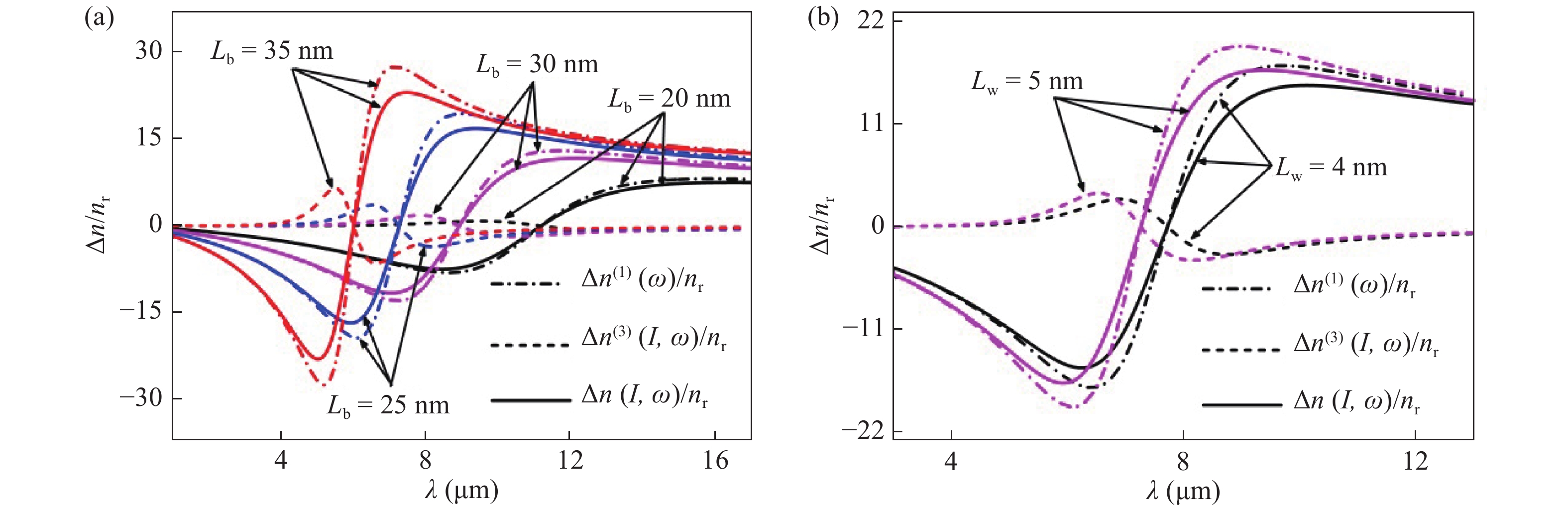
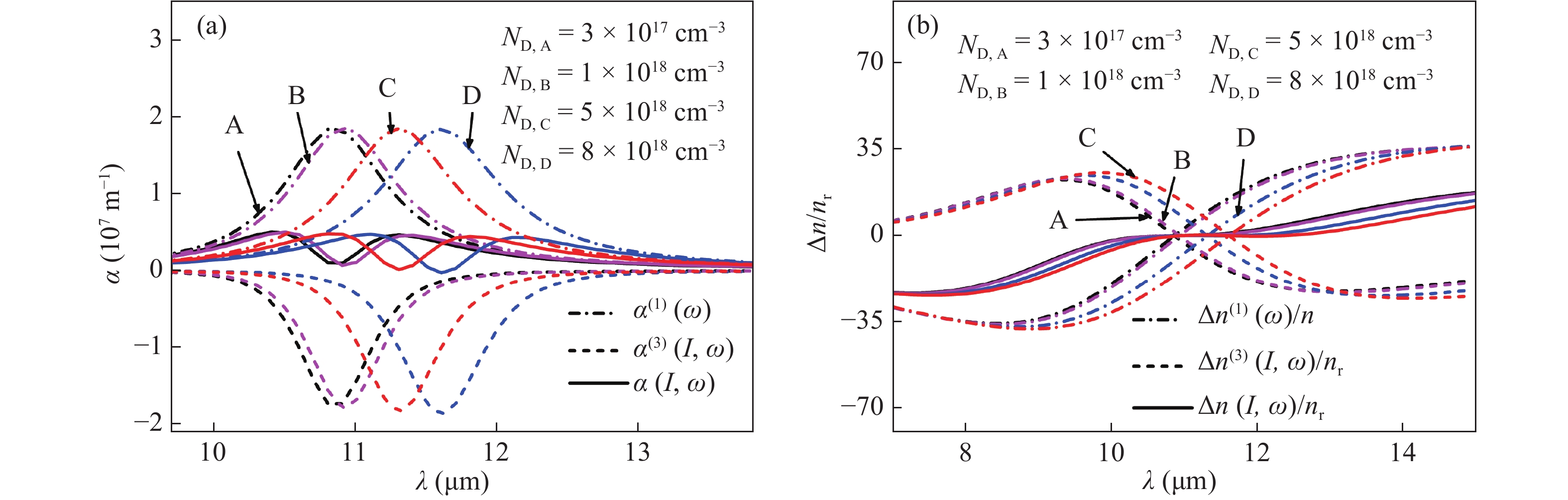
J. Semicond. > 2018, Volume 39 > Issue 12 > 122002

SEMICONDUCTOR PHYSICS

Optical absorption via intersubband transition of electrons in GaAs/AlxGa1−xAs multi-quantum wells in an electric field

Wenqi Zhang, Zhiping Wang and Shiliang Ban

+ Author Affiliations

 Corresponding author: Shiliang Ban, Email: slban@imu.edu.cn

DOI: 10.1088/1674-4926/39/12/122002

PDF

Turn off MathJax

Abstract: Based on the effective mass approximation, the Schrödinger equation and Poisson equation in GaAs/ AlxGa1−xAs multi-quantum wells (MQWs) are self-consistently solved to obtain the wave functions and energy levels of electrons in the conduction band for the ground first excited state by considering a lateral electric field (LEF). Then, the effects of size, ternary mixed crystal, doping concentration, and temperature on linear and nonlinear intersubband optical absorption coefficients (IOACs), and refractive index changes (RICs) due to the transition between ground states and the first excited states of electrons are discussed based on Fermi’s golden rule. The results show that, under a fixed LEF, with increase of Al composition and doping concentration, the IOACs produce a red shift. With increases of both widths of the wells and barriers IOACs appear as blue shifts and their amplitudes increase, but the barrier width change is much more important to affect nonlinear IOACs, whereas increasing the temperature results in a blue shift first and then a red shift of IOACs. When the other parameters are fixed but there is an increase in the LEF, IOACs occur with a blue shift, and the RICs have similar properties.

Key words: optical absorption of electronic intersubband transitionrefractive index changesmulti-quantum wellslateral electric field


[1]
Almodovar C A, Spearrin R M, Hanson R K. Two-color laser absorption near 5 μm for temperature and nitric oxide sensing in high-temperature gases. Journal of Quantitative Spectroscopy & Radiative Transfer, 2017, 203: 572
[2]
Joy S R, Mohammedy F M. Spectral broadening and electron–photon coupling in III–V infrared detectors of low dimensional quantum confined system. Infrared Phys Technol, 2016, 76: 722 doi: 10.1016/j.infrared.2016.04.030
[3]
Sieger M, Haas J, Jetter M, et al. A mid-infrared spectroscopy platform based on GaAs/AlGaAs thin-film waveguides and quantum cascade lasers. Anal Chem, 2016, 88(5): 2558 doi: 10.1021/acs.analchem.5b04144
[4]
Lin T T, Hirayama H. Variable Barrier height AlGaAs/GaAs quantum cascade laser operating at 3.7 THz. Phys Status Solidi, 2017, 114: 1700424
[5]
Mickevičius J, Dobrovolskas D, Aleksiejūnas R, et al. Influence of growth temperature on carrier localization in InGaN/GaN MQWs with strongly redshifted emission band. J Cryst Growth, 2017, 459: 173 doi: 10.1016/j.jcrysgro.2016.12.008
[6]
Mei T, Li H, Karunasiri G, et al. Normal incidence silicon doped p-type GaAs/AlGaAs quantum-well infrared photodetector on (111) A substrate. Infrared Phys Technol, 2007, 50(2/3): 119 doi: 10.1016/j.infrared.2006.10.025
[7]
Dakhlaoui H, Almansour S, Algrafy E. Effect of Si δ-doped layer position on optical absorption in GaAs quantum well under hydrostatic pressure. Superlattices Microstruct, 2015, 77: 196 doi: 10.1016/j.spmi.2014.11.008
[8]
Solaimani M, Morteza I, Arabshahi H, et al. Study of optical non-linear properties of a constant total effective length multiple quantum wells system. J Lumin, 2013, 134(3): 699
[9]
Kong X, Trampert A, Tournie E, et al. Influence of one monolayer thickness variation in GaAs/AlGaAs five-layer asymmetric coupled quantum well upon electrorefractive index change. Jpn J Appl Phys, 2001, 40(2A): 656
[10]
Herrera R A, Ocampo C A A. Effects of geometry and doping level on dispersion and spectrum in GaAs/AlGaAs quantum well waveguide for the near-IR region. J Nonlinear Opt Phys Mater, 2017, 26(03): 1750031 doi: 10.1142/S021886351750031X
[11]
Bilel C, Habchi M M, Nasr A B, et al. Investigation of the doping and Stark effects on the band structure and optical absorption of 1.55 μm GaNAsBi/GaAs MQWs. Curr Appl Phys, 2016, 16(3): 340 doi: 10.1016/j.cap.2015.12.023
[12]
Choi K K, Allen S C, Sun J G, et al. Resonant structures for infrared detection. Appl Opt, 2017, 56(3): B26 doi: 10.1364/AO.56.000B26
[13]
Jani O, Honsberg C. Absorption and transport via tunneling in quantum-well solar cells. Sol Energy Mater Sol Cells, 2006, 90(18/19): 3464 doi: 10.1016/j.solmat.2006.01.004
[14]
Gu Z, Zhu Z N, Wang M M, et al. Interband optical absorption in wurtzite MgxZn1−xO/ZnO/MgyZn1−yO asymmetric quantum wells. Superlattices Microstruct, 2017, 102: 391 doi: 10.1016/j.spmi.2016.10.051
[15]
Nazari M, Karimi M J, Keshavarz A. Linear and nonlinear optical absorption coefficients and refractive index changes in modulation-doped quantum wells: Effects of the magnetic field and hydrostatic pressure. Physica B, 2013, 428(10): 30
[16]
Lei X L, Birman J L, Ting C S. Two-dimensional balance equations in nonlinear electronic transport and application to GaAs‐GaAlAs heterojunctions. J Appl Phys, 1985, 58(6): 2270 doi: 10.1063/1.335945
[17]
Guo A, Du J. Linear and nonlinear optical absorption coefficients and refractive index changes in asymmetrical Gaussian potential quantum wells with applied electric field. Superlattices Microstruct, 2013, 64(12): 158
[18]
Gambhir M, Kumar M, Jha P K, et al. Linear and nonlinear optical absorption coefficients and refractive index changes associated with intersubband transitions in a quantum disk with flat cylindrical geometry. J Lumin, 2013, 143(6): 361
[19]
Vaughn L G, Dawson L R, Pease E A, et al. Type I mid-infrared MQW lasers using AlInAsSb barriers and InAsSb wells. Proc SPIE, 2013: 307
[20]
Chi Y, Shi J. Built-in electric field effect on the linear and nonlinear intersubband optical absorptions in InGaN strained single quantum wells. J Lumin, 2008, 128(11): 1836 doi: 10.1016/j.jlumin.2008.05.006
[21]
Ahn D, Chuang S L. Intersubband optical absorption in a quantum well with an applied electric field. Phys Rev B, 1987, 35(8): 4149 doi: 10.1103/PhysRevB.35.4149
[22]
Ungan F, Yesilgul U, Kasapoglu E, et al. Effects of applied electromagnetic fields on the linear and nonlinear optical properties in an inverse parabolic quantum well. J Lumin, 2012, 132(7): 1627 doi: 10.1016/j.jlumin.2012.02.033
[23]
Sari H, Yesilgul U, Ungan F, et al. Intense laser field effects on the intersubband optical absorption and refractive index change in the δ-doped GaAs quantum wells. Chem Phys, 2017, 487: 11 doi: 10.1016/j.chemphys.2017.02.004
[24]
Vurgaftman I, Meyer J R, Ram-Mohan L R. Band parameters for III–V compound semiconductors and their alloys. J Appl Phys, 2001, 89(11): 5815 doi: 10.1063/1.1368156
[25]
Ha S H, Ban S L, Zhu J. Binding energies of shallow impurities in a symmetric strained wurtzite AlxGa1−xN/GaN/AlyGa1−yN quantum wells. J Semicond, 2011, 32(4): 042001 doi: 10.1088/1674-4926/32/4/042001
[26]
Karimi M J, Rezaei G. Effects of external electric and magnetic fields on the linear and nonlinear intersubband optical properties of finite semi-parabolic quantum dots. Physica B, 2011, 406(23): 4423 doi: 10.1016/j.physb.2011.08.105
[27]
Hutchings D C, Sheikbahae M, Hagan D J, et al. Kramers-Kronig relations in nonlinear optics. Electron Lett, 1990, 26(15): 1206 doi: 10.1049/el:19900780
[28]
Alves F D P, Karunasiri G, Hanson N, et al. NIR, MWIR and LWIR quantum well infrared photodetector using interband and intersubband transitions. Infrared Phys Technol, 2007, 50(2/3): 182 doi: 10.1016/j.infrared.2006.10.021
Fig. 1.  (Color online) A simplified schematic of MQWs with three periodic AlxGa1−xAs/GaAs containing the ground states (dashed lines), first excited states (dotted lines), second excited states (dash-dotted lines), and Fermi energy level (dash-dotted-dotted lines between the ground state and first excited state) in a 30 kV/cm LEF. The widths of the wells, side barriers, and middle barriers are denoted by Lw, Lb, and Lb0, respectively. The energy band offset between the well and barrier is denoted by ΔEg. The arrows in the wells indicate the transition of electrons.

Fig. 2.  (Color online) Electronic wave functions at the ground states (dashed curves), first excited states (dash-dotted curves), and second excited states (dotted curves) in conduction bands (full lines) of (a) a single QW, (b) three QWs, (c) five QWs, and (d) MQWs as a function of z in a 30 kV/cm LEF at ND = 3 × 1017 cm−3, respectively.

Fig. 3.  (Color online) Linear IOACs α(1)(ω) as a function of incident light wavelength λ in a single (short dotted curve) QW, double (dash-dotted-dotted curve), three (dotted curve), four (dash-dotted curve), five (full curve) QWs, and MQWs (dashed curve), respectively.

Fig. 4.  (Color online) Under a 30 kV/cm LEF with ND = 3 × 1017 cm−3, (a) α(1)(ω) (dash-dotted curves), α(3)(I, ω) (dashed curves), and α(I, ω) (full curves), (b) Δn(1)(ω)/nr (dash-dotted curves), Δn(3)(I, ω)/nr (dashed curves), and Δn(I, ω)/nr (full curves) as functions of incident light wavelength λ with Al components x = 0.1, 0.23, and 0.39, respectively.

Fig. 5.  (Color online) Under a 30 kV/cm LEF with ND = 3 × 1017 cm−3, α(1)(ω) (dash-dotted curves), α(3)(I, ω) (dashed curves), and α(I, ω) (full curves) as functions of incident light wavelength λ with (a) Lb = 20, 25, 30, 35 nm, and (b) Lw = 4, 4.5, 5, 5.5 nm, respectively.

Fig. 6.  (Color online) Under a 30 kV/cm LEF with ND = 3 × 1017 cm−3, Δn(1)(ω)/nr (dash-dotted curves), Δn(3)(I, ω)/nr (dashed curves), and Δn(I, ω)/nr (full curves) as functions of incident light wavelength λ with (a) Lb = 20, 30, 35 nm, and (b) Lw = 4, 5 nm, respectively.

Fig. 7.  (Color online) Under a 30 kV/cm LEF with Lw = 5 nm, (a) α(1)(ω) (dash-dotted curves), α(3)(I, ω) (dashed curves), and α(I, ω) (full curves), (b) Δn(1)(ω)/nr (dash-dotted curves), Δn(3)(I, ω)/nr (dashed curves), and Δn(I, ω)/nr (full curves) as functions of incident light wavelength λ with ND = 3 × 10¹⁷, 1 × 10¹⁸, 5 × 10¹⁸, and 8 × 1018 cm−3, respectively.

Fig. 8.  (Color online) α(1)(ω) as a function of incident light wavelength λ with Lw = 5 nm in a 30 kV/cm LEF at temperature T = 77 (full curves), 200 (dashed curves), and 300 K (dotted curves), respectively.

Fig. 9.  (Color online) α(I, ω) as a function of incident light wavelength λ for LEF = 0 (full curve), 35 (dotted curve), 65 (dash-dotted-dotted curve), 80 (dash-dotted curve), and 100 (short dotted curve) kV/cm, respectively.

Fig. 10.  Comparison of IOACs calculated (solid curves) in (a) AlGaAs/GaAs MQWs, and (b) AlGaAs/GaAs/InGaAs MQWs as a function of wavelength λ with that of experimental values (dotted curves).

Table 1.   Parameters used in numerical calculations.

Parameter AlAs GaAs AlxGa1−xAs
Eg (eV) 3.09a 1.519a 3.09x + 1.519(1 − x)b
mi*(m0) 0.15a 0.067a 0.15x + 0.067(1 − x)b
εr (ε0) 10.8a 13.18a 10.8x + 13.18(1 − x)b
a Ref. [24]. b Ref. [25].
DownLoad: CSV
[1]
Almodovar C A, Spearrin R M, Hanson R K. Two-color laser absorption near 5 μm for temperature and nitric oxide sensing in high-temperature gases. Journal of Quantitative Spectroscopy & Radiative Transfer, 2017, 203: 572
[2]
Joy S R, Mohammedy F M. Spectral broadening and electron–photon coupling in III–V infrared detectors of low dimensional quantum confined system. Infrared Phys Technol, 2016, 76: 722 doi: 10.1016/j.infrared.2016.04.030
[3]
Sieger M, Haas J, Jetter M, et al. A mid-infrared spectroscopy platform based on GaAs/AlGaAs thin-film waveguides and quantum cascade lasers. Anal Chem, 2016, 88(5): 2558 doi: 10.1021/acs.analchem.5b04144
[4]
Lin T T, Hirayama H. Variable Barrier height AlGaAs/GaAs quantum cascade laser operating at 3.7 THz. Phys Status Solidi, 2017, 114: 1700424
[5]
Mickevičius J, Dobrovolskas D, Aleksiejūnas R, et al. Influence of growth temperature on carrier localization in InGaN/GaN MQWs with strongly redshifted emission band. J Cryst Growth, 2017, 459: 173 doi: 10.1016/j.jcrysgro.2016.12.008
[6]
Mei T, Li H, Karunasiri G, et al. Normal incidence silicon doped p-type GaAs/AlGaAs quantum-well infrared photodetector on (111) A substrate. Infrared Phys Technol, 2007, 50(2/3): 119 doi: 10.1016/j.infrared.2006.10.025
[7]
Dakhlaoui H, Almansour S, Algrafy E. Effect of Si δ-doped layer position on optical absorption in GaAs quantum well under hydrostatic pressure. Superlattices Microstruct, 2015, 77: 196 doi: 10.1016/j.spmi.2014.11.008
[8]
Solaimani M, Morteza I, Arabshahi H, et al. Study of optical non-linear properties of a constant total effective length multiple quantum wells system. J Lumin, 2013, 134(3): 699
[9]
Kong X, Trampert A, Tournie E, et al. Influence of one monolayer thickness variation in GaAs/AlGaAs five-layer asymmetric coupled quantum well upon electrorefractive index change. Jpn J Appl Phys, 2001, 40(2A): 656
[10]
Herrera R A, Ocampo C A A. Effects of geometry and doping level on dispersion and spectrum in GaAs/AlGaAs quantum well waveguide for the near-IR region. J Nonlinear Opt Phys Mater, 2017, 26(03): 1750031 doi: 10.1142/S021886351750031X
[11]
Bilel C, Habchi M M, Nasr A B, et al. Investigation of the doping and Stark effects on the band structure and optical absorption of 1.55 μm GaNAsBi/GaAs MQWs. Curr Appl Phys, 2016, 16(3): 340 doi: 10.1016/j.cap.2015.12.023
[12]
Choi K K, Allen S C, Sun J G, et al. Resonant structures for infrared detection. Appl Opt, 2017, 56(3): B26 doi: 10.1364/AO.56.000B26
[13]
Jani O, Honsberg C. Absorption and transport via tunneling in quantum-well solar cells. Sol Energy Mater Sol Cells, 2006, 90(18/19): 3464 doi: 10.1016/j.solmat.2006.01.004
[14]
Gu Z, Zhu Z N, Wang M M, et al. Interband optical absorption in wurtzite MgxZn1−xO/ZnO/MgyZn1−yO asymmetric quantum wells. Superlattices Microstruct, 2017, 102: 391 doi: 10.1016/j.spmi.2016.10.051
[15]
Nazari M, Karimi M J, Keshavarz A. Linear and nonlinear optical absorption coefficients and refractive index changes in modulation-doped quantum wells: Effects of the magnetic field and hydrostatic pressure. Physica B, 2013, 428(10): 30
[16]
Lei X L, Birman J L, Ting C S. Two-dimensional balance equations in nonlinear electronic transport and application to GaAs‐GaAlAs heterojunctions. J Appl Phys, 1985, 58(6): 2270 doi: 10.1063/1.335945
[17]
Guo A, Du J. Linear and nonlinear optical absorption coefficients and refractive index changes in asymmetrical Gaussian potential quantum wells with applied electric field. Superlattices Microstruct, 2013, 64(12): 158
[18]
Gambhir M, Kumar M, Jha P K, et al. Linear and nonlinear optical absorption coefficients and refractive index changes associated with intersubband transitions in a quantum disk with flat cylindrical geometry. J Lumin, 2013, 143(6): 361
[19]
Vaughn L G, Dawson L R, Pease E A, et al. Type I mid-infrared MQW lasers using AlInAsSb barriers and InAsSb wells. Proc SPIE, 2013: 307
[20]
Chi Y, Shi J. Built-in electric field effect on the linear and nonlinear intersubband optical absorptions in InGaN strained single quantum wells. J Lumin, 2008, 128(11): 1836 doi: 10.1016/j.jlumin.2008.05.006
[21]
Ahn D, Chuang S L. Intersubband optical absorption in a quantum well with an applied electric field. Phys Rev B, 1987, 35(8): 4149 doi: 10.1103/PhysRevB.35.4149
[22]
Ungan F, Yesilgul U, Kasapoglu E, et al. Effects of applied electromagnetic fields on the linear and nonlinear optical properties in an inverse parabolic quantum well. J Lumin, 2012, 132(7): 1627 doi: 10.1016/j.jlumin.2012.02.033
[23]
Sari H, Yesilgul U, Ungan F, et al. Intense laser field effects on the intersubband optical absorption and refractive index change in the δ-doped GaAs quantum wells. Chem Phys, 2017, 487: 11 doi: 10.1016/j.chemphys.2017.02.004
[24]
Vurgaftman I, Meyer J R, Ram-Mohan L R. Band parameters for III–V compound semiconductors and their alloys. J Appl Phys, 2001, 89(11): 5815 doi: 10.1063/1.1368156
[25]
Ha S H, Ban S L, Zhu J. Binding energies of shallow impurities in a symmetric strained wurtzite AlxGa1−xN/GaN/AlyGa1−yN quantum wells. J Semicond, 2011, 32(4): 042001 doi: 10.1088/1674-4926/32/4/042001
[26]
Karimi M J, Rezaei G. Effects of external electric and magnetic fields on the linear and nonlinear intersubband optical properties of finite semi-parabolic quantum dots. Physica B, 2011, 406(23): 4423 doi: 10.1016/j.physb.2011.08.105
[27]
Hutchings D C, Sheikbahae M, Hagan D J, et al. Kramers-Kronig relations in nonlinear optics. Electron Lett, 1990, 26(15): 1206 doi: 10.1049/el:19900780
[28]
Alves F D P, Karunasiri G, Hanson N, et al. NIR, MWIR and LWIR quantum well infrared photodetector using interband and intersubband transitions. Infrared Phys Technol, 2007, 50(2/3): 182 doi: 10.1016/j.infrared.2006.10.021
1

ZnO1-xTex and ZnO1-xSx semiconductor alloys as competent materials for opto-electronic and solar cell applications:a comparative analysis

Utsa Das, Partha P. Pal

Journal of Semiconductors, 2017, 38(8): 082001. doi: 10.1088/1674-4926/38/8/082001

2

Performance analysis of charge plasma based dual electrode tunnel FET

Sunny Anand, S. Intekhab Amin, R. K. Sarin

Journal of Semiconductors, 2016, 37(5): 054003. doi: 10.1088/1674-4926/37/5/054003

3

Donor impurity-related optical absorption coefficients and refractive index changes in a rectangular GaAs quantum dot in the presence of electric field

Sheng Wang, Yun Kang, Xianli Li

Journal of Semiconductors, 2016, 37(11): 112001. doi: 10.1088/1674-4926/37/11/112001

4

Effect of electric field on metallic SWCNT interconnects for nanoscale technologies

Harsimran Kaur, Karamjit Singh Sandha

Journal of Semiconductors, 2015, 36(3): 035001. doi: 10.1088/1674-4926/36/3/035001

5

Analysis of charge density and Fermi level of AlInSb/InSb single-gate high electron mobility transistor

S. Theodore Chandra, N. B. Balamurugan, M. Bhuvaneswari, N. Anbuselvan, N. Mohankumar, et al.

Journal of Semiconductors, 2015, 36(6): 064003. doi: 10.1088/1674-4926/36/6/064003

6

Electrical properties of Ge:Ga near the metal-insulator transition

M Errai, A El Kaaouachi, H El Idrissi

Journal of Semiconductors, 2015, 36(6): 062001. doi: 10.1088/1674-4926/36/6/062001

7

Influences of ICP etching damages on the electronic properties of metal field plate 4H-SiC Schottky diodes

Hui Wang, Yingxi Niu, Fei Yang, Yong Cai, Zehong Zhang, et al.

Journal of Semiconductors, 2015, 36(10): 104006. doi: 10.1088/1674-4926/36/10/104006

8

The influence of the channel electric field distribution on the polarization Coulomb field scattering in AlN/GaN heterostructure field-effect transistors

Yingxia Yu, Zhaojun Lin, Yuanjie Lü, Zhihong Feng, Chongbiao Luan, et al.

Journal of Semiconductors, 2014, 35(12): 124007. doi: 10.1088/1674-4926/35/12/124007

9

In situ TEM/SEM electronic/mechanical characterization of nano material with MEMS chip

Yuelin Wang, Tie Li, Xiao Zhang, Hongjiang Zeng, Qinhua Jin, et al.

Journal of Semiconductors, 2014, 35(8): 081001. doi: 10.1088/1674-4926/35/8/081001

10

The effects of electron irradiation on the optical properties of the organic semiconductor polypyrrole

J. V. Thombare, M. C. Rath, S. H. Han, V. J. Fulari

Journal of Semiconductors, 2013, 34(9): 093001. doi: 10.1088/1674-4926/34/9/093001

11

Correlation between electrical conductivity-optical band gap energy and precursor molarities ultrasonic spray deposition of ZnO thin films

Said Benramache, Okba Belahssen, Abderrazak Guettaf, Ali Arif

Journal of Semiconductors, 2013, 34(11): 113001. doi: 10.1088/1674-4926/34/11/113001

12

Structural parameters improvement of an integrated HBT in a cascode configuration opto-electronic mixer

Hassan Kaatuzian, Hadi Dehghan Nayeri, Masoud Ataei, Ashkan Zandi

Journal of Semiconductors, 2013, 34(9): 094001. doi: 10.1088/1674-4926/34/9/094001

13

Structural, electronic, magnetic and optical properties of neodymium chalcogenides using LSDA+U method

A Shankar, D P Rai, Sandeep, R K Thapa

Journal of Semiconductors, 2012, 33(8): 082001. doi: 10.1088/1674-4926/33/8/082001

14

Optical and electrical properties of electrochemically deposited polyaniline-CeO2 hybrid nanocomposite film

Anees A. Ansari, M. A. M. Khan, M. Naziruddin Khan, Salman A. Alrokayan, M. Alhoshan, et al.

Journal of Semiconductors, 2011, 32(4): 043001. doi: 10.1088/1674-4926/32/4/043001

15

The Bipolar Field-Effect Transistor: VIII. Longitudinal Gradient of Longitudinal Electric Field (Two-MOS-Gates on Pure-Base)

Jie Binbin, Sah Chihtang

Journal of Semiconductors, 2010, 31(7): 071001. doi: 10.1088/1674-4926/31/7/071001

16

Frequency of the transition spectral line of an electron in quantum rods

Wang Guiwen, Xiao Jinglin

Journal of Semiconductors, 2010, 31(9): 092002. doi: 10.1088/1674-4926/31/9/092002

17

Influence of optical phonons on the electronic mobility in a strained wurtzite AlN/GaN heterojunction under hydrostatic pressure

Zhou Xiaojuan, Ban Shiliang

Journal of Semiconductors, 2009, 30(8): 082001. doi: 10.1088/1674-4926/30/8/082001

18

Influence of Polarization-Induced Electric Fields on Optical Properties of Intersubband Transitions in AlxGa1-xN/GaN Double Quantum Wells

Lei Shuangying, Shen Bo, Xu Fujun, Yang Zhijian, Xu Ke, et al.

Chinese Journal of Semiconductors , 2006, 27(3): 403-408.

19

Full Band Monte Carlo Simulation of Electron Transport in Ge with Anisotropic Scattering Process

Chen, Yong, and, Ravaioli, Umberto, et al.

Chinese Journal of Semiconductors , 2005, 26(3): 465-471.

20

A Wavelength Tunable DBR Laser Integrated with an Electro-Absorption Modulator by a Combined Method of SAG and QWI

Zhang Jing, Li Baoxia, Zhao Lingjuan, Wang Baojun, Zhou Fan, et al.

Chinese Journal of Semiconductors , 2005, 26(11): 2053-2057.

1. Jaouane, M., Ed-Dahmouny, A., Arraoui, R. et al. Delta-doping modulation of three quantum wells under the influence of an electric field. APL Materials, 2024, 12(10): 101106. doi:10.1063/5.0231797
2. Qasem, M.R., Falyouni, F., Elamri, F.-Z. et al. Electronic states in GaAs/Ga1−xAlxAs/GaAs MQWs induced by two defect layers. Physica B: Condensed Matter, 2023. doi:10.1016/j.physb.2021.413228
3. Martínez-Orozco, J.C., Ungan, F., Rodríguez-Magdaleno, K.A. Studies on the nonlinear optical properties of two-step GaAs/Ga1-xAlxAs quantum well. Physica Scripta, 2020, 95(3): 035802. doi:10.1088/1402-4896/ab4acd
  • Search

    Advanced Search >>

    GET CITATION

    Shi Zhaoxia, Zhu Dazhong. Modeling and discussion of threshold voltage for a multi-floating gate FET pH sensor[J]. Journal of Semiconductors, 2009, 30(11): 114011. doi: 10.1088/1674-4926/30/11/114011
    Shi Z X, Zhu D Z. Modeling and discussion of threshold voltage for a multi-floating gate FET pH sensor[J]. J. Semicond., 2009, 30(11): 114011. doi: 10.1088/1674-4926/30/11/114011.
    shu

    Export: BibTex EndNote

    Article Metrics

    Article views: 4095 Times PDF downloads: 83 Times Cited by: 3 Times

    History

    Received: 23 March 2018 Revised: 19 April 2018 Online: Uncorrected proof: 29 June 2018Accepted Manuscript: 01 November 2018Corrected proof: 01 November 2018Published: 13 December 2018

    Catalog

      Email This Article

      User name:
      Email:*请输入正确邮箱
      Code:*验证码错误
      Wenqi Zhang, Zhiping Wang, Shiliang Ban. Optical absorption via intersubband transition of electrons in GaAs/AlxGa1−xAs multi-quantum wells in an electric field[J]. Journal of Semiconductors, 2018, 39(12): 122002. doi: 10.1088/1674-4926/39/12/122002 ****W Q Zhang, Z P Wang, S L Ban, Optical absorption via intersubband transition of electrons in GaAs/AlxGa1−xAs multi-quantum wells in an electric field[J]. J. Semicond., 2018, 39(12): 122002. doi: 10.1088/1674-4926/39/12/122002.
      Citation:
      Wenqi Zhang, Zhiping Wang, Shiliang Ban. Optical absorption via intersubband transition of electrons in GaAs/AlxGa1−xAs multi-quantum wells in an electric field[J]. Journal of Semiconductors, 2018, 39(12): 122002. doi: 10.1088/1674-4926/39/12/122002 ****
      W Q Zhang, Z P Wang, S L Ban, Optical absorption via intersubband transition of electrons in GaAs/AlxGa1−xAs multi-quantum wells in an electric field[J]. J. Semicond., 2018, 39(12): 122002. doi: 10.1088/1674-4926/39/12/122002.

      Optical absorption via intersubband transition of electrons in GaAs/AlxGa1−xAs multi-quantum wells in an electric field

      DOI: 10.1088/1674-4926/39/12/122002
      Funds:

      Project supported by the National Natural Science Foundation of China (No. 61764012).

      More Information
      • Corresponding author: Email: slban@imu.edu.cn
      • Received Date: 2018-03-23
      • Revised Date: 2018-04-19
      • Published Date: 2018-12-01

      Catalog

        /

        DownLoad:  Full-Size Img  PowerPoint
        Return
        Return