


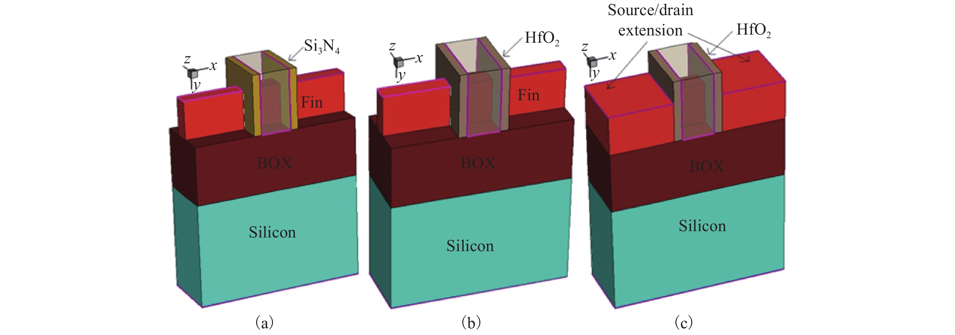
Fig. 1.
(Color online) (a) Device-D1 (conventional Si3N4 spacer SOI FinFET). (b) Device-D2 (conventional HfO2 SOI FinFET). (c) Device-D3 (source/drain extended HfO2 spacer SOI FinFET).
SEMICONDUCTOR DEVICES
Corresponding author: Neeraj Jain, E-mail: erneerajjain@gmail.com; Balwinder Raj, balwinderraj@gmail.com
Abstract: Nowadays FinFET devices have replaced the MOS devices almost in all complex integrated circuits of electronic gadgets like computer peripherals, tablets, and smartphones in portable electronics. The scaling of FinFET is ongoing and the analog/RF performance is most affected by increased SCEs (short channel effects) in sub 22 nm technology nodes. This paper explores the analog/RF performance study and analysis of high performance device-D2 (conventional HfO2 spacer SOI FinFET) and device-D3 (source/drain extended HfO2 spacer SOI FinFET) over the device-D1 (conventional Si3N4 spacer SOI FinFET) at 20 nm technology node through the 3-D (dimensional) simulation process. The major performance parameters like Ion (ON current), Ioff (OFF current), gm (transconductance), gd (output conductance), AV (intrinsic gain), SS (sub-threshold slope), TGF = gm/Id (trans-conductance generation factor), VEA (early voltage), GTFP (gain trans-conductance frequency product), TFP (tans-conductance frequency product), GFP (gain frequency product), and fT (cut-off frequency) are studied for evaluating the analog/RF performance of different flavored SOI FinFET structures. For analog performance evaluation, device-D3 and D2 give better results in terms of gm, ID (drain current) and SS parameters, and for RF performance evaluation device-D1 is better in terms of fT, GTFP, TFP, and GFP parameters both at low and high values of VDS = 0.05 V and VDS = 0.7 V respectively.
Keywords: SOI FinFET, SCEs, intrinsic gain, trans-conductance, cut-off frequency
| [1] |
Moore G E. Cramming more components onto integrated circuits. Proc IEEE, 1998, 86(1): 82 doi: 10.1109/JPROC.1998.658762
|
| [2] |
Veeraraghavan S, Fossum J G. Short-channel effects in SOI MOSFET’s. IEEE Trans Electron Devices, 1989, 36(3): 522 doi: 10.1109/16.19963
|
| [3] |
Liu Y, Ishii K, Masahara M, et al. Cross-sectional channel shape dependence of short-channel effects in fin-type double-gate metal oxide semiconductor field-effect transistors. Jpn J Appl Phys, 2004, 43(4S): 2151
|
| [4] |
Colinge J P. Multiple-gate SOI MOSFETs. Solid State Electron, 2004, 48(6): 897 doi: 10.1016/j.sse.2003.12.020
|
| [5] |
Colinge J P, Chandrakasan A. FinFETs and other multi-gate transistors. Springer, 2008
|
| [6] |
Bhattacharya D, Jha N K. FinFETs: from devices to architectures. Adv Electron, 2014
|
| [7] |
ITRS. International technology roadmap for semiconductors, 2013; Executive Summary Itrs 80
|
| [8] |
Fahad H M, Hu C, Hussain M M. Simulation study of a 3-D device integrating FinFET and UTBFET. IEEE Trans Electron Devices, 2015, 62(1): 83 doi: 10.1109/TED.2014.2372695
|
| [9] |
Hisamoto D, Lee W C, Kedzierski J, et al. FinFET-A self-aligned double-gate MOSFET scalable to 20 nm. IEEE Trans Electron Devices, 2000, 47(12): 2320 doi: 10.1109/16.887014
|
| [10] |
Nowak E J, Aller I, Ludwig T, et al. Turning silicon on its edge double gate CMOS/FinFET technology. Circuits Devices Mag IEEE, 2004, 20(1): 20 doi: 10.1109/MCD.2004.1263404
|
| [11] |
Pal P K, Kaushik B K , Dasgupta S. Investigation of symmetric dual-k spacer trigate FinFETs from delay perspective. IEEE Trans Electron Devices, 2014, 61(11): 3579 doi: 10.1109/TED.2014.2351616
|
| [12] |
Pal P K, Kaushik B K, Dasgupta S. High-performance and robust SRAM cell based on asymmetric dual-k spacer FinFETs. IEEE Trans Electron Devices, 2013, 60(10): 3371 doi: 10.1109/TED.2013.2278201
|
| [13] |
Park J T, Colinge J P, Diaz C H. Pi-gate SOI MOSFET. IEEE Electron Device Lett, 2001, 22(8): 405 doi: 10.1109/55.936358
|
| [14] |
Singh N, Lim F Y, Fang W W, et al. Ultra-narrow silicon nanowire gate-all-around CMOS devices: Impact of diameter, channel-orientation and low temperature on device performance. Technical Digest - International Electron Devices Meeting, 2006
|
| [15] |
Raj B, Saxena A K, Dasgupta S. Analytical modeling for the estimation of leakage current and subthreshold swing factor of nanoscale double gate FinFET device. Microelectron Int, 2009, 26(1): 53 doi: 10.1108/13565360910923188
|
| [16] |
Sharma V K, Pattanaik M, Raj B. INDEP approach for leakage reduction in nanoscale CMOS circuits. Int J Electron, 2015, 102(2): 200 doi: 10.1080/00207217.2014.896042
|
| [17] |
Raj B. Quantum mechanical potential modeling of FinFET toward quantum FinFET. Springer, 2013
|
| [18] |
Raj B, Saxena A K, Dasgupta S. A compact drain current and threshold voltage quantum mechanical analytical modeling for FinFETs. J Nanoelectron Optoelectron, 2008, 3(2): 163 doi: 10.1166/jno.2008.209
|
| [19] |
ITRS. ERD Working Group. International Technology Roadmap for Semiconductors, Edition - Emerging Research Devices Challenges, 2011
|
| [20] |
Magnone P, Mercha A, Subramanian V, et al. Matching performance of FinFET devices with fin widths down to 10 nm. IEEE Electron Device Lett, 2009, 30(12): 1374 doi: 10.1109/LED.2009.2034117
|
| [21] |
http://www.synopsys.com. Sentaurus TCAD User’s Manual
|
| [22] |
Mohapatra S K, Pradhan K P, Singh D, et al. The role of geometry parameters and fin aspect ratio of sub-20 nm SOI-FinFET: an analysis towards analog and RF circuit design. IEEE Trans Nanotechnol, 2015, 14(3): 546 doi: 10.1109/TNANO.2015.2415555
|
| [23] |
Pradhan K P, Mohapatra S K, Sahu P K, et al. Impact of high-k gate dielectric on analog and RF performance of nanoscale DG-MOSFET. Microelectron J, 2014, 45(2): 144 doi: 10.1016/j.mejo.2013.11.016
|
| [24] |
Ho B, Sun X, Shin C, et al. Design optimization of multigate bulk MOSFETs. IEEE Trans Electron Devices, 2013, 60(1): 28 doi: 10.1109/TED.2012.2224870
|
| [25] |
De Andrade M G C, Martino J A, Aoulaiche M, et al. Behavior of triple-gate bulk FinFETs with and without DTMOS operation. Solid-State Electron, 2012, 71: 63 doi: 10.1016/j.sse.2011.10.022
|
| [26] |
Pradhan K P, Sahu P K , Mohapatra S K. Analysis of symmetric high-k spacer (SHS) trigate wavy FinFET: a novel device. India Conference (INDICON), 2 Annual IEEE (IEEE),2015: 1
|
| [27] |
Canali C, Majni G, Minder R, et al. Electron and hole drift velocity measurements in silicon and their empirical relation to electric field and temperature. IEEE Trans Electron Devices, 1975, 22(11): 1045 doi: 10.1109/T-ED.1975.18267
|
| [28] |
Lombardi C, Manzini S, Saporito A, et al. A physically based mobility model for numerical simulation of nonplanar devices. IEEE Trans Comput Des Integr Circuits Syst, 1988, 7(11): 1164 doi: 10.1109/43.9186
|
| [29] |
Shockley W, Read W T. Statistics of the recombination of holes and electrons. Phys Rev, 1952, 87(46): 835
|
| [30] |
Hall R N. Electron–hole recombination in germanium. Phys Rev, 1952, 87(2): 387
|
| [31] |
Sze S M, Ng K K. Physics of semiconductor devices. NJ: John Wiley Sons, 2007
|
| [32] |
Sarkar A, Das A K, De S, et al. Effect of gate engineering in double-gate MOSFETs for analog/RF applications. Microelectron J, 2012, 43(11): 873 doi: 10.1016/j.mejo.2012.06.002
|
Table 1. Dimensional values used for simulation in this paper (unit: nm).
| Parameter | Description | Device-D1 | Device-D2 | Device-D3 |
| WFin | Fin width | 10 | 10 | 10 |
| HFin | Fin height | 26 | 26 | 26 |
| Lg | Gate channel length | 20 | 20 | 20 |
| tox | Oxide thickness | 0.9 | 0.9 | 0.9 |
| BOX | Thickness of the buried oxide | 40 | 40 | 40 |
| W | Effective width of transistor | 62 | 62 | 62 |
| L | The total length of the device | 110 | 110 | 110 |
| Llk | Spacer length (Si3N4, k = 7.5) | 5 | – | – |
| Lhk | Spacer length (HfO2, k = 22) | – | 5 | 5 |
| Ws/d | Source/drain width | 10 | 10 | 40 |
 DownLoad: CSV
Table 2. Electrostatic SCEs parameters.
| Device | SS (mV/decade) | Ion (μA) | Ioff (nA) | DIBL (mV/V) | |||||
| VDS = 0.7 V | VDS = 0.05 V | VDS = 0.7 V | VDS = 0.05 V | VDS = 0.7 V | VDS = 0.05 V | ||||
| D1 | 71.56 | 67.69 | 61.0 | 33.0 | 12.5 | 5.65 | 30.37 | ||
| D2 | 68.93 | 66.17 | 89.0 | 46.6 | 25.3 | 13.9 | 70.76 | ||
| D3 | 68.89 | 66.41 | 100 | 57.7 | 58.6 | 30.5 | 81.53 | ||
DownLoad: CSV
Table 3. Analog performance of device D1, D2, and D3 for VDS = 0.7 V and VDS = 0.05 V.
| Device | gm (S) | gd (S) | AV (dB) | TGF (V−1) | VEA (V) | ||||||
| VDS = 0.05 V | VDS = 0.7 V | VDS = 0.7 V | VDS = 0.7 V | VDS = 0.05 V | VDS = 0.7 V | VDS = 0.7 V | |||||
| D1 | 9.04 × 10⁻⁵ | 1.9 × 10⁻⁴ | 4.39 × 10⁻⁶ | 30.01 | 36.90 | 35.08 | 5.30 | ||||
| D2 | 1.06 × 10⁻⁴ | 1.80 × 10⁻⁴ | 4.0 × 10⁻⁶ | 33.06 | 37.92 | 35.97 | 6.35 | ||||
| D3 | 1.24 × 10⁻⁴ | 2.01 × 10⁻⁴ | 4.71 × 10⁻⁶ | 32.60 | 37.21 | 34.60 | 6.45 | ||||
DownLoad: CSV
Table 4. RF Performance of Device D1, D2, and D3 at VDS = 0.05 V.
| Device | Cgd (aF) | Cgs (aF) | GTFP (GHz) | TFP (GHz/V) | GFP (GHz) | fT (GHz) |
| D1 | 33.4 | 35.6 | 6.44 × 10⁴ | 1.11 × 10³ | 1.13 × 10⁴ | 195.83 |
| D2 | 54.9 | 57.6 | 8.70 × 10⁴ | 1.40 × 10³ | 1.83 × 10⁴ | 132.45 |
| D3 | 78.8 | 84.6 | 3.63 × 10⁴ | 5.66 × 10² | 7.49 × 10³ | 116.86 |
DownLoad: CSV
Table 5. RF Performance of Device D1, D2, and D3 at VDS = 0.7 V.
| Device | Cgd (aF) | Cgs (aF) | GTFP (GHz) | TFP (GHz/V) | GFP (GHz) | fT (GHz) |
| D1 | 8.35 | 44.4 | 1.22 × 10⁵ | 2.79 × 10³ | 1.82 × 10⁴ | 413.15 |
| D2 | 14.6 | 73.1 | 7.48 × 10⁴ | 1.82 × 10³ | 1.22 × 10⁴ | 296.29 |
| D3 | 41.6 | 99.4 | 3.18 × 10⁴ | 1.14 × 10³ | 5.67 × 10³ | 202.09 |
DownLoad: CSV
Table 6. Simulated results at different spacer length for SOI FinFET at VDS = 0.7 V.
| Device spacer region, Lsp, hk | SS (mV/decade) | Ion (μA) | Ioff (nA) | Ion/Ioff | TGF (V−1) | gm (S) | gd (S) | Cgg (fF) | fT (GHz) | Gain, AV(gm/gd) (dB) |
| 2 nm | 83.53 | 106.80 | 185.85 | 574.7 | 25 | 2.15 × 10⁻⁴ | 1.14 × 10⁻⁵ | 0.210 | 163 | 25.5 |
| 5 nm | 69.89 | 100.23 | 58.56 | 1711.6 | 32.5 | 2.02 × 10⁻⁴ | 5.54 × 10⁻⁶ | 0.150 | 215 | 31.24 |
| 8 nm | 66.62 | 96.80 | 39.83 | 2430.3 | 34.9 | 1.96 × 10⁻⁴ | 4.14 × 10⁻⁶ | 0.133 | 235 | 33.50 |
| 12 nm | 65.11 | 92.56 | 31.36 | 2951.5 | 36.1 | 1.89 × 10⁻⁴ | 2.25 × 10⁻⁶ | 0.137 | 219 | 38.48 |
| 16 nm | 65.12 | 31.23 | 2.19 | 14 260.3 | 39.3 | 4.35 × 10⁻⁵ | 7.30 × 10⁻⁷ | 0.681 | 102 | 35.50 |
DownLoad: CSV
| [1] |
Moore G E. Cramming more components onto integrated circuits. Proc IEEE, 1998, 86(1): 82 doi: 10.1109/JPROC.1998.658762
|
| [2] |
Veeraraghavan S, Fossum J G. Short-channel effects in SOI MOSFET’s. IEEE Trans Electron Devices, 1989, 36(3): 522 doi: 10.1109/16.19963
|
| [3] |
Liu Y, Ishii K, Masahara M, et al. Cross-sectional channel shape dependence of short-channel effects in fin-type double-gate metal oxide semiconductor field-effect transistors. Jpn J Appl Phys, 2004, 43(4S): 2151
|
| [4] |
Colinge J P. Multiple-gate SOI MOSFETs. Solid State Electron, 2004, 48(6): 897 doi: 10.1016/j.sse.2003.12.020
|
| [5] |
Colinge J P, Chandrakasan A. FinFETs and other multi-gate transistors. Springer, 2008
|
| [6] |
Bhattacharya D, Jha N K. FinFETs: from devices to architectures. Adv Electron, 2014
|
| [7] |
ITRS. International technology roadmap for semiconductors, 2013; Executive Summary Itrs 80
|
| [8] |
Fahad H M, Hu C, Hussain M M. Simulation study of a 3-D device integrating FinFET and UTBFET. IEEE Trans Electron Devices, 2015, 62(1): 83 doi: 10.1109/TED.2014.2372695
|
| [9] |
Hisamoto D, Lee W C, Kedzierski J, et al. FinFET-A self-aligned double-gate MOSFET scalable to 20 nm. IEEE Trans Electron Devices, 2000, 47(12): 2320 doi: 10.1109/16.887014
|
| [10] |
Nowak E J, Aller I, Ludwig T, et al. Turning silicon on its edge double gate CMOS/FinFET technology. Circuits Devices Mag IEEE, 2004, 20(1): 20 doi: 10.1109/MCD.2004.1263404
|
| [11] |
Pal P K, Kaushik B K , Dasgupta S. Investigation of symmetric dual-k spacer trigate FinFETs from delay perspective. IEEE Trans Electron Devices, 2014, 61(11): 3579 doi: 10.1109/TED.2014.2351616
|
| [12] |
Pal P K, Kaushik B K, Dasgupta S. High-performance and robust SRAM cell based on asymmetric dual-k spacer FinFETs. IEEE Trans Electron Devices, 2013, 60(10): 3371 doi: 10.1109/TED.2013.2278201
|
| [13] |
Park J T, Colinge J P, Diaz C H. Pi-gate SOI MOSFET. IEEE Electron Device Lett, 2001, 22(8): 405 doi: 10.1109/55.936358
|
| [14] |
Singh N, Lim F Y, Fang W W, et al. Ultra-narrow silicon nanowire gate-all-around CMOS devices: Impact of diameter, channel-orientation and low temperature on device performance. Technical Digest - International Electron Devices Meeting, 2006
|
| [15] |
Raj B, Saxena A K, Dasgupta S. Analytical modeling for the estimation of leakage current and subthreshold swing factor of nanoscale double gate FinFET device. Microelectron Int, 2009, 26(1): 53 doi: 10.1108/13565360910923188
|
| [16] |
Sharma V K, Pattanaik M, Raj B. INDEP approach for leakage reduction in nanoscale CMOS circuits. Int J Electron, 2015, 102(2): 200 doi: 10.1080/00207217.2014.896042
|
| [17] |
Raj B. Quantum mechanical potential modeling of FinFET toward quantum FinFET. Springer, 2013
|
| [18] |
Raj B, Saxena A K, Dasgupta S. A compact drain current and threshold voltage quantum mechanical analytical modeling for FinFETs. J Nanoelectron Optoelectron, 2008, 3(2): 163 doi: 10.1166/jno.2008.209
|
| [19] |
ITRS. ERD Working Group. International Technology Roadmap for Semiconductors, Edition - Emerging Research Devices Challenges, 2011
|
| [20] |
Magnone P, Mercha A, Subramanian V, et al. Matching performance of FinFET devices with fin widths down to 10 nm. IEEE Electron Device Lett, 2009, 30(12): 1374 doi: 10.1109/LED.2009.2034117
|
| [21] |
http://www.synopsys.com. Sentaurus TCAD User’s Manual
|
| [22] |
Mohapatra S K, Pradhan K P, Singh D, et al. The role of geometry parameters and fin aspect ratio of sub-20 nm SOI-FinFET: an analysis towards analog and RF circuit design. IEEE Trans Nanotechnol, 2015, 14(3): 546 doi: 10.1109/TNANO.2015.2415555
|
| [23] |
Pradhan K P, Mohapatra S K, Sahu P K, et al. Impact of high-k gate dielectric on analog and RF performance of nanoscale DG-MOSFET. Microelectron J, 2014, 45(2): 144 doi: 10.1016/j.mejo.2013.11.016
|
| [24] |
Ho B, Sun X, Shin C, et al. Design optimization of multigate bulk MOSFETs. IEEE Trans Electron Devices, 2013, 60(1): 28 doi: 10.1109/TED.2012.2224870
|
| [25] |
De Andrade M G C, Martino J A, Aoulaiche M, et al. Behavior of triple-gate bulk FinFETs with and without DTMOS operation. Solid-State Electron, 2012, 71: 63 doi: 10.1016/j.sse.2011.10.022
|
| [26] |
Pradhan K P, Sahu P K , Mohapatra S K. Analysis of symmetric high-k spacer (SHS) trigate wavy FinFET: a novel device. India Conference (INDICON), 2 Annual IEEE (IEEE),2015: 1
|
| [27] |
Canali C, Majni G, Minder R, et al. Electron and hole drift velocity measurements in silicon and their empirical relation to electric field and temperature. IEEE Trans Electron Devices, 1975, 22(11): 1045 doi: 10.1109/T-ED.1975.18267
|
| [28] |
Lombardi C, Manzini S, Saporito A, et al. A physically based mobility model for numerical simulation of nonplanar devices. IEEE Trans Comput Des Integr Circuits Syst, 1988, 7(11): 1164 doi: 10.1109/43.9186
|
| [29] |
Shockley W, Read W T. Statistics of the recombination of holes and electrons. Phys Rev, 1952, 87(46): 835
|
| [30] |
Hall R N. Electron–hole recombination in germanium. Phys Rev, 1952, 87(2): 387
|
| [31] |
Sze S M, Ng K K. Physics of semiconductor devices. NJ: John Wiley Sons, 2007
|
| [32] |
Sarkar A, Das A K, De S, et al. Effect of gate engineering in double-gate MOSFETs for analog/RF applications. Microelectron J, 2012, 43(11): 873 doi: 10.1016/j.mejo.2012.06.002
|


Article views: 5271 Times PDF downloads: 108 Times Cited by: 0 Times
Received: 17 April 2018 Revised: 12 June 2018 Online: Accepted Manuscript: 23 July 2018Uncorrected proof: 23 July 2018Corrected proof: 01 November 2018Published: 13 December 2018
| Citation: |
Neeraj Jain, Balwinder Raj. Analysis and performance exploration of high performance (HfO2) SOI FinFETs over the conventional (Si3N4) SOI FinFET towards analog/RF design[J]. Journal of Semiconductors, 2018, 39(12): 124002. doi: 10.1088/1674-4926/39/12/124002
****
N Jain, B Raj, Analysis and performance exploration of high performance (HfO2) SOI FinFETs over the conventional (Si3N4) SOI FinFET towards analog/RF design[J]. J. Semicond., 2018, 39(12): 124002. doi: 10.1088/1674-4926/39/12/124002.

|
| [1] |
Moore G E. Cramming more components onto integrated circuits. Proc IEEE, 1998, 86(1): 82 doi: 10.1109/JPROC.1998.658762
|
| [2] |
Veeraraghavan S, Fossum J G. Short-channel effects in SOI MOSFET’s. IEEE Trans Electron Devices, 1989, 36(3): 522 doi: 10.1109/16.19963
|
| [3] |
Liu Y, Ishii K, Masahara M, et al. Cross-sectional channel shape dependence of short-channel effects in fin-type double-gate metal oxide semiconductor field-effect transistors. Jpn J Appl Phys, 2004, 43(4S): 2151
|
| [4] |
Colinge J P. Multiple-gate SOI MOSFETs. Solid State Electron, 2004, 48(6): 897 doi: 10.1016/j.sse.2003.12.020
|
| [5] |
Colinge J P, Chandrakasan A. FinFETs and other multi-gate transistors. Springer, 2008
|
| [6] |
Bhattacharya D, Jha N K. FinFETs: from devices to architectures. Adv Electron, 2014
|
| [7] |
ITRS. International technology roadmap for semiconductors, 2013; Executive Summary Itrs 80
|
| [8] |
Fahad H M, Hu C, Hussain M M. Simulation study of a 3-D device integrating FinFET and UTBFET. IEEE Trans Electron Devices, 2015, 62(1): 83 doi: 10.1109/TED.2014.2372695
|
| [9] |
Hisamoto D, Lee W C, Kedzierski J, et al. FinFET-A self-aligned double-gate MOSFET scalable to 20 nm. IEEE Trans Electron Devices, 2000, 47(12): 2320 doi: 10.1109/16.887014
|
| [10] |
Nowak E J, Aller I, Ludwig T, et al. Turning silicon on its edge double gate CMOS/FinFET technology. Circuits Devices Mag IEEE, 2004, 20(1): 20 doi: 10.1109/MCD.2004.1263404
|
| [11] |
Pal P K, Kaushik B K , Dasgupta S. Investigation of symmetric dual-k spacer trigate FinFETs from delay perspective. IEEE Trans Electron Devices, 2014, 61(11): 3579 doi: 10.1109/TED.2014.2351616
|
| [12] |
Pal P K, Kaushik B K, Dasgupta S. High-performance and robust SRAM cell based on asymmetric dual-k spacer FinFETs. IEEE Trans Electron Devices, 2013, 60(10): 3371 doi: 10.1109/TED.2013.2278201
|
| [13] |
Park J T, Colinge J P, Diaz C H. Pi-gate SOI MOSFET. IEEE Electron Device Lett, 2001, 22(8): 405 doi: 10.1109/55.936358
|
| [14] |
Singh N, Lim F Y, Fang W W, et al. Ultra-narrow silicon nanowire gate-all-around CMOS devices: Impact of diameter, channel-orientation and low temperature on device performance. Technical Digest - International Electron Devices Meeting, 2006
|
| [15] |
Raj B, Saxena A K, Dasgupta S. Analytical modeling for the estimation of leakage current and subthreshold swing factor of nanoscale double gate FinFET device. Microelectron Int, 2009, 26(1): 53 doi: 10.1108/13565360910923188
|
| [16] |
Sharma V K, Pattanaik M, Raj B. INDEP approach for leakage reduction in nanoscale CMOS circuits. Int J Electron, 2015, 102(2): 200 doi: 10.1080/00207217.2014.896042
|
| [17] |
Raj B. Quantum mechanical potential modeling of FinFET toward quantum FinFET. Springer, 2013
|
| [18] |
Raj B, Saxena A K, Dasgupta S. A compact drain current and threshold voltage quantum mechanical analytical modeling for FinFETs. J Nanoelectron Optoelectron, 2008, 3(2): 163 doi: 10.1166/jno.2008.209
|
| [19] |
ITRS. ERD Working Group. International Technology Roadmap for Semiconductors, Edition - Emerging Research Devices Challenges, 2011
|
| [20] |
Magnone P, Mercha A, Subramanian V, et al. Matching performance of FinFET devices with fin widths down to 10 nm. IEEE Electron Device Lett, 2009, 30(12): 1374 doi: 10.1109/LED.2009.2034117
|
| [21] |
http://www.synopsys.com. Sentaurus TCAD User’s Manual
|
| [22] |
Mohapatra S K, Pradhan K P, Singh D, et al. The role of geometry parameters and fin aspect ratio of sub-20 nm SOI-FinFET: an analysis towards analog and RF circuit design. IEEE Trans Nanotechnol, 2015, 14(3): 546 doi: 10.1109/TNANO.2015.2415555
|
| [23] |
Pradhan K P, Mohapatra S K, Sahu P K, et al. Impact of high-k gate dielectric on analog and RF performance of nanoscale DG-MOSFET. Microelectron J, 2014, 45(2): 144 doi: 10.1016/j.mejo.2013.11.016
|
| [24] |
Ho B, Sun X, Shin C, et al. Design optimization of multigate bulk MOSFETs. IEEE Trans Electron Devices, 2013, 60(1): 28 doi: 10.1109/TED.2012.2224870
|
| [25] |
De Andrade M G C, Martino J A, Aoulaiche M, et al. Behavior of triple-gate bulk FinFETs with and without DTMOS operation. Solid-State Electron, 2012, 71: 63 doi: 10.1016/j.sse.2011.10.022
|
| [26] |
Pradhan K P, Sahu P K , Mohapatra S K. Analysis of symmetric high-k spacer (SHS) trigate wavy FinFET: a novel device. India Conference (INDICON), 2 Annual IEEE (IEEE),2015: 1
|
| [27] |
Canali C, Majni G, Minder R, et al. Electron and hole drift velocity measurements in silicon and their empirical relation to electric field and temperature. IEEE Trans Electron Devices, 1975, 22(11): 1045 doi: 10.1109/T-ED.1975.18267
|
| [28] |
Lombardi C, Manzini S, Saporito A, et al. A physically based mobility model for numerical simulation of nonplanar devices. IEEE Trans Comput Des Integr Circuits Syst, 1988, 7(11): 1164 doi: 10.1109/43.9186
|
| [29] |
Shockley W, Read W T. Statistics of the recombination of holes and electrons. Phys Rev, 1952, 87(46): 835
|
| [30] |
Hall R N. Electron–hole recombination in germanium. Phys Rev, 1952, 87(2): 387
|
| [31] |
Sze S M, Ng K K. Physics of semiconductor devices. NJ: John Wiley Sons, 2007
|
| [32] |
Sarkar A, Das A K, De S, et al. Effect of gate engineering in double-gate MOSFETs for analog/RF applications. Microelectron J, 2012, 43(11): 873 doi: 10.1016/j.mejo.2012.06.002
|

 WeChat ID
Journal of Semiconductors © 2017 All Rights Reserved 京ICP备05085259号-2


