


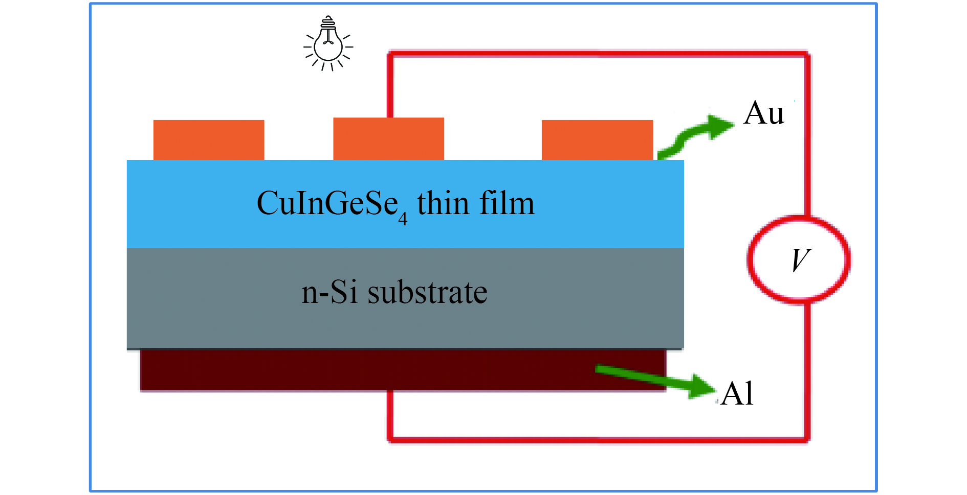
Fig. 1.
(Color online) Schematic diagram of Au/CuInGeSe4/Al heterojunction device.
SEMICONDUCTOR DEVICES
I. M. El Radaf1, A. M. Mansour2, and G. B. Sakr3
Corresponding author: A. M. Mansour, email: amamansour@gmail.com
Abstract: The CuInGeSe4 thin film was deposited onto n-type single crystal silicon wafers by the electron beam deposition technique. The Au/CuInGeSe4/n-Si/Al heterojunction device has been fabricated. The structure of the CuInGeSe4 thin film was characterized by X-ray diffraction (XRD), scanning electron microscope (SEM), and energy dispersive X-ray analysis (EDX). The dark current–voltage characteristics of the Au/CuInGeSe4/n-Si/Al heterojunction diode have been studied at a temperature range of 303–383 K. Also, the photovoltaic properties were examined at different illumination intensities. The capacitance–voltage characteristics of the CuInGeSe4/n-Si heterojunction were studied at different temperatures in the dark.
Keywords: CuInGeSe4, electron beam deposition, series resistance, rectification, ideality factor
| [1] |
Matsushita H, Katsui A. Materials design for Cu-based quaternary compounds derived from chalcopyrite-rule. J Phys Chem Solids, 2005, 66: 1933 doi: 10.1016/j.jpcs.2005.09.028
|
| [2] |
Gorgut G P, Fedorchuk A O, Kityk I V, et al. Synthesis and structural properties of CuInGeS4. J Cryst Growth, 2011, 324: 212 doi: 10.1016/j.jcrysgro.2011.02.029
|
| [3] |
Li W, Yan X, Xu W L, et al. Efficiency improvement of CIGS solar cells by a modified rear contact. Sol Energy, 2017, 157: 486 doi: 10.1016/j.solener.2017.08.054
|
| [4] |
Shah A V, Schade H, Vanecek M, et al. Thin-film silicon solar cell technology. Prog Photovoltaics Res Appl, 2004, 12: 113 doi: 10.1002/pip.533
|
| [5] |
Matsushita H, Ochiai T, Mikajiri K, et al. Preparation of CuInGeSe4 thin films by selenization method using the Cu–In–Ge evaporated layer precursors. J Phys Chem Solids, 2005, 66: 1937 doi: 10.1016/j.jpcs.2005.09.031
|
| [6] |
Matsushita H, Maeda T, Katsui A, et al. Thermal analysis and synthesis from the melts of Cu-based quaternary compounds Cu–III–IV–VI4 and Cu2–II–IV–VI4(II = Zn, Cd; III = Ga, In; IV = Ge, Sn; VI = Se). J Cryst Growth, 2000, 208: 416 doi: 10.1016/S0022-0248(99)00468-6
|
| [7] |
Hughes O H, Woolley J C, Lopez-Rivera S A, et al. Quaternary adamantine selenides and tellurides of the form I III IV VI4. Solid State Commun, 1980, 35: 573 doi: 10.1016/0038-1098(80)90585-2
|
| [8] |
Contreras M A, Ramanathan K, Abushama J, et al. Diode characteristics in state-of-the-art ZnO/CdS/ Cu(In1-xGax)Se2 solar cells. Prog Photovolt Res Appl, 2005, 13: 209 doi: 10.1002/pip.626
|
| [9] |
Abd El-Rahman K F, Darwish A A A, El-Shazly E A A. Electrical and photovoltaic properties of SnSe/Si heterojunction. Mater Sci Semicond Process, 2014, 25: 123 doi: 10.1016/j.mssp.2013.10.003
|
| [10] |
Lin Y, Chen X. Advanced nano deposition methods. Weinheim: Wiley-VCH Verlag GmbH & Co. KGaA, 2016
|
| [11] |
Cuomo J J, Rossnagel S M, Haufman H R, et al. Handbook of ion beam processing technology: principles, deposition, film modification, and synthesis. Westwood: Noyes Publications, 1989
|
| [12] |
Cividjian N, Hagen C W. Electron-beam-induced nanometer-scale deposition. Adv Imaging Electron Phys, 2006, 143: 1 doi: 10.1016/S1076-5670(06)43001-9
|
| [13] |
Strehl P. Beam Instrumentation and Diagnostics. Berlin: Springer, 2006
|
| [14] |
El Radaf I M, Nasr M, Mansour A M. Structural, electrical and photovoltaic properties of CoS/Si heterojunction prepared by spray pyrolysis. Mater Res Express, 2018, 5: 015904 doi: 10.1088/2053-1591/aaa25e
|
| [15] |
Hassan N, Mansour A M, Roushdy N, et al. Optical sensing performance characteristics of Schottky devices diodes based nano-particle disodium 6-hydroxy-5-[(2-methoxy-5-methyl-4-sulfophenyl)azo]-2-naphthalenesulfonate thin films: A comparison study. Optik (Stuttg), 2018, 158: 1255 doi: 10.1016/j.ijleo.2017.12.203
|
| [16] |
Nasr M, El Radaf I M, Mansour A M. Current transport and capacitance–voltage characteristics of an n-PbTe/p-GaP heterojunction prepared using the electron beam deposition technique. J Phys Chem Solids, 2018, 115: 283 doi: 10.1016/j.jpcs.2017.12.029
|
| [17] |
Farag A A M, Terra F S, Mahmoud G M, et al. Study of Gaussian distribution of inhomogeneous barrier height for n-InSb/p-GaAs heterojunction prepared by flash evaporation. J Alloys Compd, 2009, 481: 427 doi: 10.1016/j.jallcom.2009.03.004
|
| [18] |
Farag A A M, Soliman H S, Atta A A. Analysis of dark and photovoltaic characteristics of Au/Pyronine G(Y)/p-Si/Al heterojunction. Synth Met, 2012, 161: 2759 doi: 10.1016/j.synthmet.2011.10.017
|
| [19] |
Farag A A M, Terra F S, Fahim G M M, et al. Current transport and capacitance-voltage characteristics of n-InSb/p-GaP prepared by flash evaporation and liquid phase epitaxy. Met Mater Int, 2012, 18: 509 doi: 10.1007/s12540-012-3020-4
|
| [20] |
Gupta R K, Aydın M E, Yakuphanoglu F. Photoconducting and electrical properties of Al/TIPS-pentacene/p-Si/Al hybrid diode for optical sensor applications. Synth Met, 2011, 161: 2355 doi: 10.1016/j.synthmet.2011.09.002
|
| [21] |
Yahia I S, Farag A A M, Yakuphanoglu F, et al. Temperature dependence of electronic parameters of organic Schottky diode based on fluorescein sodium salt. Synth Met, 2011, 161: 881 doi: 10.1016/j.synthmet.2011.02.016
|
| [22] |
Yahia I S, Fadel M, Sakr G B, et al. Analysis of current–voltage characteristics of Al/p-ZnGa2Se4/n-Si nanocrystalline heterojunction diode. J Alloys Compd, 2011, 509: 4414 doi: 10.1016/j.jallcom.2011.01.068
|
| [23] |
Soliman H S, Farag A A M, Khosifan N M, et al. Electronic and photovoltaic properties of Au/pyronine G(Y)/p-GaAs/Au:Zn heterojunction. J Alloys Compd, 2012, 530: 157 doi: 10.1016/j.jallcom.2012.03.053
|
| [24] |
Çetinkaya H G, Tecimer H, Uslu H, et al. Photovoltaic characteristics of Au/PVA (Bi-doped)/n-Si Schottky barrier diodes (SBDs) at various temperatures. Curr Appl Phys, 2013, 13: 1150 doi: 10.1016/j.cap.2013.03.010
|
| [25] |
Farag A A M, Terra F S, Ashery A, et al. Structural and electrical characteristics of n-InSb/p-GaAs heterojunction prepared by liquid phase epitaxy. J Alloys Compd, 2014, 615: 604 doi: 10.1016/j.jallcom.2014.06.058
|
| [26] |
Farag A A M, Terra F S, Ashery A, et al. Structural and electrical characterization of n-InAs/p-GaP heterojunctions prepared by vacuum flash evaporation and liquid phase epitaxy. Optoelectron. Adv Mater – RAPID Commun, 2017, 11: 82
|
| [27] |
Ahmad Z, Sayyad M H, Yaseen M, et al. Investigation of 5,10,15,20-Tetrakis(3-,5--Di-Tert-Butylphenyl)Porphyrinatocopper(II) for Electronics Applications. Int J Chem Mol Nucl Mater Metall Eng, 2011, 5: 380
|
| [28] |
Farag A A M, Terra F S, Ashery A, et al. Temperature dependence of J-V and C-V characteristics of n-InAs/p-GaAs heterojunctions prepared by flash evaporation technique and liquid phase epitaxy. Indian Pure Appl Phys, 2018, 56: 203
|
| [29] |
El-Nahass M M, Metwally H S, El-Sayed H E A , et al. Electrical and photovoltaic properties of FeTPPCl/p-Si heterojunction. Synth Met, 2011, 161: 2253 doi: 10.1016/j.synthmet.2011.08.030
|
| [30] |
Hameed T A, El Radaf I M, Elsayed-Ali H E. Characterization of CuInGeSe4 thin films and Al/n-Si/p-CuInGeSe4/Au heterojunction device. J Mater Sci Mater Electron, 2018, 29: 12584 doi: 10.1007/s10854-018-9375-7
|
| [31] |
Sze S M, Ng K K. Physics of semiconductor devices. New York: Wiley-Interscience, 2007
|
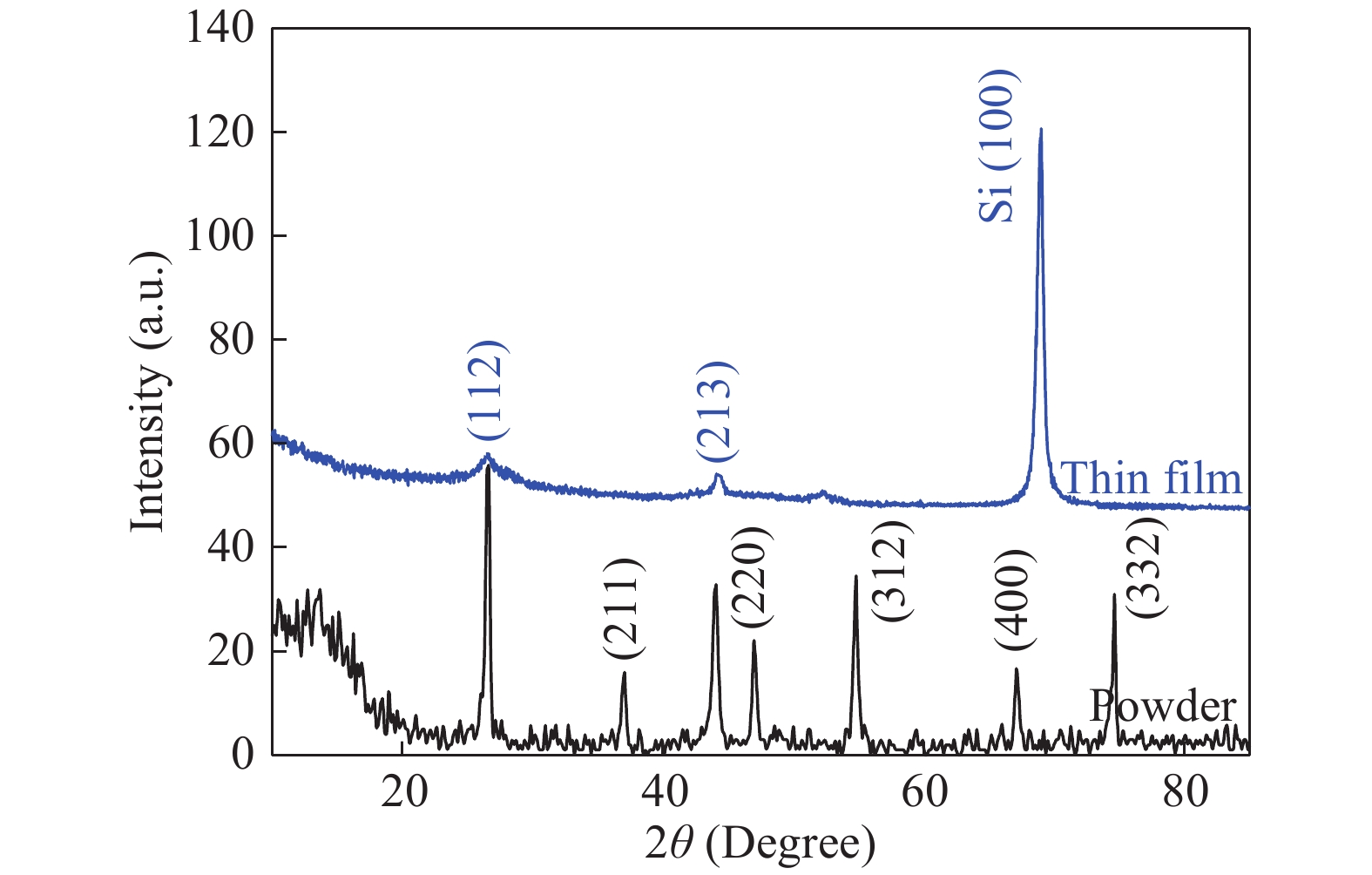
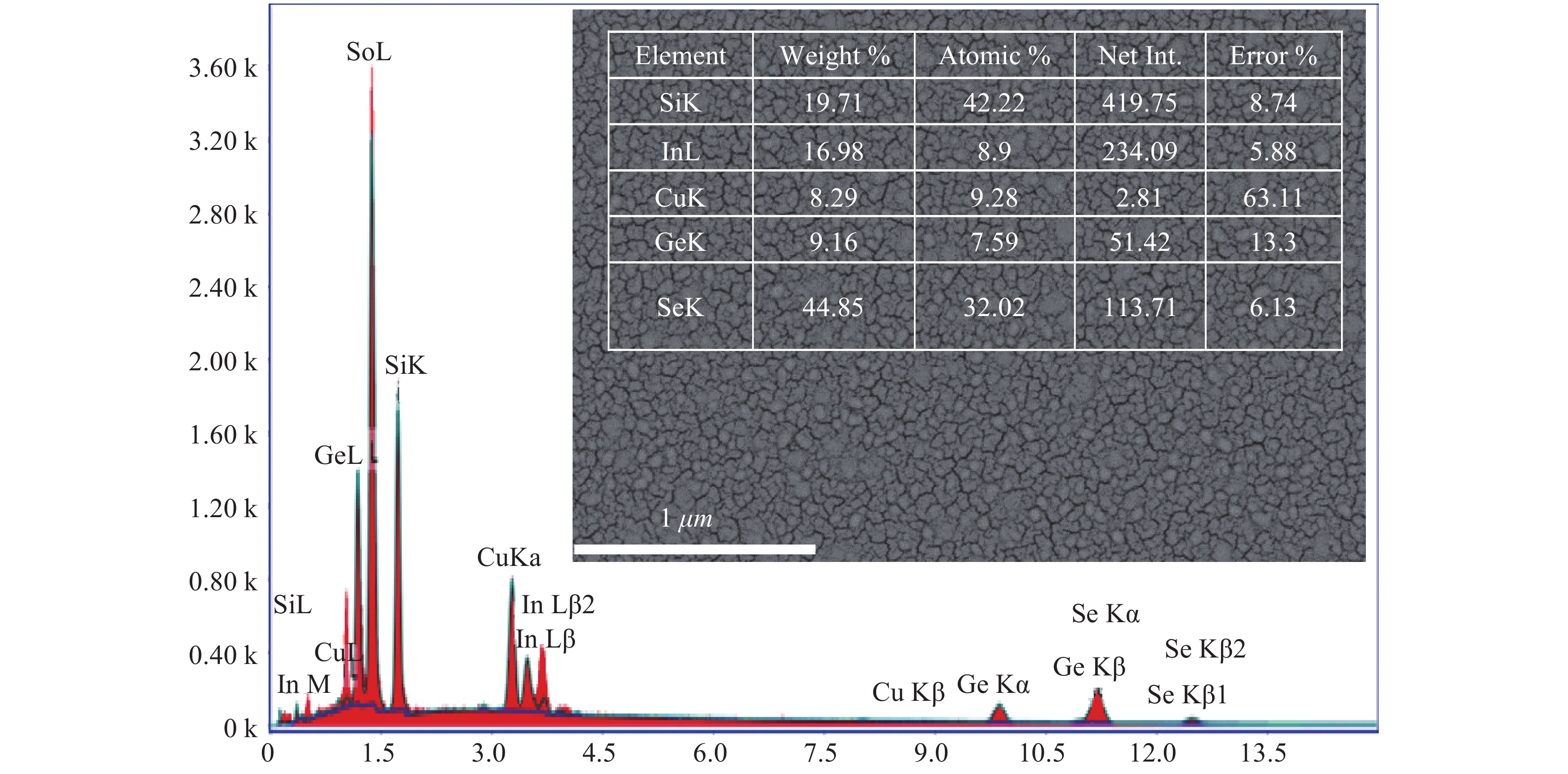
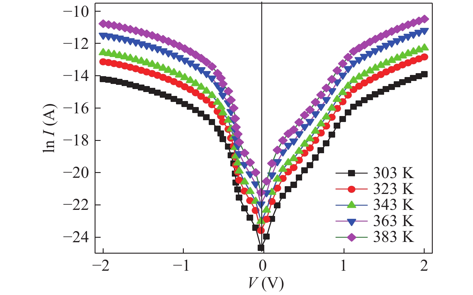
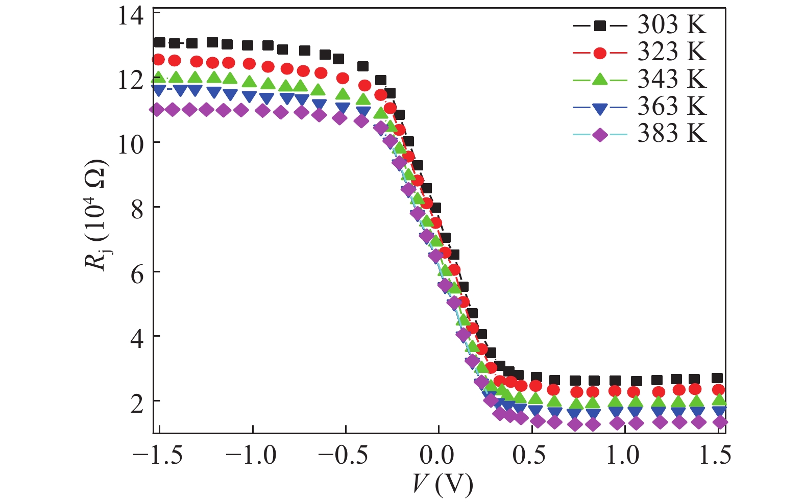
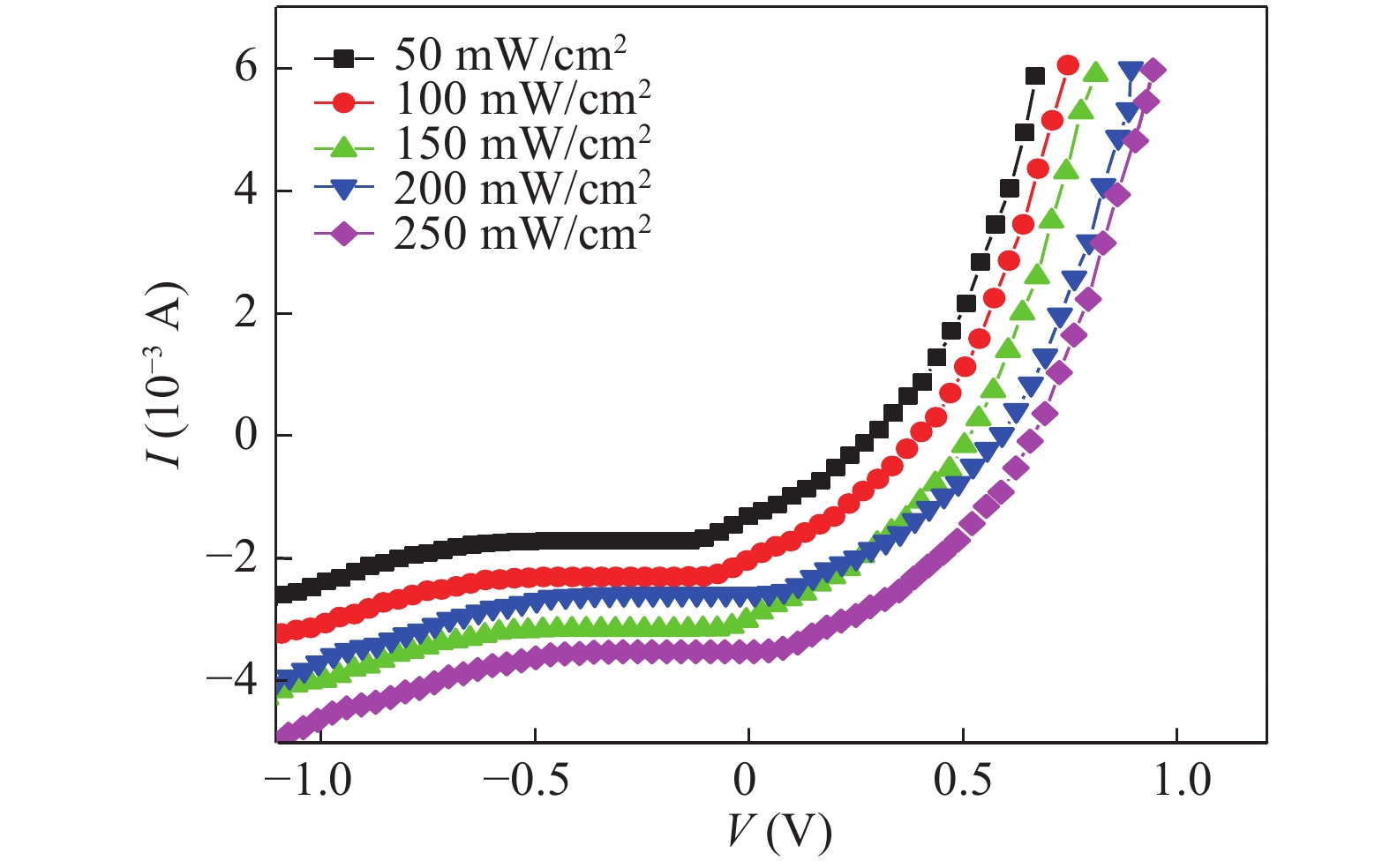
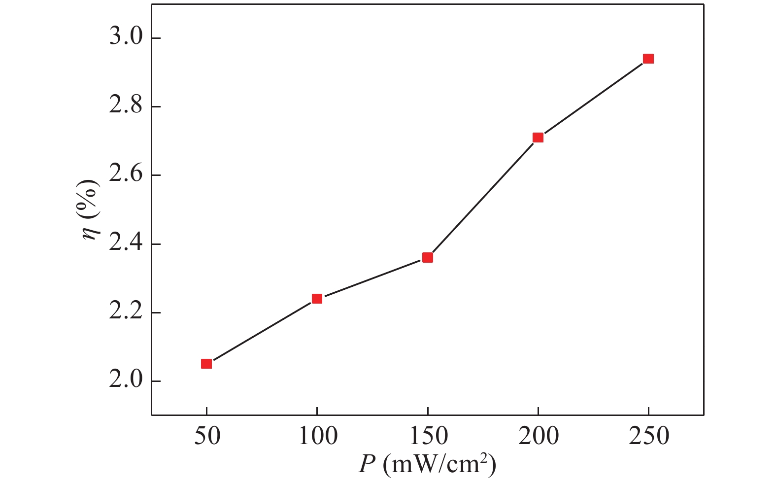
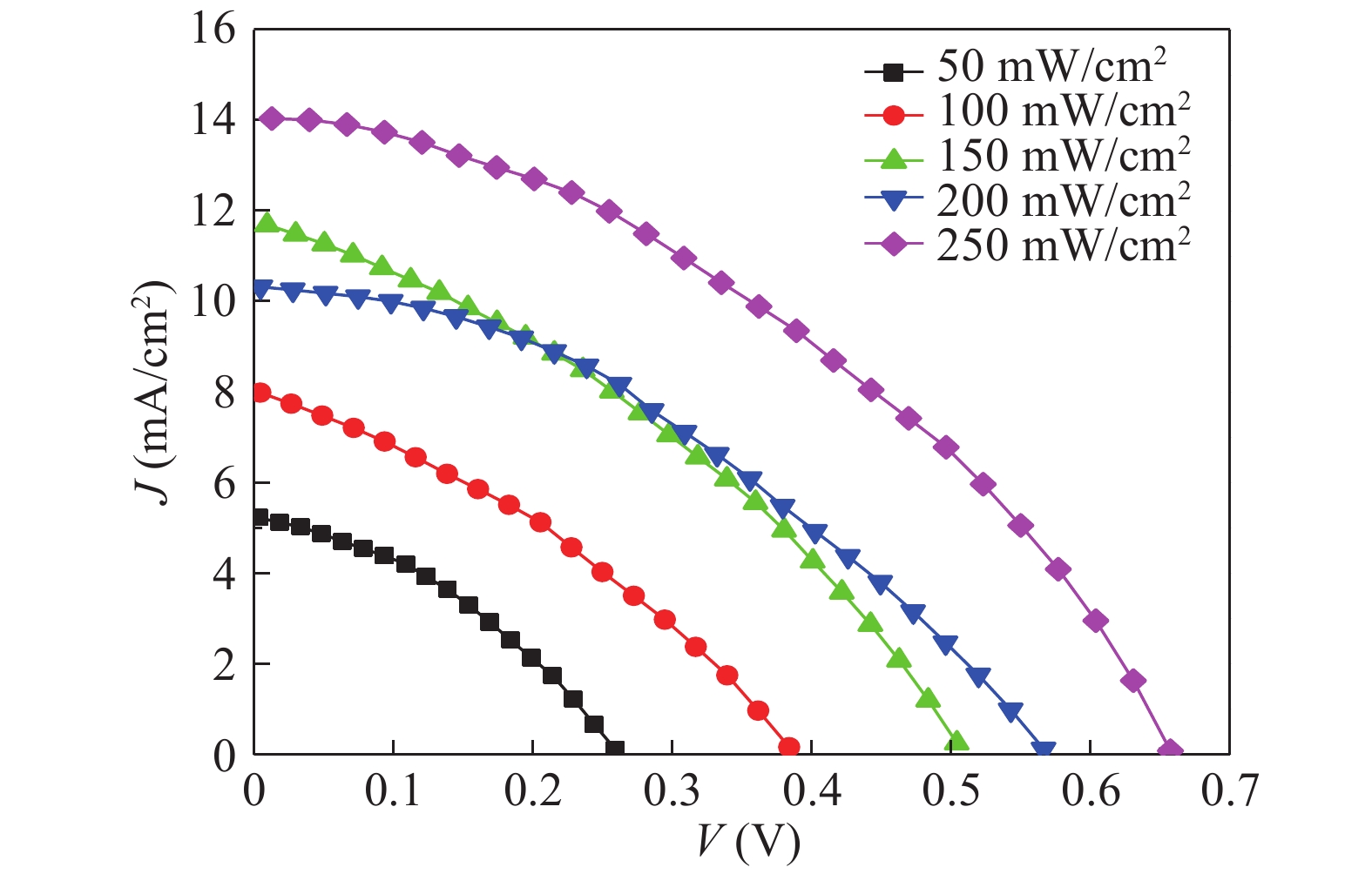
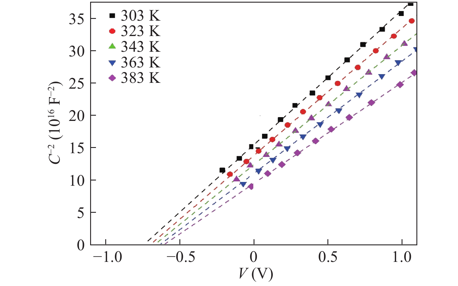
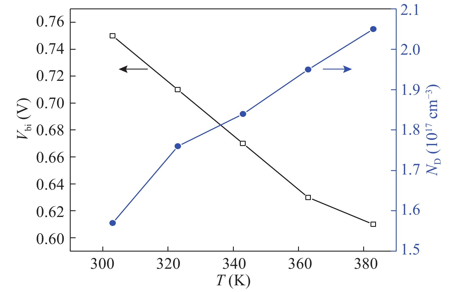
Table 1. Junction parameters determined from the dark I–V characteristics of Au/CuInGeSe4/n-Si/Al heterojunction.
| T (K) | RR (at ±1) | n | RS (kΩ) | Rsh (kΩ) | ϕb (eV) |
| 303 | 94.21 | 2.76 | 2.51 | 132 | 0.53 |
| 323 | 90.52 | 2.59 | 2.13 | 125 | 0.58 |
| 343 | 87.17 | 2.38 | 1.75 | 119 | 0.62 |
| 363 | 81.45 | 2.19 | 1.48 | 115 | 0.68 |
| 383 | 74.96 | 1.95 | 1.12 | 111 | 0.71 |
 DownLoad: CSV
Table 2. The solar parameters determined from the J–V curve of Au/CuInGeSe4/n-Si/Al heterojunction.
| Intensity (mW/cm2) | JSC | VOC | JM | VM | FF | η (%) |
| 50 | 5.26 | 0.26 | 3.42 | 0.15 | 0.37 | 2.05 |
| 100 | 7.98 | 0.38 | 4.97 | 0.21 | 0.39 | 2.24 |
| 150 | 10.24 | 0.51 | 6.81 | 0.31 | 0.41 | 2.36 |
| 200 | 11.75 | 0.62 | 7.22 | 0.32 | 0.38 | 2.71 |
| 250 | 14.12 | 0.65 | 9.14 | 0.41 | 0.40 | 2.94 |
DownLoad: CSV
Table 3. Temperature dependent values of parameters determined from C–V characteristics of Au/CuInGeSe4/n-Si/Al heterojunction.
| T (K) | Vbi (V) | ND (1017 cm−3) |
| 303 | 0.75 | 1.57 |
| 323 | 0.71 | 1.76 |
| 343 | 0.67 | 1.84 |
| 363 | 0.63 | 1.95 |
| 383 | 0.61 | 2.05 |
DownLoad: CSV
| [1] |
Matsushita H, Katsui A. Materials design for Cu-based quaternary compounds derived from chalcopyrite-rule. J Phys Chem Solids, 2005, 66: 1933 doi: 10.1016/j.jpcs.2005.09.028
|
| [2] |
Gorgut G P, Fedorchuk A O, Kityk I V, et al. Synthesis and structural properties of CuInGeS4. J Cryst Growth, 2011, 324: 212 doi: 10.1016/j.jcrysgro.2011.02.029
|
| [3] |
Li W, Yan X, Xu W L, et al. Efficiency improvement of CIGS solar cells by a modified rear contact. Sol Energy, 2017, 157: 486 doi: 10.1016/j.solener.2017.08.054
|
| [4] |
Shah A V, Schade H, Vanecek M, et al. Thin-film silicon solar cell technology. Prog Photovoltaics Res Appl, 2004, 12: 113 doi: 10.1002/pip.533
|
| [5] |
Matsushita H, Ochiai T, Mikajiri K, et al. Preparation of CuInGeSe4 thin films by selenization method using the Cu–In–Ge evaporated layer precursors. J Phys Chem Solids, 2005, 66: 1937 doi: 10.1016/j.jpcs.2005.09.031
|
| [6] |
Matsushita H, Maeda T, Katsui A, et al. Thermal analysis and synthesis from the melts of Cu-based quaternary compounds Cu–III–IV–VI4 and Cu2–II–IV–VI4(II = Zn, Cd; III = Ga, In; IV = Ge, Sn; VI = Se). J Cryst Growth, 2000, 208: 416 doi: 10.1016/S0022-0248(99)00468-6
|
| [7] |
Hughes O H, Woolley J C, Lopez-Rivera S A, et al. Quaternary adamantine selenides and tellurides of the form I III IV VI4. Solid State Commun, 1980, 35: 573 doi: 10.1016/0038-1098(80)90585-2
|
| [8] |
Contreras M A, Ramanathan K, Abushama J, et al. Diode characteristics in state-of-the-art ZnO/CdS/ Cu(In1-xGax)Se2 solar cells. Prog Photovolt Res Appl, 2005, 13: 209 doi: 10.1002/pip.626
|
| [9] |
Abd El-Rahman K F, Darwish A A A, El-Shazly E A A. Electrical and photovoltaic properties of SnSe/Si heterojunction. Mater Sci Semicond Process, 2014, 25: 123 doi: 10.1016/j.mssp.2013.10.003
|
| [10] |
Lin Y, Chen X. Advanced nano deposition methods. Weinheim: Wiley-VCH Verlag GmbH & Co. KGaA, 2016
|
| [11] |
Cuomo J J, Rossnagel S M, Haufman H R, et al. Handbook of ion beam processing technology: principles, deposition, film modification, and synthesis. Westwood: Noyes Publications, 1989
|
| [12] |
Cividjian N, Hagen C W. Electron-beam-induced nanometer-scale deposition. Adv Imaging Electron Phys, 2006, 143: 1 doi: 10.1016/S1076-5670(06)43001-9
|
| [13] |
Strehl P. Beam Instrumentation and Diagnostics. Berlin: Springer, 2006
|
| [14] |
El Radaf I M, Nasr M, Mansour A M. Structural, electrical and photovoltaic properties of CoS/Si heterojunction prepared by spray pyrolysis. Mater Res Express, 2018, 5: 015904 doi: 10.1088/2053-1591/aaa25e
|
| [15] |
Hassan N, Mansour A M, Roushdy N, et al. Optical sensing performance characteristics of Schottky devices diodes based nano-particle disodium 6-hydroxy-5-[(2-methoxy-5-methyl-4-sulfophenyl)azo]-2-naphthalenesulfonate thin films: A comparison study. Optik (Stuttg), 2018, 158: 1255 doi: 10.1016/j.ijleo.2017.12.203
|
| [16] |
Nasr M, El Radaf I M, Mansour A M. Current transport and capacitance–voltage characteristics of an n-PbTe/p-GaP heterojunction prepared using the electron beam deposition technique. J Phys Chem Solids, 2018, 115: 283 doi: 10.1016/j.jpcs.2017.12.029
|
| [17] |
Farag A A M, Terra F S, Mahmoud G M, et al. Study of Gaussian distribution of inhomogeneous barrier height for n-InSb/p-GaAs heterojunction prepared by flash evaporation. J Alloys Compd, 2009, 481: 427 doi: 10.1016/j.jallcom.2009.03.004
|
| [18] |
Farag A A M, Soliman H S, Atta A A. Analysis of dark and photovoltaic characteristics of Au/Pyronine G(Y)/p-Si/Al heterojunction. Synth Met, 2012, 161: 2759 doi: 10.1016/j.synthmet.2011.10.017
|
| [19] |
Farag A A M, Terra F S, Fahim G M M, et al. Current transport and capacitance-voltage characteristics of n-InSb/p-GaP prepared by flash evaporation and liquid phase epitaxy. Met Mater Int, 2012, 18: 509 doi: 10.1007/s12540-012-3020-4
|
| [20] |
Gupta R K, Aydın M E, Yakuphanoglu F. Photoconducting and electrical properties of Al/TIPS-pentacene/p-Si/Al hybrid diode for optical sensor applications. Synth Met, 2011, 161: 2355 doi: 10.1016/j.synthmet.2011.09.002
|
| [21] |
Yahia I S, Farag A A M, Yakuphanoglu F, et al. Temperature dependence of electronic parameters of organic Schottky diode based on fluorescein sodium salt. Synth Met, 2011, 161: 881 doi: 10.1016/j.synthmet.2011.02.016
|
| [22] |
Yahia I S, Fadel M, Sakr G B, et al. Analysis of current–voltage characteristics of Al/p-ZnGa2Se4/n-Si nanocrystalline heterojunction diode. J Alloys Compd, 2011, 509: 4414 doi: 10.1016/j.jallcom.2011.01.068
|
| [23] |
Soliman H S, Farag A A M, Khosifan N M, et al. Electronic and photovoltaic properties of Au/pyronine G(Y)/p-GaAs/Au:Zn heterojunction. J Alloys Compd, 2012, 530: 157 doi: 10.1016/j.jallcom.2012.03.053
|
| [24] |
Çetinkaya H G, Tecimer H, Uslu H, et al. Photovoltaic characteristics of Au/PVA (Bi-doped)/n-Si Schottky barrier diodes (SBDs) at various temperatures. Curr Appl Phys, 2013, 13: 1150 doi: 10.1016/j.cap.2013.03.010
|
| [25] |
Farag A A M, Terra F S, Ashery A, et al. Structural and electrical characteristics of n-InSb/p-GaAs heterojunction prepared by liquid phase epitaxy. J Alloys Compd, 2014, 615: 604 doi: 10.1016/j.jallcom.2014.06.058
|
| [26] |
Farag A A M, Terra F S, Ashery A, et al. Structural and electrical characterization of n-InAs/p-GaP heterojunctions prepared by vacuum flash evaporation and liquid phase epitaxy. Optoelectron. Adv Mater – RAPID Commun, 2017, 11: 82
|
| [27] |
Ahmad Z, Sayyad M H, Yaseen M, et al. Investigation of 5,10,15,20-Tetrakis(3-,5--Di-Tert-Butylphenyl)Porphyrinatocopper(II) for Electronics Applications. Int J Chem Mol Nucl Mater Metall Eng, 2011, 5: 380
|
| [28] |
Farag A A M, Terra F S, Ashery A, et al. Temperature dependence of J-V and C-V characteristics of n-InAs/p-GaAs heterojunctions prepared by flash evaporation technique and liquid phase epitaxy. Indian Pure Appl Phys, 2018, 56: 203
|
| [29] |
El-Nahass M M, Metwally H S, El-Sayed H E A , et al. Electrical and photovoltaic properties of FeTPPCl/p-Si heterojunction. Synth Met, 2011, 161: 2253 doi: 10.1016/j.synthmet.2011.08.030
|
| [30] |
Hameed T A, El Radaf I M, Elsayed-Ali H E. Characterization of CuInGeSe4 thin films and Al/n-Si/p-CuInGeSe4/Au heterojunction device. J Mater Sci Mater Electron, 2018, 29: 12584 doi: 10.1007/s10854-018-9375-7
|
| [31] |
Sze S M, Ng K K. Physics of semiconductor devices. New York: Wiley-Interscience, 2007
|


Article views: 4351 Times PDF downloads: 54 Times Cited by: 0 Times
Received: 11 May 2018 Revised: 17 June 2018 Online: Uncorrected proof: 13 September 2018Published: 13 December 2018
| Citation: |
I. M. El Radaf, A. M. Mansour, G. B. Sakr. Fabrication, electrical and photovoltaic characteristics of CuInGeSe4/n-Si diode[J]. Journal of Semiconductors, 2018, 39(12): 124010. doi: 10.1088/1674-4926/39/12/124010
****
I M El Radaf, A M Mansour, G B Sakr, Fabrication, electrical and photovoltaic characteristics of CuInGeSe4/n-Si diode[J]. J. Semicond., 2018, 39(12): 124010. doi: 10.1088/1674-4926/39/12/124010.

|
| [1] |
Matsushita H, Katsui A. Materials design for Cu-based quaternary compounds derived from chalcopyrite-rule. J Phys Chem Solids, 2005, 66: 1933 doi: 10.1016/j.jpcs.2005.09.028
|
| [2] |
Gorgut G P, Fedorchuk A O, Kityk I V, et al. Synthesis and structural properties of CuInGeS4. J Cryst Growth, 2011, 324: 212 doi: 10.1016/j.jcrysgro.2011.02.029
|
| [3] |
Li W, Yan X, Xu W L, et al. Efficiency improvement of CIGS solar cells by a modified rear contact. Sol Energy, 2017, 157: 486 doi: 10.1016/j.solener.2017.08.054
|
| [4] |
Shah A V, Schade H, Vanecek M, et al. Thin-film silicon solar cell technology. Prog Photovoltaics Res Appl, 2004, 12: 113 doi: 10.1002/pip.533
|
| [5] |
Matsushita H, Ochiai T, Mikajiri K, et al. Preparation of CuInGeSe4 thin films by selenization method using the Cu–In–Ge evaporated layer precursors. J Phys Chem Solids, 2005, 66: 1937 doi: 10.1016/j.jpcs.2005.09.031
|
| [6] |
Matsushita H, Maeda T, Katsui A, et al. Thermal analysis and synthesis from the melts of Cu-based quaternary compounds Cu–III–IV–VI4 and Cu2–II–IV–VI4(II = Zn, Cd; III = Ga, In; IV = Ge, Sn; VI = Se). J Cryst Growth, 2000, 208: 416 doi: 10.1016/S0022-0248(99)00468-6
|
| [7] |
Hughes O H, Woolley J C, Lopez-Rivera S A, et al. Quaternary adamantine selenides and tellurides of the form I III IV VI4. Solid State Commun, 1980, 35: 573 doi: 10.1016/0038-1098(80)90585-2
|
| [8] |
Contreras M A, Ramanathan K, Abushama J, et al. Diode characteristics in state-of-the-art ZnO/CdS/ Cu(In1-xGax)Se2 solar cells. Prog Photovolt Res Appl, 2005, 13: 209 doi: 10.1002/pip.626
|
| [9] |
Abd El-Rahman K F, Darwish A A A, El-Shazly E A A. Electrical and photovoltaic properties of SnSe/Si heterojunction. Mater Sci Semicond Process, 2014, 25: 123 doi: 10.1016/j.mssp.2013.10.003
|
| [10] |
Lin Y, Chen X. Advanced nano deposition methods. Weinheim: Wiley-VCH Verlag GmbH & Co. KGaA, 2016
|
| [11] |
Cuomo J J, Rossnagel S M, Haufman H R, et al. Handbook of ion beam processing technology: principles, deposition, film modification, and synthesis. Westwood: Noyes Publications, 1989
|
| [12] |
Cividjian N, Hagen C W. Electron-beam-induced nanometer-scale deposition. Adv Imaging Electron Phys, 2006, 143: 1 doi: 10.1016/S1076-5670(06)43001-9
|
| [13] |
Strehl P. Beam Instrumentation and Diagnostics. Berlin: Springer, 2006
|
| [14] |
El Radaf I M, Nasr M, Mansour A M. Structural, electrical and photovoltaic properties of CoS/Si heterojunction prepared by spray pyrolysis. Mater Res Express, 2018, 5: 015904 doi: 10.1088/2053-1591/aaa25e
|
| [15] |
Hassan N, Mansour A M, Roushdy N, et al. Optical sensing performance characteristics of Schottky devices diodes based nano-particle disodium 6-hydroxy-5-[(2-methoxy-5-methyl-4-sulfophenyl)azo]-2-naphthalenesulfonate thin films: A comparison study. Optik (Stuttg), 2018, 158: 1255 doi: 10.1016/j.ijleo.2017.12.203
|
| [16] |
Nasr M, El Radaf I M, Mansour A M. Current transport and capacitance–voltage characteristics of an n-PbTe/p-GaP heterojunction prepared using the electron beam deposition technique. J Phys Chem Solids, 2018, 115: 283 doi: 10.1016/j.jpcs.2017.12.029
|
| [17] |
Farag A A M, Terra F S, Mahmoud G M, et al. Study of Gaussian distribution of inhomogeneous barrier height for n-InSb/p-GaAs heterojunction prepared by flash evaporation. J Alloys Compd, 2009, 481: 427 doi: 10.1016/j.jallcom.2009.03.004
|
| [18] |
Farag A A M, Soliman H S, Atta A A. Analysis of dark and photovoltaic characteristics of Au/Pyronine G(Y)/p-Si/Al heterojunction. Synth Met, 2012, 161: 2759 doi: 10.1016/j.synthmet.2011.10.017
|
| [19] |
Farag A A M, Terra F S, Fahim G M M, et al. Current transport and capacitance-voltage characteristics of n-InSb/p-GaP prepared by flash evaporation and liquid phase epitaxy. Met Mater Int, 2012, 18: 509 doi: 10.1007/s12540-012-3020-4
|
| [20] |
Gupta R K, Aydın M E, Yakuphanoglu F. Photoconducting and electrical properties of Al/TIPS-pentacene/p-Si/Al hybrid diode for optical sensor applications. Synth Met, 2011, 161: 2355 doi: 10.1016/j.synthmet.2011.09.002
|
| [21] |
Yahia I S, Farag A A M, Yakuphanoglu F, et al. Temperature dependence of electronic parameters of organic Schottky diode based on fluorescein sodium salt. Synth Met, 2011, 161: 881 doi: 10.1016/j.synthmet.2011.02.016
|
| [22] |
Yahia I S, Fadel M, Sakr G B, et al. Analysis of current–voltage characteristics of Al/p-ZnGa2Se4/n-Si nanocrystalline heterojunction diode. J Alloys Compd, 2011, 509: 4414 doi: 10.1016/j.jallcom.2011.01.068
|
| [23] |
Soliman H S, Farag A A M, Khosifan N M, et al. Electronic and photovoltaic properties of Au/pyronine G(Y)/p-GaAs/Au:Zn heterojunction. J Alloys Compd, 2012, 530: 157 doi: 10.1016/j.jallcom.2012.03.053
|
| [24] |
Çetinkaya H G, Tecimer H, Uslu H, et al. Photovoltaic characteristics of Au/PVA (Bi-doped)/n-Si Schottky barrier diodes (SBDs) at various temperatures. Curr Appl Phys, 2013, 13: 1150 doi: 10.1016/j.cap.2013.03.010
|
| [25] |
Farag A A M, Terra F S, Ashery A, et al. Structural and electrical characteristics of n-InSb/p-GaAs heterojunction prepared by liquid phase epitaxy. J Alloys Compd, 2014, 615: 604 doi: 10.1016/j.jallcom.2014.06.058
|
| [26] |
Farag A A M, Terra F S, Ashery A, et al. Structural and electrical characterization of n-InAs/p-GaP heterojunctions prepared by vacuum flash evaporation and liquid phase epitaxy. Optoelectron. Adv Mater – RAPID Commun, 2017, 11: 82
|
| [27] |
Ahmad Z, Sayyad M H, Yaseen M, et al. Investigation of 5,10,15,20-Tetrakis(3-,5--Di-Tert-Butylphenyl)Porphyrinatocopper(II) for Electronics Applications. Int J Chem Mol Nucl Mater Metall Eng, 2011, 5: 380
|
| [28] |
Farag A A M, Terra F S, Ashery A, et al. Temperature dependence of J-V and C-V characteristics of n-InAs/p-GaAs heterojunctions prepared by flash evaporation technique and liquid phase epitaxy. Indian Pure Appl Phys, 2018, 56: 203
|
| [29] |
El-Nahass M M, Metwally H S, El-Sayed H E A , et al. Electrical and photovoltaic properties of FeTPPCl/p-Si heterojunction. Synth Met, 2011, 161: 2253 doi: 10.1016/j.synthmet.2011.08.030
|
| [30] |
Hameed T A, El Radaf I M, Elsayed-Ali H E. Characterization of CuInGeSe4 thin films and Al/n-Si/p-CuInGeSe4/Au heterojunction device. J Mater Sci Mater Electron, 2018, 29: 12584 doi: 10.1007/s10854-018-9375-7
|
| [31] |
Sze S M, Ng K K. Physics of semiconductor devices. New York: Wiley-Interscience, 2007
|

 WeChat ID
Journal of Semiconductors © 2017 All Rights Reserved 京ICP备05085259号-2


