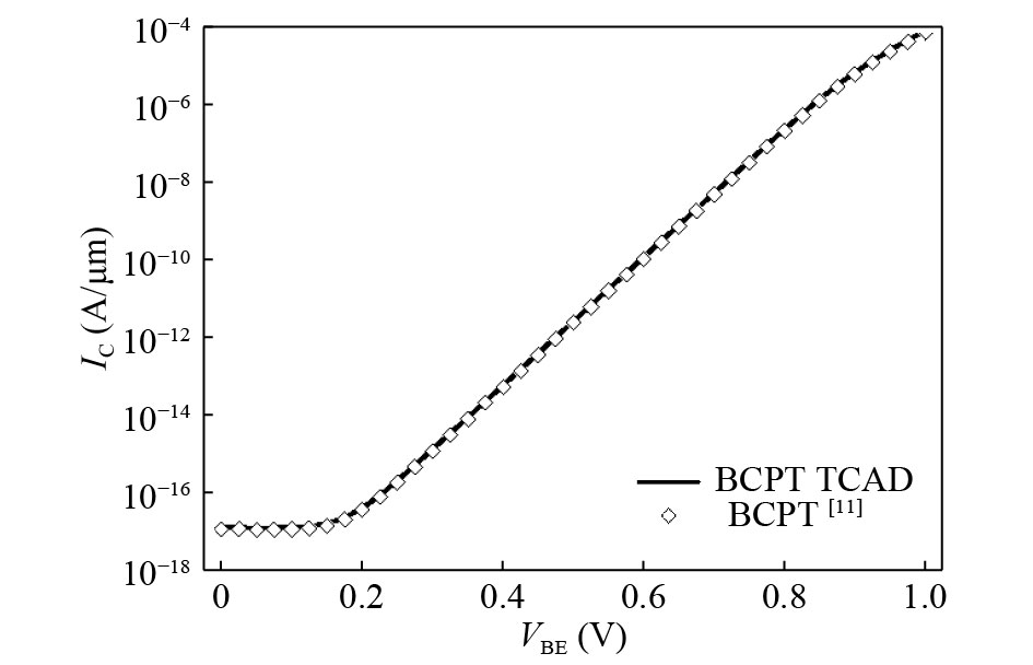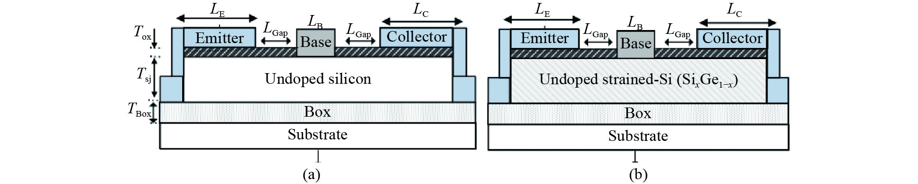
Fig. 1.
(Color online) Schematic diagrams of (a) conventional BCPT, and (b) proposed strained BCPT device.
SEMICONDUCTOR DEVICES
Corresponding author: Sangeeta Singh, Email: sangeeta@iiitkota.ac.in, sangeetasingh.1409@gmail.com
Abstract: In this manuscript we analyze a unique approach to improve the performance of the bipolar charge plasma transistor (BCPT) by introducing a strained Si/SixGe1−x layer as the active device region. For charge plasma realization different metal work-function electrodes are used to induce n+ and p+ regions on undoped strained silicon-on-insulator (sSOI or SixGe1−x) to realize emitter, base, and collector regions of the BCPT. Here, by using a calibrated 2-D TCAD simulation the impact of a Si mole fraction x (in SixGe1−x) on device performance metrics is investigated. The analysis demonstrates the band gap lowering with decreasing Si content or effective strain on the Si layer, and its subsequent advantages. This work reports a significant improvement in current gain, cutoff frequency, and lower collector breakdown voltage (BVCEO) for the proposed structure over the conventional device. The effect of varying temperature on the strained Si layer and its implications on the device performance is also investigated. The analysis demonstrates a fair device-level understanding and exhibits the immense potential of the SixGe1−x material as the device layer. In addition to this, using extensive 2-D mixed-mode TCAD simulation, a considerable improvement in switching transient times are also observed compared to its conventional counterpart.
Keywords: bipolar charge plasma transistor (BCPT), strained Si layer, mole fraction, band gap lowering, current gain (β), cutoff frequency (fT), collector breakdown voltage (BVCEO)
| [1] |
Rein H M, Moller M. Design considerations for very-high-speed Si-bipolar IC's operating up to 50 Gb/s. IEEE J Solid-State Circuits, 1996, 31(8): 1076 doi: 10.1109/4.508255
|
| [2] |
Harame D L, Ahlgren D C, Coolbaugh D D, et al. Current status and future trends of SiGe BiCMOS technology. IEEE Trans Electron Devices, 2001, 48(11): 2575 doi: 10.1109/16.960385
|
| [3] |
Voegeli B T, Gray P B, Rainey B A, et al. High performance, low complexity vertical PNP BJT integrated in a 0.18 μm SiGe BiCMOS technology. Proceedings of the Bipolar/BiCMOS Circuits and Technology Meeting, 2005: 136
|
| [4] |
Martinez A, Barker J R, Svizhenko A, et al. The impact of random dopant aggregation in source and drain on the performance of ballistic DG nano-MOSFETs: a NEGF study. IEEE Trans Nanotechnol, 2007, 6(4): 438 doi: 10.1109/TNANO.2007.899638
|
| [5] |
Chiang M H, Lin J N, Kim K, et al. Random dopant fluctuation in limited-width FinFET technologies. IEEE Trans Electron Devices, 2007, 54(8): 2055 doi: 10.1109/TED.2007.901154
|
| [6] |
Singh S, Kondekar P N. Dopingless super-steep impact ionisation MOS (dopingless-IMOS) based on work-function engineering. IET Electron Lett, 2014, 50(12): 888 doi: 10.1049/el.2014.1072
|
| [7] |
Singh S, Pal P, Kondekar P N. Charge-plasma-based super-steep negative capacitance junctionless tunnel field effect transistor: design and performance. Electron Lett, 2014, 50(25): 1963 doi: 10.1049/el.2014.3256
|
| [8] |
Singh S, Kondekar P N. A novel dynamically configurable electrostatically doped silicon nanowire impact ionization MOS. Superlattices Microstruct, 2015, 88: 695 doi: 10.1016/j.spmi.2015.10.033
|
| [9] |
Singh S, Sinha R, Kondekar P N. A novel ultra steep dynamically reconfigurable electrostatically doped silicon nanowire Schottky barrier FET. Superlattices Microstruct, 2016, 93: 40 doi: 10.1016/j.spmi.2016.02.039
|
| [10] |
Rajasekharan B, Hueting R J, Salm C, et al. Fabrication and characterization of the charge-plasma diode. IEEE Electron Device Lett, 2010, 31(6): 528 doi: 10.1109/LED.2010.2045731
|
| [11] |
Kumar M J, Nadda K. Bipolar charge-plasma transistor: a novel three terminal device. IEEE Trans Electron Devices, 2012, 59(4): 962 doi: 10.1109/TED.2012.2184763
|
| [12] |
Nadda K, Kumar M J. Schottky collector bipolar transistor without impurity doped emitter and base: design and performance. IEEE Trans Electron Devices, 2013, 60(9): 2956 doi: 10.1109/TED.2013.2272943
|
| [13] |
Nadda K, Kumar M J. Thin-film bipolar transistors on recrystallized polycrystalline silicon without impurity doped junctions: proposal and investigation. J Display Technol, 2014, 10(7): 590 doi: 10.1109/JDT.2014.2310124
|
| [14] |
Nadda K, Kumar M J. Vertical bipolar charge plasma transistor with buried metal layer. Sci Rep, 2015, 5: 7860 doi: 10.1038/srep07860
|
| [15] |
Persson S, Fjer M, Cousin E E, Olsen S H, et al. Strained-silicon heterojunction bipolar transistor. IEEE Trans Electron Devices, 2010, 57(6): 1243 doi: 10.1109/TED.2010.2045667
|
| [16] |
Lu T C, Kuo J B. A closed-form analytical BJT forward transit time model considering bandgap-narrowing effects and concentration-dependent diffusion coefficients. Solid-State Electron, 1992, 35(9): 1374 doi: 10.1016/0038-1101(92)90175-C
|
| [17] |
Behera P, Mohapatra S K. A comparative study on SiGe HBTs and Si BJTs in nanoscale. Int J Adv Sci Technol, 2014, 71: 59 doi: 10.14257/ijast
|
| [18] |
Clifford K, Hoyt J L, Gibbons J F. Bandgap and transport properties of Si1−xGex by analysis of nearly ideal Si/Si1−xGex/Si heterojunction bipolar transistors. IEEE Trans Electron Devices, 1989, 36(10): 2093 doi: 10.1109/16.40925
|
| [19] |
Huang C J, Sun C J, Grotjohn T A, et al. Temperature dependence and post-stress recovery of hot electron degradation effects in bipolar transistors. IEEE Proc Bipolar Circuits and Technology Meeting, 1991: 170
|
| [20] |
Sheng S R, McAlister S P, Storey C, et al. Hot-carrier induced degradation and recovery in polysilicon-emitter bipolar transistors. Solid-State Electron, 2002, 46(10): 1603 doi: 10.1016/S0038-1101(02)00112-0
|
| [21] |
Gurrum S P, Suman S K, Joshi Y K, et al. Thermal issues in next-generation integrated circuits. IEEE Trans Device Mater. Reliab, 2004, 4(4): 709 doi: 10.1109/TDMR.2004.840160
|
| [22] |
Olsson J. Self-heating effects in SOI bipolar transistors. Microelectron Eng, 2001, 56(3): 339
|
| [23] |
Zhang W R, Yang J W, Liu H J, et al. The temperature dependence of DC characteristics and its implication in microwave power Si/SiGe/Si HBTs. 4th IEEE Int Conf on Microwave and Millimeter Wave Technology, 2004: 594
|
| [24] |
Kumar M J, Singh P. A super beta bipolar transistor using SiGe-base surface accumulation layer transistor (SALTran) concept: A simulation study. IEEE Trans Electron Devices, 2006, 53(3): 577 doi: 10.1109/TED.2005.863538
|
| [25] |
Kumar M J, Parihar V. Surface accumulation layer transistor (SALTran): A new bipolar transistor for enhanced current gain and reduced hot-carrier degradation. IEEE Trans Device Mater Reliab, 2004, 4(3): 509 doi: 10.1109/TDMR.2004.829074
|
| [26] |
Prijic Z, Pavlovic Z, Ristic S, Stojadinovic N. Zero-temperature-coefficient (ZTC) biasing of power VDMOS transistors. Electron Lett, 1993, 29(5): 435 doi: 10.1049/el:19930291
|
| [27] |
Sahu P K, Mohapatra S K, Pradhan K P. Zero temperature-coefficient bias point over wide range of temperatures for single- and double-gate UTB-SOI n-MOSFETs with trapped charges. Mater Sci Semicond Process, 2015, 31: 175 doi: 10.1016/j.mssp.2014.11.036
|
| [28] |
Ward R R, Dawson W J, Zhu L, et al. Power diodes for cryogenic operation. IEEE 34th Annual Power Electronics Specialist Conf, 2003, 4: 1891
|
| [29] |
Momose H S, Hiroshi I. Analysis of the temperature dependence of hot-carrier-induced degradation in bipolar transistors for Bi-CMOS. IEEE Trans Electron Devices, 1994, 41(6): 978 doi: 10.1109/16.293311
|
| [30] |
Webster W M. On the variation of junction-transistor current-amplification factor with emitter current. Proc IRE, 1954, 42(6): 914 doi: 10.1109/JRPROC.1954.274751
|
| [31] |
Kirk C T. A theory of transistor cutoff frequency (fT) falloff at high current densities. IRE Trans Electron Devices, 1962, 9(2): 164 doi: 10.1109/T-ED.1962.14965
|
| [32] |
Tsu R, Hernandez J G. Temperature dependence of silicon Raman lines. Appl Phys Lett, 1982, 41(11): 1016 doi: 10.1063/1.93394
|
| [33] |
Hassan M S, Nomani M W. Base-transit-time model considering field dependent mobility for BJTs operating at high-level injection. IEEE Trans Electron Devices, 2006, 53(10): 2532 doi: 10.1109/TED.2006.882269
|
| [34] |
Loan S A, Bashir F, Rafat M, et al. A high performance charge plasma based lateral bipolar transistor on selective buried oxide. Semicond Sci Technol, 2013, 29(1): 015011
|
| [35] |
Zhang Y R, Zhang B, Li Z J, et al. Two-dimensional analysis of the interface state effect on current gain for a 4H-SiC bipolar junction transistor. Chin Phys B, 2010, 19(6): 067102 doi: 10.1088/1674-1056/19/6/067102
|
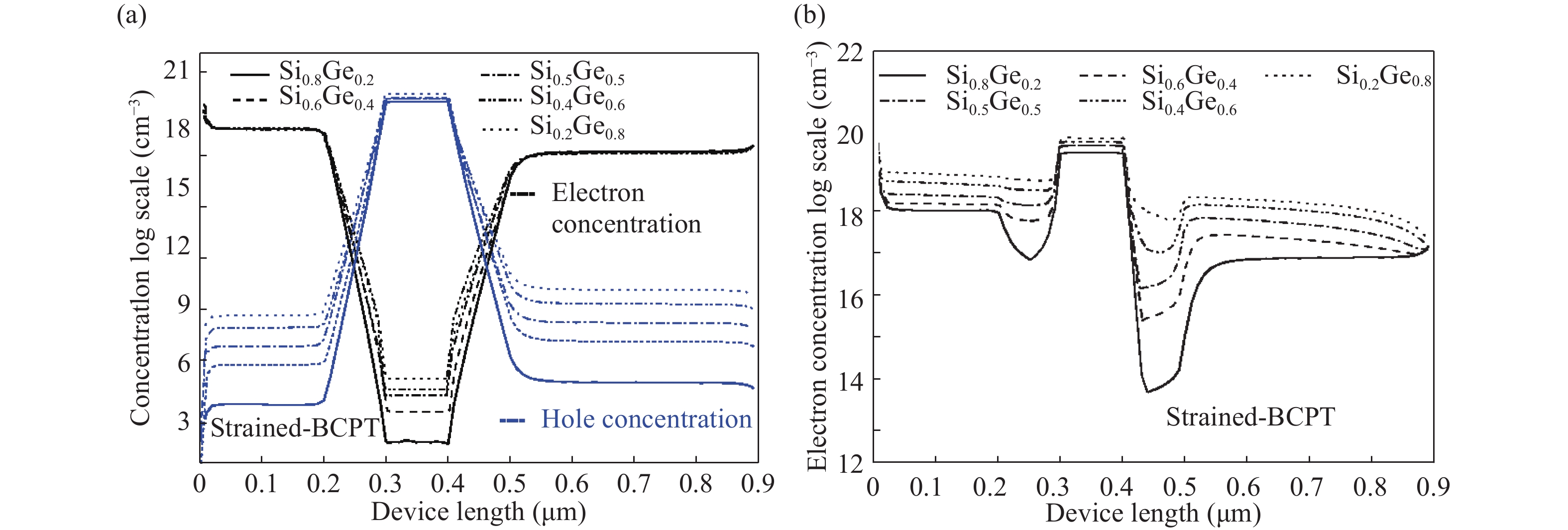
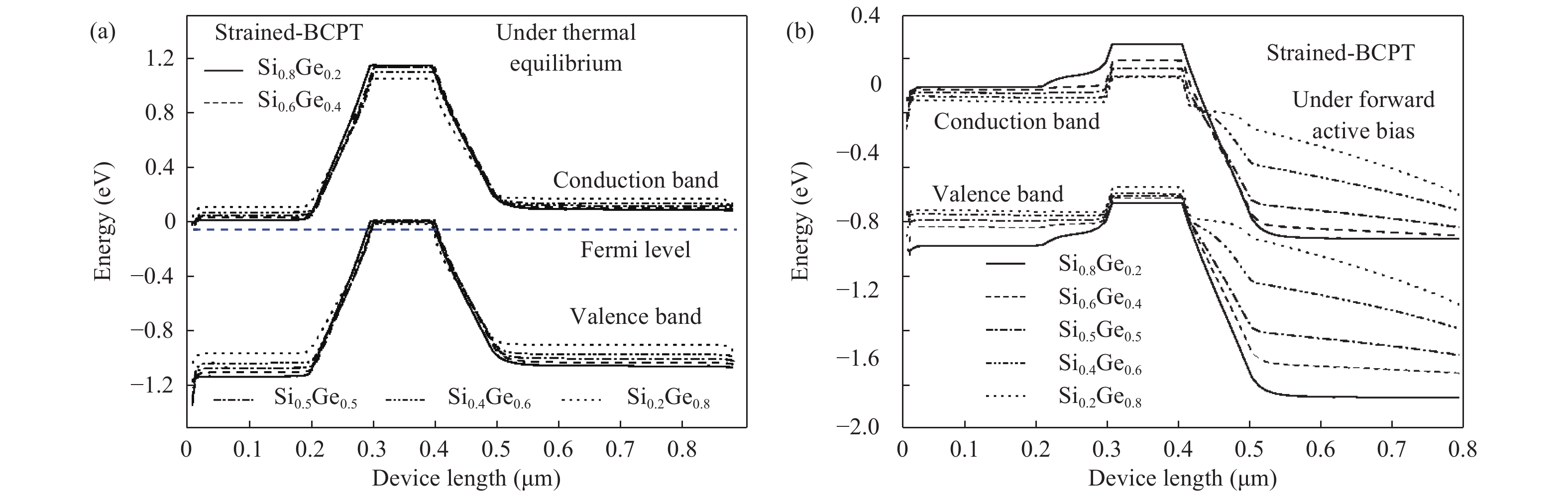
Table 1. Simulation parameters of the conventional BCPT and proposed strained BCPT.
| Parameter | BCPT[11] | Strained BCPT |
| Device layer material | Si | SixGe1−x |
| Semiconductor film thickness (nm) | 15 | 15 |
| Buried oxide thickness (nm) | 375 | 375 |
| Top oxide thickness (nm) | 5 | 5 |
| Background doping (cm−3) | 1013 | 1013 |
| Doping | Undoped | Undoped |
| Emitter length (nm) | 200 | 200 |
| Base length (nm) | 100 | 100 |
| Collector length (nm) | 400 | 400 |
| Isolation between electrodes (nm) | 100 | 100 |
| Emitter electrode (eV) | 3.9 | 3.9 |
| Base electrode (eV) | 5.65 | 5.65 |
| Collector electrode (eV) | 4.28 | 4.28 |
 DownLoad: CSV
| [1] |
Rein H M, Moller M. Design considerations for very-high-speed Si-bipolar IC's operating up to 50 Gb/s. IEEE J Solid-State Circuits, 1996, 31(8): 1076 doi: 10.1109/4.508255
|
| [2] |
Harame D L, Ahlgren D C, Coolbaugh D D, et al. Current status and future trends of SiGe BiCMOS technology. IEEE Trans Electron Devices, 2001, 48(11): 2575 doi: 10.1109/16.960385
|
| [3] |
Voegeli B T, Gray P B, Rainey B A, et al. High performance, low complexity vertical PNP BJT integrated in a 0.18 μm SiGe BiCMOS technology. Proceedings of the Bipolar/BiCMOS Circuits and Technology Meeting, 2005: 136
|
| [4] |
Martinez A, Barker J R, Svizhenko A, et al. The impact of random dopant aggregation in source and drain on the performance of ballistic DG nano-MOSFETs: a NEGF study. IEEE Trans Nanotechnol, 2007, 6(4): 438 doi: 10.1109/TNANO.2007.899638
|
| [5] |
Chiang M H, Lin J N, Kim K, et al. Random dopant fluctuation in limited-width FinFET technologies. IEEE Trans Electron Devices, 2007, 54(8): 2055 doi: 10.1109/TED.2007.901154
|
| [6] |
Singh S, Kondekar P N. Dopingless super-steep impact ionisation MOS (dopingless-IMOS) based on work-function engineering. IET Electron Lett, 2014, 50(12): 888 doi: 10.1049/el.2014.1072
|
| [7] |
Singh S, Pal P, Kondekar P N. Charge-plasma-based super-steep negative capacitance junctionless tunnel field effect transistor: design and performance. Electron Lett, 2014, 50(25): 1963 doi: 10.1049/el.2014.3256
|
| [8] |
Singh S, Kondekar P N. A novel dynamically configurable electrostatically doped silicon nanowire impact ionization MOS. Superlattices Microstruct, 2015, 88: 695 doi: 10.1016/j.spmi.2015.10.033
|
| [9] |
Singh S, Sinha R, Kondekar P N. A novel ultra steep dynamically reconfigurable electrostatically doped silicon nanowire Schottky barrier FET. Superlattices Microstruct, 2016, 93: 40 doi: 10.1016/j.spmi.2016.02.039
|
| [10] |
Rajasekharan B, Hueting R J, Salm C, et al. Fabrication and characterization of the charge-plasma diode. IEEE Electron Device Lett, 2010, 31(6): 528 doi: 10.1109/LED.2010.2045731
|
| [11] |
Kumar M J, Nadda K. Bipolar charge-plasma transistor: a novel three terminal device. IEEE Trans Electron Devices, 2012, 59(4): 962 doi: 10.1109/TED.2012.2184763
|
| [12] |
Nadda K, Kumar M J. Schottky collector bipolar transistor without impurity doped emitter and base: design and performance. IEEE Trans Electron Devices, 2013, 60(9): 2956 doi: 10.1109/TED.2013.2272943
|
| [13] |
Nadda K, Kumar M J. Thin-film bipolar transistors on recrystallized polycrystalline silicon without impurity doped junctions: proposal and investigation. J Display Technol, 2014, 10(7): 590 doi: 10.1109/JDT.2014.2310124
|
| [14] |
Nadda K, Kumar M J. Vertical bipolar charge plasma transistor with buried metal layer. Sci Rep, 2015, 5: 7860 doi: 10.1038/srep07860
|
| [15] |
Persson S, Fjer M, Cousin E E, Olsen S H, et al. Strained-silicon heterojunction bipolar transistor. IEEE Trans Electron Devices, 2010, 57(6): 1243 doi: 10.1109/TED.2010.2045667
|
| [16] |
Lu T C, Kuo J B. A closed-form analytical BJT forward transit time model considering bandgap-narrowing effects and concentration-dependent diffusion coefficients. Solid-State Electron, 1992, 35(9): 1374 doi: 10.1016/0038-1101(92)90175-C
|
| [17] |
Behera P, Mohapatra S K. A comparative study on SiGe HBTs and Si BJTs in nanoscale. Int J Adv Sci Technol, 2014, 71: 59 doi: 10.14257/ijast
|
| [18] |
Clifford K, Hoyt J L, Gibbons J F. Bandgap and transport properties of Si1−xGex by analysis of nearly ideal Si/Si1−xGex/Si heterojunction bipolar transistors. IEEE Trans Electron Devices, 1989, 36(10): 2093 doi: 10.1109/16.40925
|
| [19] |
Huang C J, Sun C J, Grotjohn T A, et al. Temperature dependence and post-stress recovery of hot electron degradation effects in bipolar transistors. IEEE Proc Bipolar Circuits and Technology Meeting, 1991: 170
|
| [20] |
Sheng S R, McAlister S P, Storey C, et al. Hot-carrier induced degradation and recovery in polysilicon-emitter bipolar transistors. Solid-State Electron, 2002, 46(10): 1603 doi: 10.1016/S0038-1101(02)00112-0
|
| [21] |
Gurrum S P, Suman S K, Joshi Y K, et al. Thermal issues in next-generation integrated circuits. IEEE Trans Device Mater. Reliab, 2004, 4(4): 709 doi: 10.1109/TDMR.2004.840160
|
| [22] |
Olsson J. Self-heating effects in SOI bipolar transistors. Microelectron Eng, 2001, 56(3): 339
|
| [23] |
Zhang W R, Yang J W, Liu H J, et al. The temperature dependence of DC characteristics and its implication in microwave power Si/SiGe/Si HBTs. 4th IEEE Int Conf on Microwave and Millimeter Wave Technology, 2004: 594
|
| [24] |
Kumar M J, Singh P. A super beta bipolar transistor using SiGe-base surface accumulation layer transistor (SALTran) concept: A simulation study. IEEE Trans Electron Devices, 2006, 53(3): 577 doi: 10.1109/TED.2005.863538
|
| [25] |
Kumar M J, Parihar V. Surface accumulation layer transistor (SALTran): A new bipolar transistor for enhanced current gain and reduced hot-carrier degradation. IEEE Trans Device Mater Reliab, 2004, 4(3): 509 doi: 10.1109/TDMR.2004.829074
|
| [26] |
Prijic Z, Pavlovic Z, Ristic S, Stojadinovic N. Zero-temperature-coefficient (ZTC) biasing of power VDMOS transistors. Electron Lett, 1993, 29(5): 435 doi: 10.1049/el:19930291
|
| [27] |
Sahu P K, Mohapatra S K, Pradhan K P. Zero temperature-coefficient bias point over wide range of temperatures for single- and double-gate UTB-SOI n-MOSFETs with trapped charges. Mater Sci Semicond Process, 2015, 31: 175 doi: 10.1016/j.mssp.2014.11.036
|
| [28] |
Ward R R, Dawson W J, Zhu L, et al. Power diodes for cryogenic operation. IEEE 34th Annual Power Electronics Specialist Conf, 2003, 4: 1891
|
| [29] |
Momose H S, Hiroshi I. Analysis of the temperature dependence of hot-carrier-induced degradation in bipolar transistors for Bi-CMOS. IEEE Trans Electron Devices, 1994, 41(6): 978 doi: 10.1109/16.293311
|
| [30] |
Webster W M. On the variation of junction-transistor current-amplification factor with emitter current. Proc IRE, 1954, 42(6): 914 doi: 10.1109/JRPROC.1954.274751
|
| [31] |
Kirk C T. A theory of transistor cutoff frequency (fT) falloff at high current densities. IRE Trans Electron Devices, 1962, 9(2): 164 doi: 10.1109/T-ED.1962.14965
|
| [32] |
Tsu R, Hernandez J G. Temperature dependence of silicon Raman lines. Appl Phys Lett, 1982, 41(11): 1016 doi: 10.1063/1.93394
|
| [33] |
Hassan M S, Nomani M W. Base-transit-time model considering field dependent mobility for BJTs operating at high-level injection. IEEE Trans Electron Devices, 2006, 53(10): 2532 doi: 10.1109/TED.2006.882269
|
| [34] |
Loan S A, Bashir F, Rafat M, et al. A high performance charge plasma based lateral bipolar transistor on selective buried oxide. Semicond Sci Technol, 2013, 29(1): 015011
|
| [35] |
Zhang Y R, Zhang B, Li Z J, et al. Two-dimensional analysis of the interface state effect on current gain for a 4H-SiC bipolar junction transistor. Chin Phys B, 2010, 19(6): 067102 doi: 10.1088/1674-1056/19/6/067102
|


Article views: 3808 Times PDF downloads: 24 Times Cited by: 0 Times
Received: 06 July 2018 Revised: 26 September 2018 Online: Accepted Manuscript: 06 November 2018Uncorrected proof: 12 November 2018Published: 13 December 2018
| Citation: |
Sangeeta Singh. Impact of strained silicon on the device performance of a bipolar charge plasma transistor[J]. Journal of Semiconductors, 2018, 39(12): 124011. doi: 10.1088/1674-4926/39/12/124011
****
S Singh, Impact of strained silicon on the device performance of a bipolar charge plasma transistor[J]. J. Semicond., 2018, 39(12): 124011. doi: 10.1088/1674-4926/39/12/124011.

|
| [1] |
Rein H M, Moller M. Design considerations for very-high-speed Si-bipolar IC's operating up to 50 Gb/s. IEEE J Solid-State Circuits, 1996, 31(8): 1076 doi: 10.1109/4.508255
|
| [2] |
Harame D L, Ahlgren D C, Coolbaugh D D, et al. Current status and future trends of SiGe BiCMOS technology. IEEE Trans Electron Devices, 2001, 48(11): 2575 doi: 10.1109/16.960385
|
| [3] |
Voegeli B T, Gray P B, Rainey B A, et al. High performance, low complexity vertical PNP BJT integrated in a 0.18 μm SiGe BiCMOS technology. Proceedings of the Bipolar/BiCMOS Circuits and Technology Meeting, 2005: 136
|
| [4] |
Martinez A, Barker J R, Svizhenko A, et al. The impact of random dopant aggregation in source and drain on the performance of ballistic DG nano-MOSFETs: a NEGF study. IEEE Trans Nanotechnol, 2007, 6(4): 438 doi: 10.1109/TNANO.2007.899638
|
| [5] |
Chiang M H, Lin J N, Kim K, et al. Random dopant fluctuation in limited-width FinFET technologies. IEEE Trans Electron Devices, 2007, 54(8): 2055 doi: 10.1109/TED.2007.901154
|
| [6] |
Singh S, Kondekar P N. Dopingless super-steep impact ionisation MOS (dopingless-IMOS) based on work-function engineering. IET Electron Lett, 2014, 50(12): 888 doi: 10.1049/el.2014.1072
|
| [7] |
Singh S, Pal P, Kondekar P N. Charge-plasma-based super-steep negative capacitance junctionless tunnel field effect transistor: design and performance. Electron Lett, 2014, 50(25): 1963 doi: 10.1049/el.2014.3256
|
| [8] |
Singh S, Kondekar P N. A novel dynamically configurable electrostatically doped silicon nanowire impact ionization MOS. Superlattices Microstruct, 2015, 88: 695 doi: 10.1016/j.spmi.2015.10.033
|
| [9] |
Singh S, Sinha R, Kondekar P N. A novel ultra steep dynamically reconfigurable electrostatically doped silicon nanowire Schottky barrier FET. Superlattices Microstruct, 2016, 93: 40 doi: 10.1016/j.spmi.2016.02.039
|
| [10] |
Rajasekharan B, Hueting R J, Salm C, et al. Fabrication and characterization of the charge-plasma diode. IEEE Electron Device Lett, 2010, 31(6): 528 doi: 10.1109/LED.2010.2045731
|
| [11] |
Kumar M J, Nadda K. Bipolar charge-plasma transistor: a novel three terminal device. IEEE Trans Electron Devices, 2012, 59(4): 962 doi: 10.1109/TED.2012.2184763
|
| [12] |
Nadda K, Kumar M J. Schottky collector bipolar transistor without impurity doped emitter and base: design and performance. IEEE Trans Electron Devices, 2013, 60(9): 2956 doi: 10.1109/TED.2013.2272943
|
| [13] |
Nadda K, Kumar M J. Thin-film bipolar transistors on recrystallized polycrystalline silicon without impurity doped junctions: proposal and investigation. J Display Technol, 2014, 10(7): 590 doi: 10.1109/JDT.2014.2310124
|
| [14] |
Nadda K, Kumar M J. Vertical bipolar charge plasma transistor with buried metal layer. Sci Rep, 2015, 5: 7860 doi: 10.1038/srep07860
|
| [15] |
Persson S, Fjer M, Cousin E E, Olsen S H, et al. Strained-silicon heterojunction bipolar transistor. IEEE Trans Electron Devices, 2010, 57(6): 1243 doi: 10.1109/TED.2010.2045667
|
| [16] |
Lu T C, Kuo J B. A closed-form analytical BJT forward transit time model considering bandgap-narrowing effects and concentration-dependent diffusion coefficients. Solid-State Electron, 1992, 35(9): 1374 doi: 10.1016/0038-1101(92)90175-C
|
| [17] |
Behera P, Mohapatra S K. A comparative study on SiGe HBTs and Si BJTs in nanoscale. Int J Adv Sci Technol, 2014, 71: 59 doi: 10.14257/ijast
|
| [18] |
Clifford K, Hoyt J L, Gibbons J F. Bandgap and transport properties of Si1−xGex by analysis of nearly ideal Si/Si1−xGex/Si heterojunction bipolar transistors. IEEE Trans Electron Devices, 1989, 36(10): 2093 doi: 10.1109/16.40925
|
| [19] |
Huang C J, Sun C J, Grotjohn T A, et al. Temperature dependence and post-stress recovery of hot electron degradation effects in bipolar transistors. IEEE Proc Bipolar Circuits and Technology Meeting, 1991: 170
|
| [20] |
Sheng S R, McAlister S P, Storey C, et al. Hot-carrier induced degradation and recovery in polysilicon-emitter bipolar transistors. Solid-State Electron, 2002, 46(10): 1603 doi: 10.1016/S0038-1101(02)00112-0
|
| [21] |
Gurrum S P, Suman S K, Joshi Y K, et al. Thermal issues in next-generation integrated circuits. IEEE Trans Device Mater. Reliab, 2004, 4(4): 709 doi: 10.1109/TDMR.2004.840160
|
| [22] |
Olsson J. Self-heating effects in SOI bipolar transistors. Microelectron Eng, 2001, 56(3): 339
|
| [23] |
Zhang W R, Yang J W, Liu H J, et al. The temperature dependence of DC characteristics and its implication in microwave power Si/SiGe/Si HBTs. 4th IEEE Int Conf on Microwave and Millimeter Wave Technology, 2004: 594
|
| [24] |
Kumar M J, Singh P. A super beta bipolar transistor using SiGe-base surface accumulation layer transistor (SALTran) concept: A simulation study. IEEE Trans Electron Devices, 2006, 53(3): 577 doi: 10.1109/TED.2005.863538
|
| [25] |
Kumar M J, Parihar V. Surface accumulation layer transistor (SALTran): A new bipolar transistor for enhanced current gain and reduced hot-carrier degradation. IEEE Trans Device Mater Reliab, 2004, 4(3): 509 doi: 10.1109/TDMR.2004.829074
|
| [26] |
Prijic Z, Pavlovic Z, Ristic S, Stojadinovic N. Zero-temperature-coefficient (ZTC) biasing of power VDMOS transistors. Electron Lett, 1993, 29(5): 435 doi: 10.1049/el:19930291
|
| [27] |
Sahu P K, Mohapatra S K, Pradhan K P. Zero temperature-coefficient bias point over wide range of temperatures for single- and double-gate UTB-SOI n-MOSFETs with trapped charges. Mater Sci Semicond Process, 2015, 31: 175 doi: 10.1016/j.mssp.2014.11.036
|
| [28] |
Ward R R, Dawson W J, Zhu L, et al. Power diodes for cryogenic operation. IEEE 34th Annual Power Electronics Specialist Conf, 2003, 4: 1891
|
| [29] |
Momose H S, Hiroshi I. Analysis of the temperature dependence of hot-carrier-induced degradation in bipolar transistors for Bi-CMOS. IEEE Trans Electron Devices, 1994, 41(6): 978 doi: 10.1109/16.293311
|
| [30] |
Webster W M. On the variation of junction-transistor current-amplification factor with emitter current. Proc IRE, 1954, 42(6): 914 doi: 10.1109/JRPROC.1954.274751
|
| [31] |
Kirk C T. A theory of transistor cutoff frequency (fT) falloff at high current densities. IRE Trans Electron Devices, 1962, 9(2): 164 doi: 10.1109/T-ED.1962.14965
|
| [32] |
Tsu R, Hernandez J G. Temperature dependence of silicon Raman lines. Appl Phys Lett, 1982, 41(11): 1016 doi: 10.1063/1.93394
|
| [33] |
Hassan M S, Nomani M W. Base-transit-time model considering field dependent mobility for BJTs operating at high-level injection. IEEE Trans Electron Devices, 2006, 53(10): 2532 doi: 10.1109/TED.2006.882269
|
| [34] |
Loan S A, Bashir F, Rafat M, et al. A high performance charge plasma based lateral bipolar transistor on selective buried oxide. Semicond Sci Technol, 2013, 29(1): 015011
|
| [35] |
Zhang Y R, Zhang B, Li Z J, et al. Two-dimensional analysis of the interface state effect on current gain for a 4H-SiC bipolar junction transistor. Chin Phys B, 2010, 19(6): 067102 doi: 10.1088/1674-1056/19/6/067102
|

 WeChat ID
Journal of Semiconductors © 2017 All Rights Reserved 京ICP备05085259号-2