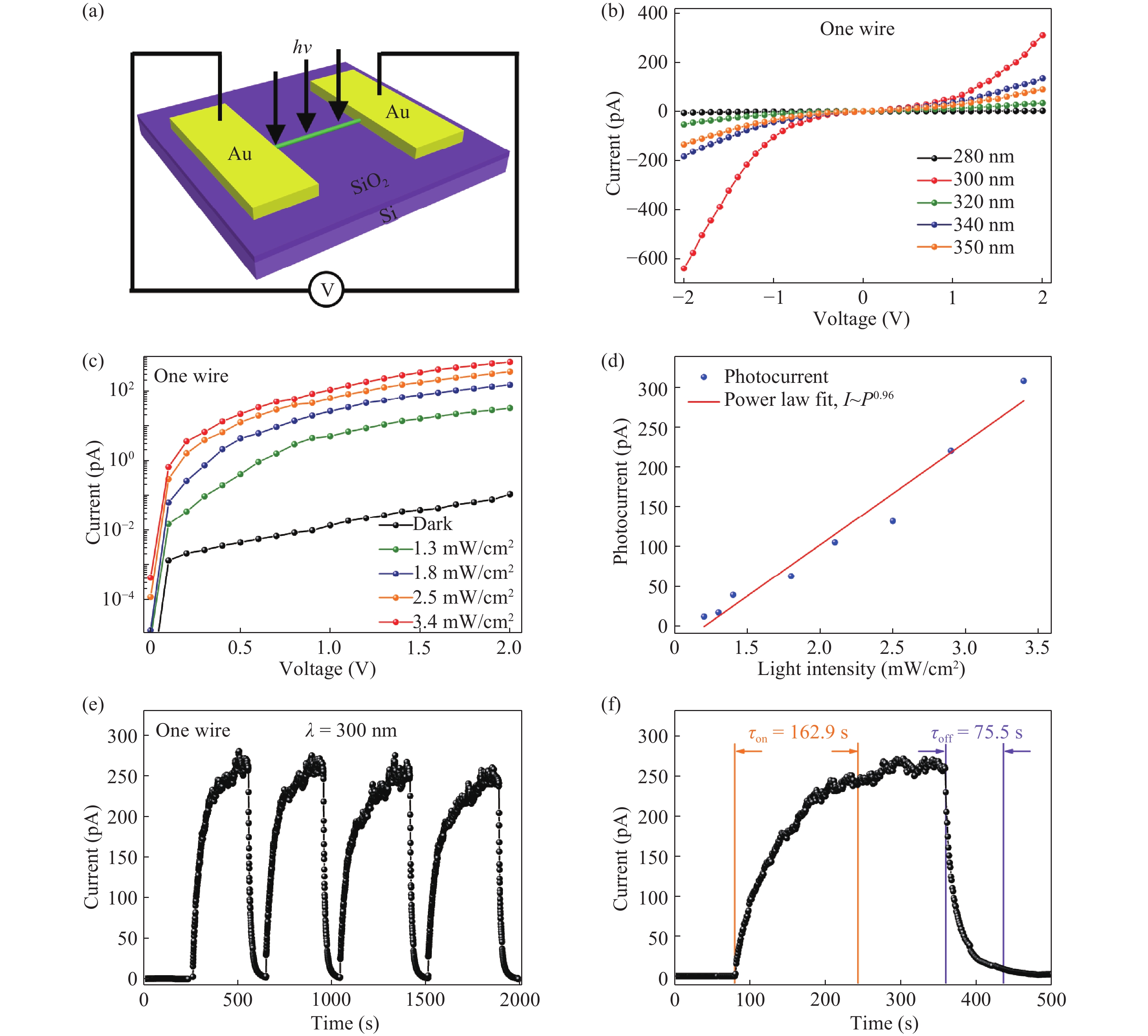
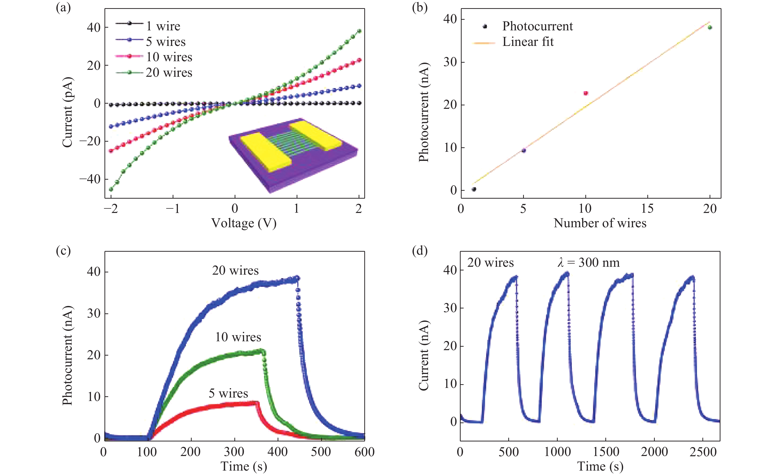
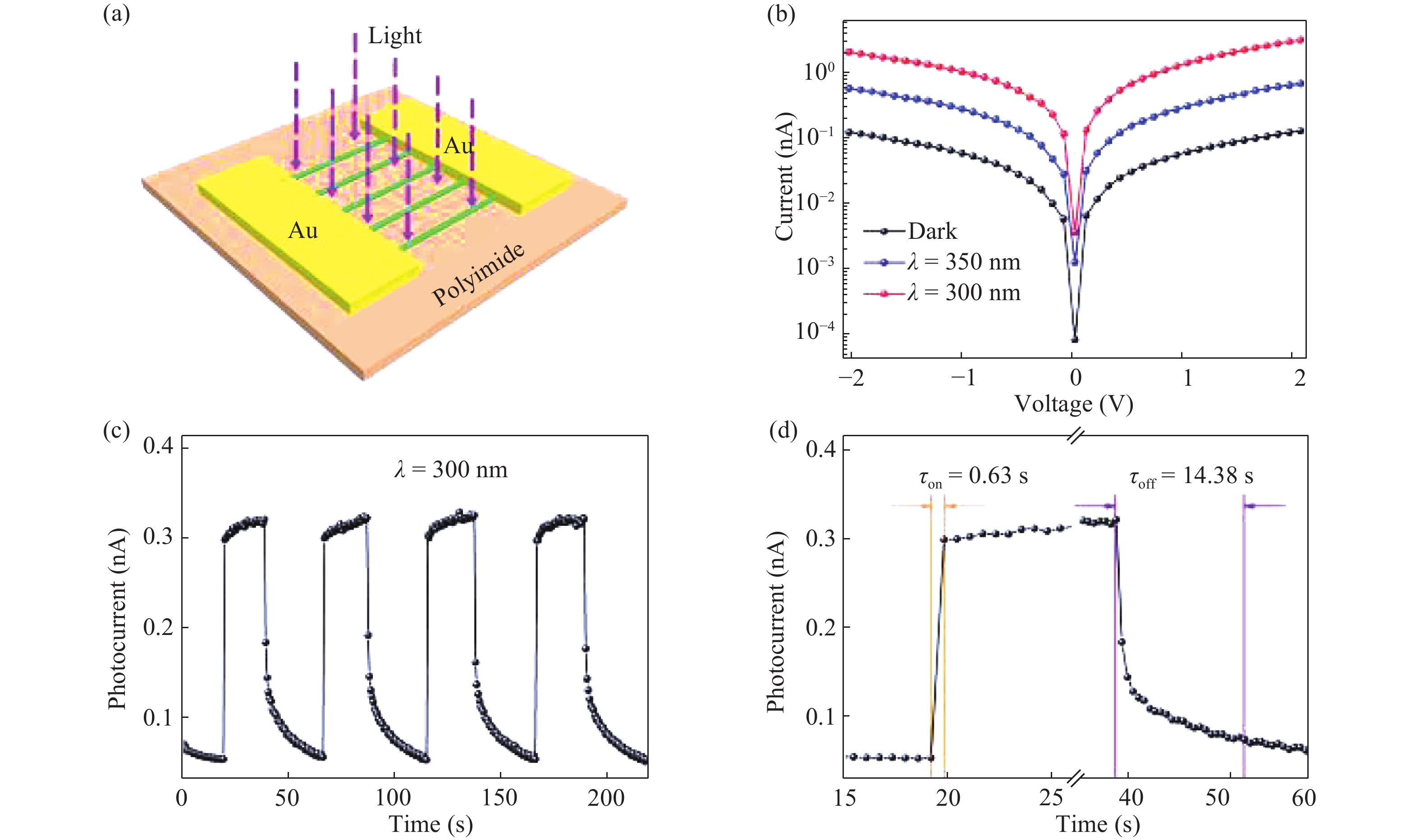
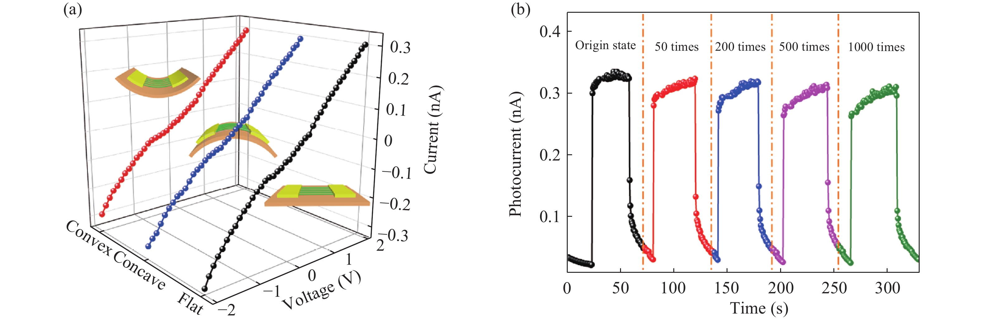
J. Semicond. > 2018, Volume 39 > Issue 2 > 024002

SEMICONDUCTOR DEVICES

Flexible ultraviolet photodetectors based on ZnO–SnO2 heterojunction nanowire arrays

Zheng Lou1, 2, Xiaoli Yang1, Haoran Chen2 and Zhongzhu Liang3,

+ Author Affiliations

 Corresponding author: Zhongzhu Liang, liangzz@ciomp.ac.cn

DOI: 10.1088/1674-4926/39/2/024002

PDF

Turn off MathJax

Abstract: A ZnO–SnO2 nanowires (NWs) array, as a metal oxide semiconductor, was successfully synthesized by a near-field electrospinning method for the applications as high performance ultraviolet photodetectors. Ultraviolet photodetectors based on a single nanowire exhibited excellent photoresponse properties to 300 nm ultraviolet light illumination including ultrahigh Ion/Ioff ratios (up to 103), good stability and reproducibility because of the separation between photo-generated electron-hole pairs. Moreover, the NWs array shows an enhanced photosensing performance. Flexible photodetectors on the PI substrates with similar tendency properties were also fabricated. In addition, under various bending curvatures and cycles, the as-fabricated flexible photodetectors revealed mechanical flexibility and good stable electrical properties, showing that they have the potential for applications in future flexible photoelectron devices.

Key words: nanowirephotodetectorheterojunction

Ultraviolet (UV) photodetectors have attracted extensive attention due to their broad applications in biological and environmental fields, missile-launch detection and digital imaging, and optical communications[13]. The 1D nanostructure is capable of providing a big aspect ratio, direct transmitting channel for the charge transfer process[410]. By dint of this special geometrical and electrical efficiency, nanowires (NWs) are extensively utilized in UV photodetection. Considerable efforts have been devoted to fabricate NWs based UV photodetectors using semiconductors with a wide bandgap, such as ZnO, TiO2, SnO2, and ternary metal oxides[1114]. 1D materials with heterostructures have properties not merely from each component, but also the occurrence of a reaction on the interface of each component while in comparison with pure semiconducting material[1518]. Particularly, the 1D heterosturestures NWs based photodetector showed a much better photoresponse than that of the individual ones, as the photogenerated carriers can be spatially separated at the interface. For example, Tian et al. have made the new ZnS-ZnO branched nanostructures based photodetector that exhibits excellent performances compared with those of pure ZnS nanowires[19]. Chong and his co-workers designed a TiO2–ZnTiO3 heterojunction nanowire-based photodetector with increasing the device’s photosensitivity, spectra responsivity and external quantum efficiency[20]. Therefore, the construction of 1D heterostructures provided a significant pathway and new views to acquire optoelectronics devices with super performance.

In recent years, assembling the NWs array as great construction blocks can achieve the request of miniaturization and multiple functions for the photoelectric instruments[21]. Even though lots of strategies have been proposed, assembling perfectly arrayed NWs in an effective and inexpensive way remains a challenge[22]. The near-field electrospinning NWs array has been utilized in tissue engineering, solar batteries, sensing elements, transistors, and so on[23, 24]. The advantages of this new processing for manufacturing the 1D nano-structures are low cost, efficiency, and convenience to be assemblied into nanofilms[25]. ZnO and SnO2, as significant semiconducting material with wide band-gaps of 3.37 and 3.6 eV, have been researched in an intensive manner as the useful parts in the visible-blind UV photodetectors, on account of the high-performance of the photoelectronic property[11, 26]. The ZnO–SnO2 heterostructure NWs array may have the advantages for the UV photodetector, such as high stability, large Ion/Ioff ratio, and relatively fast response speed.

Hererin, we report the successful fabrication of UV photodetectors with 1D ZnO–SnO2 heterostructure array, obtained from the near-field electrospinning method. The as-fabricated photodetectors showed high Ion/Ioff ratio up to 103 with high response to ultraviolet incident light. All the parameters are determined by the numbers of the NWs. Besides, flexible photodetectors are also fabricated for the first time. Due to the robust flexibility and excellent stability, there is a strong possibility of them being used as the future flexible electronics.

Firstly, Zn(NO3)2·6H2O (Aladdin, 99.9%) and SnCl4 (Aladdin, 99.9%) with a molar ratio of 1 : 1 are dissolved in a mixed solution that consisted of ethanol (99.7%) and dimethylformamide (DMF, 99.9%) with a volume ratio of 1 : 1. The mixed solution is processed under magnetic stirring until a uniform solution is obtained. Subsequently, polyvinylpyrrolidone (PVP, molecular weight of 1300000, Sigma-aldrich) with a concentration of 12 wt% in DMF solution is added in the above solution. Under powerful magnetic stirring for 4 h, a transparent and homogeneous solution is obtained. Then, 1 mL of the solution is sucked into the injection syringe to prepare for electrospinning.

We choose two different substrates (SiO2 and Polyimide) as the collectors in order to study their various optoelectronic properties. The electrospinning parameters are different for different collectors. Here, the collectors should be grounded. A high voltage (+1.60 kV for SiO2 and +1.50 kV for polyimide) is applied to the stainless steel needle of the syringe and the top of the needle is controlled with a distance of 5 mm to the collector. When the Taylor Cone appears and it begins to spin, turn on the x-y moving stage to control the moving trajectory with a moving speed of 10 cm/s. In this way, aligned ZnO–SnO2 NWs arrays can be prepared on different substrates. The distance (> 5μm commonly) between two neighboring NWs can be adjusted by setting different y-axis values. To remove organic compositions and promote crystallization of grain, the NWs arrays on different substrates are calcined (at 550 °C for SiO2 and 400 °C for polyimide) for 2 h at air atmosphere. Then, the samples are cooled down to room temperature naturally and the ZnO–SnO2 NWs arrays are obtained.

To investigate the optoelectronic properties of ZnO–SnO2 nanowires, the photodetectors are fabricated by a traditional photolithography process. 50 nm Au electrodes are evaporated thermally on both sides of as-prepared ZnO/SnO2 arrays. The photodetectors based on single wire and multi-wires on flexible and rigid substrates are fabricated by this method. A semiconductor parameter analyzer (Keithley 4200-SCS) with probe station is used to test the optoelectronic properties of ZnO–SnO2 devices. Ultraviolet light is emitted by a power adjustable light source system (CEL-HXF300) and an Ophir NOVA power meter is used to test the incident ultraviolet light intensity. All tests are finished at room temperature and in air atmosphere.

The size and morphology of the electrospun ZnO–SnO2 nanowires are observed by optical microscope (BX51, OLYMPUS) and scanning electron microscope (Zeiss, Supra55 (VP)). The composition of the products is analyzed by a powder X-ray diffractometer (XRD, Rigaku D/Max-2550, λ = 1.5418 Å). The flexible performance of the photodetector on polyimide substrate is tested by a one-dimensional moving stage, which can fix both ends of the devices.

The photodetectors based on ZnO–SnO2 hybrid NWs array were built by a modified near-field electro-spinning method. Due to the high voltage between the vessel outlet and the collector, two separate electrodes on the collector make the NWs assemble orderly (2a). Before electrospinning, the precursors were mixed with a polyvinyl pyrrolidone (PVP) solution, which was dissolved in dimethyl formamide (DMF). They were then annealed in air after the NWs array formed to remove excess PVP. The optical and SEM images of ZnO– SnO2 hybrid NWs are illustrated, respectively in Figs. 1(b)1(d). All NWs were assembled abreast forming a thin uniform layer. The density of the array could be adjusted by changing the electrospinning parameter, including the electrospinning time and the rate of precursor feeding. XRD was used to identify the compositions of the hybrid NWs (Fig. 2(e)). The XRD test result of the as-prepared 1D ZnO–SnO2 heterostructure, revealed peaks from only SnO2 (JCPDS No. 77-0447) and ZnO (JCPDS No. 36-1451) phases.

Figure  1.  (Color online) (a) Setup of the electrospinning machine. (b) Optical images of the as-synthesized ZnO–SnO2 heterostructure NWs array. (c, d) SEM image of ZnO–SnO2 heterostructure NWs array. (e) XRD pattern of the as-synthesized products.

As depicted in the Experimental Section, photodetectors were then built on individual 1D ZnO–SnO2 heterostructures according to the standard procedures. The schematic illustration in Fig. 2(a) is a single ZnO–SnO2 NW photodetector under illumination for measuring the photoresponsivity. Shown in Fig. 2(b) is the graph of current against voltage of the device in the dark and under light with different wavelengths. When the device was put under illumination, the photocurrent significantly increased. The dark current was approximately 200 fA, and the photocurrent could reach 300 pA when the device was exposed to light with a wavelength of 300 nm, exhibiting an ultrahigh Ion/Ioff ratio ~1.5 × 10³. Furthermore, the device has also shown a great photoresponsivity under ultraviolet light with different wavelengths (280 to 350 nm). Fig. 2(c) illustrates the test result of the relationship between current and voltage of the photodetector in the dark and exposed to different intensities (1.3 to 3.4 mW/cm2) of 300 nm light irradiation. We can see that at the same voltage, the light current increases sharply with the increasing light intensities, because the absorbed photon flux adjusts the efficiency of photogenerated charge carrier. The relationship between photocurrent and light intensity is shown by a power law (Fig. 2(e)), I = APθ, which can be interpreted as follows: the photocurrent I, a constant A, the light intensity P and the empirical value θ. As shown in Fig. 2(d), the photocurrent is strongly correlated with light intensity. The value of θ is 0.96 (I~P0.96) with a voltage within 2 V, which demonstrates that the ZnO–SnO2 NWs possess an amazing photocurrent capability and linearity. Another important parameter of the photodetector is the time-dependent photoresponsivity. Fig. 2(e) illustrates that measurements were taken in four cycles at a voltage of 2 V with the testing condition switching between total darkness and illumination of 3.4 mW/cm2 UV light. It was also found that the photocurrent is not affected by switching on/off the illumination during the four cycles, showing that the photodetector has great stability and reproducibility. Fig. 2(f) illustrates one cycle from Fig. 2(e). The rise and decay time was defined as the time interval for the peak value of the photocurrent to change between 10% and 90%. Its values were about 162.5 and 75.5 s, respectively.

Figure  2.  (Color online) (a) Schematic illustration of as-fabricated photodetector. (b) IV curves of the photodetector under various wavelength lights and in the dark. (c) IV test result of the device under different power intensities of 300 nm light illumination and in the dark. (d) The dependence of photocurrent on light intensity. (e) Photoresponse characteristics of the device. (f) Enlarged view of (e).

Following are some explanations of the high photoresponsivity of the ZnO–SnO2 heterostructures. Firstly, a thicker charge depletion layer was formed because more oxygen molecules were absorbed by the 1D heterostructures with large surface area. This results in lower dark current. Secondly, the existence of the ZnO–SnO2 interface, which results in a junction barrier, further decreased the dark current. Moreover, the energy band alignment of the 1D ZnO–SnO2 heterostructure is also responsible for the performance improvement. Under light illumination, electron-hole pairs were generated and electrons were transferred to SnO2, forming a charge transfer state, which led to a spatial distribution of the charge carriers. The carrier density increases sharply and the barrier height decreases due to the separation of the photogenerated electron-hole pair. As a result, there was a decrease in the recombination rate of the carriers.

A hybrid NWs based photodetector can further enhance the photo sensing performance by increasing the number of the NWs of the array. Fig. 3(a) shows the IV curves of different numbers of NWs. As illustrated, the photocurrents of the photodetector increased as the NWs increased, from 308 pA to 9.3 nA, 22.8, nA and 38.1 nA. The inset of Fig. 3(a) is a schematic diagram of the nanowire array photodetectors. The fitted curve shown in Fig. 3(b) reveals the good linearity of the photocurrent with the number of NWs changing. This result shows that we can provide different performances of the photodetector according to the needs of different application scenarios. Fig. 3(c) shows the single response and recovery curve of the 5, 10, and 20 NWs based photodetectors, respectively. As can be seen, the response and recovery time did not change with increasing the NWs. However, the photoresponse of the 20 NWs device had an obvious improvement. Fig. 3(d) illustrates the measurement of the photoresponsivity of the 20 NWs based photodetector by repeatedly turning on/off the 300 nm light. During the four given cycles, no significant change in photocurrent was observed, which indicates that the device has great stability and reproducibility.

Figure  3.  (Color online) (a) IV curves of the photodetector based on different numbers of NWs. (b) The dependence of photocurrent on the number of NWs. (d) Single photoresponse curve of 5, 10, 20 NWs. (d) Photoresponse characteristics of 20 NWs device.

Recently, portable and flexible electronics have greatly developed, resulting in that flexible sensors and detectors are urgently needed. To study the potential applications of ZnO–SnO2 NW in flexible electronics, ZnO–SnO2 NW based photodetectors were built on flexible PI substrate, as shown in Fig. 4(a), which is the schematic illustration of the ZnO–SnO2 NW array flexible photodetector. As shown in Fig. 4(b), the relationship between photocurrent and voltage of the flexible photodetector is investigated under the 300 and 350 nm light illumination and in dark conditions. It is observed that the flexible device was also highly sensitive to UV light with an excellent photoresponsivity. Meanwhile, the photocurrent significantly increases under 300 nm incident light at the identical voltage. As shown in Fig. 4(c), the recovery and response properties of the flexible device were also investigated. No significant change in photocurrent was observed, indicating that through the cyclic test the as-fabricated flexible photodetectors have high reproducibility. Moreover, as illustrated in Fig. 4(d), the values of the rise and decay time were 0.63 and 14.38 s, respectively. These behaviors are consistent with those of rigid SiO2/Si substrates. In addition, the reason the photoresponse of the device is a little decreased is the poorer contact between NWs and the flexible substrate. In the flexible device, the polymer PI was used as the flexible substrate. The contact between NW and PI substrate is poorer than that of NW and SiO2/Si substrate. This will degrade the device performance and result in a relatively low light current for photodetectors based on a flexible substrate compared to photodetectors based on SiO2/Si substrate.

Figure  4.  (Color online) (a) Schematic illustration of as-fabricated flexible photodetector. (b) IV curves of the flexible device under 300 and 350 nm light and in the dark. (c) Photoresponse characteristics of the device. (d) Enlarged view of (c).

The electrical stability is a key factor for the measurement of a flexible electrical device. Therefore, as shown in Fig. 5(a), we measured the photoresponse of the device under various curvatures. The different bending curvatures of the detector can be achieved by setting the two stages at different horizontal distances, which resulted in three different bending testing states that are marked as convex, concave and flat (insets in Fig. 5(a)), respectively. The IV curves were measured at each state. No significant change in the curves was observed, indicating that the conductance of the device is not affected by bending stress. The observation concludes that the flexible device has great mechanical flexibility and electrical stability. Furthermore, measurements of the device were taken at a voltage of 2 V at different bending times for 50, 200, 500, and 1000 cycles, by switching between 300 nm UV light and total darkness. The flexible photodetector shows high photoresponsivity to UV light. Moreover, no significant change in the conductance of the flexible device was observed, showing that the flexible ZnO–SnO2 device has an outstanding folding tolerance. The measurements above have shown that 1D ZnO–SnO2 heterostructure based flexible photodetectors have an excellent flexibility, which means that they have the potential to be applied in future flexible and portable devices.

Figure  5.  (Color online) (a) The IV characteristics of the flexible photodetector under different bending conditions. (b) Photoresponse characteristics of the flexible photodetector under different bending cycles.

In summary, we fabricated high performance UV photodetectors using 1D ZnO–SnO2 heterostructures NW array as the sensing materials. As-fabricated devices exhibited a great photoresponse on the UV light (28–50 nm), which showed a good sensitivity to UV light. Flexible photodetectors were also fabricated on PI substate. Studies found that both of the two devices showed excellent properties such as highIon/Ioff and good reversibility, which may be due to the spatial separation of the photogenerated carriers at the interface within the NWs. In addition, the flexible devices exhibited good stable mechanical ability, even after a 1000-cycle bending test, the current still maintains the original value. Our results indicate that the presently constructed ZnO–SnO2 photodetectors in the UV spectrum with ultrahigh sensitivity, fast response speed and good flexibility have a great potential as photoelectronic switches, optoelectronic circuits and so on.


[1]
Sang L W, Liao M Y, Sumiya M. A comprehensive review of semiconductor ultraviolet photodetectors: from thin film to one-dimensional nanostructures. Sensors, 2013, 13: 0482
[2]
Omnes F, Monroy E, Munoz E, et al. Wide bandgap UV photodetectors: a short review of devices and applications. Proc SPIE, 2007, 6473: 64730E
[3]
Alaie Z, Nejad S M, Yousefi M H. Recent advances in ultraviolet photodetectors. Mater Sci Semicond Process, 2015, 29: 16 doi: 10.1016/j.mssp.2014.02.054
[4]
Xiang J, Lu W, Hu Y J, et al. Ge/Si nanowire heterostructures as high-performance field-effect transistors. Nature, 2006, 441: 489 doi: 10.1038/nature04796
[5]
Hwang Y J, Boukai A, Yang P D. High density n-Si/n-TiO2 core/shell nanowire arrays with enhanced photoactivity. Nano Lett, 2009, 9: 410 doi: 10.1021/nl8032763
[6]
Huang X, Wang M, Willinger M G, et al. Assembly of three-dimensional hetero-epitaxial ZnO/ZnS core/shell nanorod and single crystalline hollow ZnS nanotube arrays. ACS Nano, 2012, 6: 7333 doi: 10.1021/nn3024514
[7]
Xu J Y, Ma L, Guo P F, et al. Room-temperature dual-wavelength lasing from single-nanoribbon lateral heterostructures. J Am Chem Soc, 2012, 134: 12394 doi: 10.1021/ja3050458
[8]
Wang X F, Song W F, Liu B, et al. High-performance organic-inorganic hybrid photodetectors based on P3HT:CdSe nanowire heterojunctions on rigid and flexible substrates. Adv Funct Mater, 2013, 23: 1202 doi: 10.1002/adfm.v23.9
[9]
Kalisky B, Spanton E M, Noad H, et al. Locally enhanced conductivity due to the tetragonal domain structure in LaAlO3/SrTiO3 heterointerfaces. Nat Mater, 2013, 12: 1091 doi: 10.1038/nmat3753
[10]
Wang Z R, Wang H, Liu B, et al. Transferable and flexible nanorod-assembled TiO2 cloths for dye-sensitized solar cells, photodetectors, and photocatalysts. ACS Nano, 2011, 5: 8412 doi: 10.1021/nn203315k
[11]
Soci C, Zhang A, Xiang B, et al. ZnO nanowire UV photodetectors with high internal gain. Nano Lett, 2007, 7: 1003 doi: 10.1021/nl070111x
[12]
Tsai T Y, Chang S J, Weng W Y, et al. Synthesis, characterization and electrochemical properties of capsule-like NiO nanoparticles. J Electrochem Soc, 2012, 159: J132 doi: 10.1149/2.008205jes
[13]
Hu L F, Yan J, Liao M Y, et al. Ultrahigh external quantum efficiency from thin SnO2 nanowire ultraviolet photodetectors. Small, 2011, 7: 1012 doi: 10.1002/smll.201002379
[14]
Lou Z, Li L D, Shen G Z. InGaO3(ZnO) superlattice nanowires for high-performance ultraviolet photodetectors. Adv Electron Mater, 2015, 1: 1500054 doi: 10.1002/aelm.201500054
[15]
Lou Z, Shen G Z. Flexible photodetectors based on one-dimensional inorganic nanostructures. Adv Sci, 2016, 1: 1500287
[16]
Wang X F, Liu B, Liu R, et al. Fiber-based flexible all-solid-state asymmetric supercapacitors for integrated photodetecting system. Angew Chem, 2014, 126: 1880 doi: 10.1002/ange.201307581
[17]
Liu Z, Luo T, Liang B, et al. High-detectivity InAs nanowire photodetectors with spectral response from ultraviolet to near-infrared. Nano Res, 2013, 6: 775 doi: 10.1007/s12274-013-0356-0
[18]
Chen G, Liang B, Liu X, et al. High-performance hybrid phenyl-C61-butyric acid methyl ester/Cd3P2 nanowire ultraviolet-visible-near infrared photodetectors. ACS Nano, 2014, 8: 787 doi: 10.1021/nn405442z
[19]
Tian W, Zhang C, Zhai T Y, et al. Flexible ultraviolet photodetectors with broad photoresponse based on branched ZnS–ZnO heterostructure nanofilms. Adv Mater, 2014, 26: 3088 doi: 10.1002/adma.201305457
[20]
Chong H N, Wei G D, Hou H L, et al. High-performance solar-blind ultraviolet photodetector based on electrospun TiO2–ZnTiO3 heterojunction nanowires. Nano Res, 2015, 8: 2822 doi: 10.1007/s12274-015-0787-x
[21]
Liu Z, Xu J, Chen D, et al. Flexible electronics based on inorganic nanowires. Chem Soc Rev, 2015, 44: 161 doi: 10.1039/C4CS00116H
[22]
Zheng Z, Gan L, Zhai T Y. An enhanced UV–Vis–NIR an d flexible photodetector based on electrospun ZnO nanowire array/PbS quantum dots film heterostructure. Adv Sci, 2017, 4: 1600316 doi: 10.1002/advs.201600316
[23]
Greiner A, Wendorff J H. Electrospinning: a fascinating method for the preparation of ultrathin fibers. Angew Chem Int Ed, 2007, 46: 5670 doi: 10.1002/(ISSN)1521-3773
[24]
Wu H, Sun Y, Lin D D, et al. GaN nanofibers based on electrospinning: facile synthesis, controlled assembly, precise doping, and application as high performance UV photodetector. Adv Mater, 2009, 21: 227 doi: 10.1002/adma.v21:2
[25]
Hu L F, Wu L M, Liao M Y, et al. ZnS nanostructure arrays: a developing material star. Adv Mater, 2011, 23: 1988 doi: 10.1002/adma.201004109
[26]
Shi H P, Cheng B C, Cai Q S, et al. Surface state controlled ultrahigh selectivity and sensitivity for UV photodetectors based on individual SnO2 nanowires. J Mater Chem C, 2016, 4: 8399 doi: 10.1039/C6TC02420C
[27]
Lou Z. Li L D, Shen G Z, High-performance rigid and flexible ultraviolet photodetectors with single-crystalline ZnGa2O4. Nano Res, 2015, 8: 2162 doi: 10.1007/s12274-015-0723-0
[28]
Lou Z, Li L D, Shen G Z. Ultraviolet/visible photodetectors with ultrafast, high photosensitivity based on 1D ZnS/CdS heterostructures. Nanoscale, 2016, 8: 5219 doi: 10.1039/C5NR08792A
Fig. 1.  (Color online) (a) Setup of the electrospinning machine. (b) Optical images of the as-synthesized ZnO–SnO2 heterostructure NWs array. (c, d) SEM image of ZnO–SnO2 heterostructure NWs array. (e) XRD pattern of the as-synthesized products.

Fig. 2.  (Color online) (a) Schematic illustration of as-fabricated photodetector. (b) IV curves of the photodetector under various wavelength lights and in the dark. (c) IV test result of the device under different power intensities of 300 nm light illumination and in the dark. (d) The dependence of photocurrent on light intensity. (e) Photoresponse characteristics of the device. (f) Enlarged view of (e).

Fig. 3.  (Color online) (a) IV curves of the photodetector based on different numbers of NWs. (b) The dependence of photocurrent on the number of NWs. (d) Single photoresponse curve of 5, 10, 20 NWs. (d) Photoresponse characteristics of 20 NWs device.

Fig. 4.  (Color online) (a) Schematic illustration of as-fabricated flexible photodetector. (b) IV curves of the flexible device under 300 and 350 nm light and in the dark. (c) Photoresponse characteristics of the device. (d) Enlarged view of (c).

Fig. 5.  (Color online) (a) The IV characteristics of the flexible photodetector under different bending conditions. (b) Photoresponse characteristics of the flexible photodetector under different bending cycles.

[1]
Sang L W, Liao M Y, Sumiya M. A comprehensive review of semiconductor ultraviolet photodetectors: from thin film to one-dimensional nanostructures. Sensors, 2013, 13: 0482
[2]
Omnes F, Monroy E, Munoz E, et al. Wide bandgap UV photodetectors: a short review of devices and applications. Proc SPIE, 2007, 6473: 64730E
[3]
Alaie Z, Nejad S M, Yousefi M H. Recent advances in ultraviolet photodetectors. Mater Sci Semicond Process, 2015, 29: 16 doi: 10.1016/j.mssp.2014.02.054
[4]
Xiang J, Lu W, Hu Y J, et al. Ge/Si nanowire heterostructures as high-performance field-effect transistors. Nature, 2006, 441: 489 doi: 10.1038/nature04796
[5]
Hwang Y J, Boukai A, Yang P D. High density n-Si/n-TiO2 core/shell nanowire arrays with enhanced photoactivity. Nano Lett, 2009, 9: 410 doi: 10.1021/nl8032763
[6]
Huang X, Wang M, Willinger M G, et al. Assembly of three-dimensional hetero-epitaxial ZnO/ZnS core/shell nanorod and single crystalline hollow ZnS nanotube arrays. ACS Nano, 2012, 6: 7333 doi: 10.1021/nn3024514
[7]
Xu J Y, Ma L, Guo P F, et al. Room-temperature dual-wavelength lasing from single-nanoribbon lateral heterostructures. J Am Chem Soc, 2012, 134: 12394 doi: 10.1021/ja3050458
[8]
Wang X F, Song W F, Liu B, et al. High-performance organic-inorganic hybrid photodetectors based on P3HT:CdSe nanowire heterojunctions on rigid and flexible substrates. Adv Funct Mater, 2013, 23: 1202 doi: 10.1002/adfm.v23.9
[9]
Kalisky B, Spanton E M, Noad H, et al. Locally enhanced conductivity due to the tetragonal domain structure in LaAlO3/SrTiO3 heterointerfaces. Nat Mater, 2013, 12: 1091 doi: 10.1038/nmat3753
[10]
Wang Z R, Wang H, Liu B, et al. Transferable and flexible nanorod-assembled TiO2 cloths for dye-sensitized solar cells, photodetectors, and photocatalysts. ACS Nano, 2011, 5: 8412 doi: 10.1021/nn203315k
[11]
Soci C, Zhang A, Xiang B, et al. ZnO nanowire UV photodetectors with high internal gain. Nano Lett, 2007, 7: 1003 doi: 10.1021/nl070111x
[12]
Tsai T Y, Chang S J, Weng W Y, et al. Synthesis, characterization and electrochemical properties of capsule-like NiO nanoparticles. J Electrochem Soc, 2012, 159: J132 doi: 10.1149/2.008205jes
[13]
Hu L F, Yan J, Liao M Y, et al. Ultrahigh external quantum efficiency from thin SnO2 nanowire ultraviolet photodetectors. Small, 2011, 7: 1012 doi: 10.1002/smll.201002379
[14]
Lou Z, Li L D, Shen G Z. InGaO3(ZnO) superlattice nanowires for high-performance ultraviolet photodetectors. Adv Electron Mater, 2015, 1: 1500054 doi: 10.1002/aelm.201500054
[15]
Lou Z, Shen G Z. Flexible photodetectors based on one-dimensional inorganic nanostructures. Adv Sci, 2016, 1: 1500287
[16]
Wang X F, Liu B, Liu R, et al. Fiber-based flexible all-solid-state asymmetric supercapacitors for integrated photodetecting system. Angew Chem, 2014, 126: 1880 doi: 10.1002/ange.201307581
[17]
Liu Z, Luo T, Liang B, et al. High-detectivity InAs nanowire photodetectors with spectral response from ultraviolet to near-infrared. Nano Res, 2013, 6: 775 doi: 10.1007/s12274-013-0356-0
[18]
Chen G, Liang B, Liu X, et al. High-performance hybrid phenyl-C61-butyric acid methyl ester/Cd3P2 nanowire ultraviolet-visible-near infrared photodetectors. ACS Nano, 2014, 8: 787 doi: 10.1021/nn405442z
[19]
Tian W, Zhang C, Zhai T Y, et al. Flexible ultraviolet photodetectors with broad photoresponse based on branched ZnS–ZnO heterostructure nanofilms. Adv Mater, 2014, 26: 3088 doi: 10.1002/adma.201305457
[20]
Chong H N, Wei G D, Hou H L, et al. High-performance solar-blind ultraviolet photodetector based on electrospun TiO2–ZnTiO3 heterojunction nanowires. Nano Res, 2015, 8: 2822 doi: 10.1007/s12274-015-0787-x
[21]
Liu Z, Xu J, Chen D, et al. Flexible electronics based on inorganic nanowires. Chem Soc Rev, 2015, 44: 161 doi: 10.1039/C4CS00116H
[22]
Zheng Z, Gan L, Zhai T Y. An enhanced UV–Vis–NIR an d flexible photodetector based on electrospun ZnO nanowire array/PbS quantum dots film heterostructure. Adv Sci, 2017, 4: 1600316 doi: 10.1002/advs.201600316
[23]
Greiner A, Wendorff J H. Electrospinning: a fascinating method for the preparation of ultrathin fibers. Angew Chem Int Ed, 2007, 46: 5670 doi: 10.1002/(ISSN)1521-3773
[24]
Wu H, Sun Y, Lin D D, et al. GaN nanofibers based on electrospinning: facile synthesis, controlled assembly, precise doping, and application as high performance UV photodetector. Adv Mater, 2009, 21: 227 doi: 10.1002/adma.v21:2
[25]
Hu L F, Wu L M, Liao M Y, et al. ZnS nanostructure arrays: a developing material star. Adv Mater, 2011, 23: 1988 doi: 10.1002/adma.201004109
[26]
Shi H P, Cheng B C, Cai Q S, et al. Surface state controlled ultrahigh selectivity and sensitivity for UV photodetectors based on individual SnO2 nanowires. J Mater Chem C, 2016, 4: 8399 doi: 10.1039/C6TC02420C
[27]
Lou Z. Li L D, Shen G Z, High-performance rigid and flexible ultraviolet photodetectors with single-crystalline ZnGa2O4. Nano Res, 2015, 8: 2162 doi: 10.1007/s12274-015-0723-0
[28]
Lou Z, Li L D, Shen G Z. Ultraviolet/visible photodetectors with ultrafast, high photosensitivity based on 1D ZnS/CdS heterostructures. Nanoscale, 2016, 8: 5219 doi: 10.1039/C5NR08792A
1

Research on heterojunction semiconductor photodetectors based on CsPbBr3 QDs/CsPbBrxI3–x QDs

Chenguang Shen, Mengwei Chen, Wei Huang, Yingping Yang

Journal of Semiconductors. doi: 10.1088/1674-4926/25010022

2

Multi-functional PbI2 enables self-driven perovskite nanowire photodetector with ultra-weak light detection ability

Yapeng Tang, Bo’ao Xiao, Dingjun Wu, Hai Zhou

Journal of Semiconductors, 2025, 46(5): 052801. doi: 10.1088/1674-4926/24110016

3

Photodetector based on Ruddlesden-Popper perovskite microwires with broader band detection

Yongxu Yan, Zhexin Li, Zheng Lou

Journal of Semiconductors, 2023, 44(8): 082201. doi: 10.1088/1674-4926/44/8/082201

4

Hybrid C8-BTBT/InGaAs nanowire heterojunction for artificial photosynaptic transistors

Yiling Nie, Pengshan Xie, Xu Chen, Chenxing Jin, Wanrong Liu, et al.

Journal of Semiconductors, 2022, 43(11): 112201. doi: 10.1088/1674-4926/43/11/112201

5

Van der Waals heterojunction ReSe2/WSe2 polarization-resolved photodetector

Xiaoyu Tian, Yushen Liu

Journal of Semiconductors, 2021, 42(3): 032001. doi: 10.1088/1674-4926/42/3/032001

6

Photoluminescence properties of ultrathin CsPbCl3 nanowires on mica substrate

Yan Gao, Liyun Zhao, Qiuyu Shang, Chun Li, Zhen Liu, et al.

Journal of Semiconductors, 2019, 40(5): 052201. doi: 10.1088/1674-4926/40/5/052201

7

Growth and characteristics of p-type doped GaAs nanowire

Bang Li, Xin Yan, Xia Zhang, Xiaomin Ren

Journal of Semiconductors, 2018, 39(5): 053004. doi: 10.1088/1674-4926/39/5/053004

8

Strain effect on intersubband transitions in rolled-up quantum well infrared photodetectors

Han Wang, Shilong Li, Honglou Zhen, Xiaofei Nie, Gaoshan Huang, et al.

Journal of Semiconductors, 2017, 38(5): 054006. doi: 10.1088/1674-4926/38/5/054006

9

Catalyst-free growth of ZnO nanowires on various-oriented sapphire substrates by pulsed-laser deposition

Tetsuya Shimogaki, Masahiro Takahashi, Masaaki Yamasaki, Taichi Fukuda, Mitsuhiro Higashihata, et al.

Journal of Semiconductors, 2016, 37(2): 023001. doi: 10.1088/1674-4926/37/2/023001

10

Photodetectors based on two dimensional materials

Zheng Lou, Zhongzhu Liang, Guozhen Shen

Journal of Semiconductors, 2016, 37(9): 091001. doi: 10.1088/1674-4926/37/9/091001

11

N+P photodetector characterization using the quasi-steady state photoconductance decay method

Omeime Xerviar Esebamen

Journal of Semiconductors, 2012, 33(12): 123002. doi: 10.1088/1674-4926/33/12/123002

12

Fabrication and photoelectrical characteristics of ZnO nanowire field-effect transistors

Fu Xiaojun, Zhang Haiying, Guo Changxin, Xu Jingbo, Li Ming, et al.

Journal of Semiconductors, 2009, 30(8): 084002. doi: 10.1088/1674-4926/30/8/084002

13

A monolithic, standard CMOS, fully differential optical receiver with an integrated MSM photodetector

Yu Changliang, Mao Luhong, Xiao Xindong, Xie Sheng, Zhang Shilin, et al.

Journal of Semiconductors, 2009, 30(10): 105010. doi: 10.1088/1674-4926/30/10/105010

14

Facile fabrication of UV photodetectors based on ZnO nanorod networks across trenched electrodes

Li Yingying, Cheng Chuanwei, Dong Xiang, Gao Junshan, Zhang Haiqian, et al.

Journal of Semiconductors, 2009, 30(6): 063004. doi: 10.1088/1674-4926/30/6/063004

15

Application of "Flow-Graph" Technique in Measurement Calibration of High Frequency Characteristics of Photodetectors

Miao Ang, Huang Yongqing, Li Yiqun, Wu Qiang, Huang Hui, et al.

Chinese Journal of Semiconductors , 2007, 28(3): 448-452.

16

An Evanescent Coupling Approach for Optical Characterization of ZnO Nanowires

Yang Qing, Lou Jingyi, Yang Deren, Tong Limin

Chinese Journal of Semiconductors , 2006, 27(3): 425-428.

17

Study of Uni-Traveling-Carrier Photodetectors

Zhu Haobo, Mao Luhong, 杨展, Yang Zhan, 张世林, et al.

Chinese Journal of Semiconductors , 2006, 27(11): 2019-2024.

18

Fabrication of ZnO Nanowires by Vapor-Phase Deposition and Their Field Emission Properties

Zhang Qifeng, Rong Yi, 陈贤祥, Chen Xianxiang, 张兆祥, et al.

Chinese Journal of Semiconductors , 2006, 27(7): 1225-1229.

19

Fabrication of 1.55μm Si-Based Resonant Cavity Enhanced Photodetectors

Mao Rongwei, Zuo Yuhua, Li Chuanbo, Cheng Buwen, Teng Xuegong, et al.

Chinese Journal of Semiconductors , 2005, 26(2): 271-275.

20

A GaAs-Based MOEMS Tunable RCE Photodetector with Single Cantilever Beam

Chinese Journal of Semiconductors , 2005, 26(6): 1087-1093.

1. Afsharmanesh, E., Haratizadeh, H. Improving acetone gas selectivity and UV sensing inSnO2/ZnO nanostructured sensors by changing its compositions. Physica Scripta, 2025, 100(6): 065954. doi:10.1088/1402-4896/add222
2. Bikesh, S., Singh, A.D., Shougaijam, B. et al. High performance UV photodetector based on SnO2-TiO2 heterojunction nanowires. Microsystem Technologies, 2025. doi:10.1007/s00542-025-05873-6
3. Alam, M.W., Ao, I., Sadaf, S. et al. Enhanched UV photodetector based on WO3/SnO2 heterostructure nanowire. Applied Physics A Materials Science and Processing, 2025, 131(1): 63. doi:10.1007/s00339-024-08177-0
4. Jain, N., Kumar, D., Bhardwaj, K. et al. Heterostructured core-shell metal oxide-based nanobrushes for ultrafast UV photodetectors. Materials Science and Engineering R Reports, 2024. doi:10.1016/j.mser.2024.100826
5. Bukhtiar, A., Zou, B. Low-dimensional II-VI semiconductor nanostructures of ternary alloys and transition metal ion doping: synthesis, optical properties and applications. Materials Advances, 2024, 5(17): 6739-6795. doi:10.1039/d4ma00523f
6. Ding, J., Zhao, P., Chen, H. et al. Ultraviolet photodetectors based on wide bandgap semiconductor: a review. Applied Physics A Materials Science and Processing, 2024, 130(5): 350. doi:10.1007/s00339-024-07501-y
7. Pandey, U., Pal, N., Ghosh, A. et al. Blue sensitive sub-band gap negative photoconductance in SnO2/TiO2 NP bilayer oxide transistor. Nanoscale, 2024, 16(17): 8504-8513. doi:10.1039/d4nr00406j
8. Thyda, L., Naresh, K., Joseph, J.K. et al. Improved ultraviolet photodetector performances using solution-processed nitrogen-doped carbon quantum dots/ZnO hybrid thin films. Thin Solid Films, 2024. doi:10.1016/j.tsf.2024.140221
9. Yalcin, M., Dere, A., Yakuphanoglu, F. ZnO-SnO2 binary oxide nanocomposite photodiode and photonic applications. Materials Science and Engineering B, 2024. doi:10.1016/j.mseb.2023.117125
10. Nunes, D., Pimentel, A., Barquinha, P. et al. Flexible Devices Based on Metal Oxides: Achievements and Prospects. Flexible Devices Based on Metal Oxides Achievements and Prospects, 2024. doi:10.1016/C2022-0-03085-3
11. Chan, K.C., Sadaf, A., Gerrit Korvink, J. et al. Electromechanical analysis of electrospun polymer fiber deposition. Journal of Applied Physics, 2023, 134(18): 184902. doi:10.1063/5.0171903
12. Chen, K., Pan, J., Yin, W. et al. Flexible electronics based on one-dimensional inorganic semiconductor nanowires and two-dimensional transition metal dichalcogenides. Chinese Chemical Letters, 2023, 34(11): 108226. doi:10.1016/j.cclet.2023.108226
13. Li, Z., Hou, Y., Ma, Y. et al. Recent advances in one-dimensional electrospun semiconductor nanostructures for UV photodetector applications: A review. Journal of Alloys and Compounds, 2023. doi:10.1016/j.jallcom.2023.169718
14. Kim, S., Singh, G., Jeong, Y. et al. Development of Highly Stable and Sensitive SAW UV Sensor Based on Ta2O5 Coated 1D ZnO/SnO2 Core–Shell Nanostructures. Advanced Materials Technologies, 2023, 8(11): 2201895. doi:10.1002/admt.202201895
15. Kundu, S., George, S.J., Kulkarni, G.U. Fabrication of High-Performance Visible-Blind Ultraviolet Photodetectors Using Electro-ionic Conducting Supramolecular Nanofibers. ACS Applied Materials and Interfaces, 2023, 15(15): 19270-19278. doi:10.1021/acsami.3c00716
16. Fu, Y., Guo, L., Ren, Z. et al. Enhanced property of flexible UV photodetectors based on electrospinning ZnO–SnO2 heterojunction nanofibers by the formation of Zn2SnO4. Ceramics International, 2023, 49(7): 11402-11410. doi:10.1016/j.ceramint.2022.11.339
17. Peng, M., Wen, Z., Sun, X. Recent Progress of Flexible Photodetectors Based on Low-Dimensional II–VI Semiconductors and Their Application in Wearable Electronics. Advanced Functional Materials, 2023, 33(11): 2211548. doi:10.1002/adfm.202211548
18. Aljarrah, R.M., Hamza, H.A. Effected of Spraying Solution Concentration on SnO2 Films Properties for Photo-Detector Application. Aip Conference Proceedings, 2023. doi:10.1063/5.0118315
19. Haokip, R.K., Shougaijam, B., Kumar, M. Improved UV Detection Based on SnO2 Nanowire Fabricated by Glancing Angle Deposition. Springer Proceedings in Materials, 2023. doi:10.1007/978-981-99-3844-5_14
20. Alhalaili, B., Peksu, E., Mcphillips, L.N. et al. Nanowires for photodetection. Photodetectors Materials Devices and Applications, 2023. doi:10.1016/B978-0-08-102795-0.00004-9
21. Costas, A., Florica, C., Preda, N. et al. Self-connected CuO–ZnO radial core–shell heterojunction nanowire arrays grown on interdigitated electrodes for visible-light photodetectors. Scientific Reports, 2022, 12(1): 6834. doi:10.1038/s41598-022-10879-5
22. Sa, Z., Liu, F., Liu, D. et al. Ag-catalyzed GaSb nanowires for flexible near-infrared photodetectors. Journal of Semiconductors, 2022, 43(11): 112302. doi:10.1088/1674-4926/43/11/112302
23. Sadaf, A., Elter, M., Mager, D. et al. Wall Microstructures of High Aspect Ratio Enabled by Near-Field Electrospinning. Advanced Engineering Materials, 2022, 24(9): 2101740. doi:10.1002/adem.202101740
24. Chen, X., Zhou, C., Liu, K.-W. et al. Review of ultraviolet photodetectors based on micro/nano-structured wide bandgap semiconductor oxide | [基于宽禁带半导体氧化物微纳材料的紫外探测器研究进展]. Chinese Optics, 2022, 15(5): 912-928. doi:10.37188/CO.2022-0132
25. Chinnamuthu, P., Pooja, P. Metal oxide heterostructures for light detector applications. Metal Oxide Based Heterostructures Fabrication and Applications, 2022. doi:10.1016/B978-0-323-85241-8.00006-2
26. Ye, Q., Zhang, X., Yao, R. et al. Research and progress of transparent, flexible tin oxide ultraviolet photodetector. Crystals, 2021, 11(12): 1479. doi:10.3390/cryst11121479
27. Zafar, A., Younas, M., Fatima, S.A. et al. Frequency stable dielectric constant with reduced dielectric loss of one-dimensional ZnO-ZnS heterostructures. Nanoscale, 2021, 13(37): 15711-15720. doi:10.1039/d1nr03136h
28. Lou, Z., Shen, G. Flexible Image Sensors with Semiconducting Nanowires for Biomimic Visual Applications. Small Structures, 2021, 2(7): 2000152. doi:10.1002/sstr.202000152
29. Kuo, C.-T., Chu, Y.-Y., Chen, H.-Y. et al. Tin-manganese-nickel oxide thin films prepared by thermal evaporation for photosensor applications. Materials Science and Engineering B, 2021. doi:10.1016/j.mseb.2021.115126
30. Su, L., Ouyang, W., Fang, X. Facile fabrication of heterostructure with p-BiOCl nanoflakes and n-ZnO thin film for UV photodetectors. Journal of Semiconductors, 2021, 42(5): 052301. doi:10.1088/1674-4926/42/5/052301
31. Chen, H., Lou, Z., Shen, G. An integrated flexible multifunctional sensing system for simultaneous monitoring of environment signals | [一种用于监测多种环境信号的柔性多功能传感系统]. Science China Materials, 2020, 63(12): 2560-2569. doi:10.1007/s40843-020-1376-4
32. Li, Z., Joshi, M.K., Chen, J. et al. Mechanically Compatible UV Photodetectors Based on Electrospun Free-Standing Y3+-Doped TiO2 Nanofibrous Membranes with Enhanced Flexibility. Advanced Functional Materials, 2020, 30(52): 2005291. doi:10.1002/adfm.202005291
33. Nalwa, H.S.. A review of molybdenum disulfide (MoS2) based photodetectors: From ultra-broadband, self-powered to flexible devices. Rsc Advances, 2020, 10(51): 30529-30602. doi:10.1039/d0ra03183f
34. Qian, Y., Liu, J., Zhang, B.-T. et al. Observation of plasmon boosted photoelectrochemical activities on single Au/Cu2O nanoelectrode. Journal of Physics D Applied Physics, 2020, 53(16): 165102. doi:10.1088/1361-6463/ab6e9f
35. Shen, G., Chen, H., Lou, Z. Growth of aligned SnS nanowire arrays for near infrared photodetectors. Journal of Semiconductors, 2020, 41(4): 042602. doi:10.1088/1674-4926/41/4/042602
36. Zou, W., Sastry, M., Gooding, J.J. et al. Recent Advances and a Roadmap to Wearable UV Sensor Technologies. Advanced Materials Technologies, 2020, 5(4): 1901036. doi:10.1002/admt.201901036
37. Mahajan, S., Jagtap, S. Metal-oxide semiconductors for carbon monoxide (CO) gas sensing: A review. Applied Materials Today, 2020. doi:10.1016/j.apmt.2019.100483
38. Chetri, P., Dhar, J.C. Improved photodetector performance of SnO2 nanowire by optimized air annealing. Semiconductor Science and Technology, 2020, 35(4): 045014. doi:10.1088/1361-6641/ab7434
39. Wang, X., Xia, M., Li, H. et al. Preparation of transparent amorphous ZnSnO3 cubic nanoparticles and light-induced homostructures: Application in UV sensor and room-temperature gas sensor. Applied Surface Science, 2019. doi:10.1016/j.apsusc.2019.07.081
40. Joshna, P., Gollu, S.R., Raj, P.M.P. et al. Plasmonic Ag nanoparticles arbitrated enhanced photodetection in p-NiO/n-rGO heterojunction for future self-powered UV photodetectors. Nanotechnology, 2019, 30(36): 365201. doi:10.1088/1361-6528/ab261b
41. Chetri, P., Dhar, J.C. Au/GLAD-SnO2 nanowire array-based fast response Schottky UV detector. Applied Physics A Materials Science and Processing, 2019, 125(5): 286. doi:10.1007/s00339-019-2590-0
42. Nunes, D., Pimentel, A., Goncalves, A. et al. Metal oxide nanostructures for sensor applications. Semiconductor Science and Technology, 2019, 34(4): 043001. doi:10.1088/1361-6641/ab011e
43. Lan, G., Nong, J., Jin, W. et al. Enhanced UV photoresponse employing 3D graphene nanowalls/SnO2 nanocomposite film. Surface and Coatings Technology, 2019. doi:10.1016/j.surfcoat.2018.12.052
44. Chai, R., Lou, Z., Shen, G. Highly flexible self-powered photodetectors based on core-shell Sb/CdS nanowires. Journal of Materials Chemistry C, 2019, 7(15): 4581-4586. doi:10.1039/c8tc06383d
  • Search

    Advanced Search >>

    GET CITATION

    Zheng Lou, Xiaoli Yang, Haoran Chen, Zhongzhu Liang. Flexible ultraviolet photodetectors based on ZnO–SnO2 heterojunction nanowire arrays[J]. Journal of Semiconductors, 2018, 39(2): 024002. doi: 10.1088/1674-4926/39/2/024002
    Z Lou, X L Yang, H R Chen, Z Z Liang. Flexible ultraviolet photodetectors based on ZnO–SnO2 heterojunction nanowire arrays[J]. J. Semicond., 2018, 39(2): 024002. doi: 10.1088/1674-4926/39/2/024002.
    shu

    Export: BibTex EndNote

    Article Metrics

    Article views: 5211 Times PDF downloads: 105 Times Cited by: 44 Times

    History

    Received: 07 July 2017 Revised: 26 July 2017 Online: Uncorrected proof: 24 January 2018Accepted Manuscript: 02 February 2018Published: 02 February 2018

    Catalog

      Email This Article

      User name:
      Email:*请输入正确邮箱
      Code:*验证码错误
      Zheng Lou, Xiaoli Yang, Haoran Chen, Zhongzhu Liang. Flexible ultraviolet photodetectors based on ZnO–SnO2 heterojunction nanowire arrays[J]. Journal of Semiconductors, 2018, 39(2): 024002. doi: 10.1088/1674-4926/39/2/024002 ****Z Lou, X L Yang, H R Chen, Z Z Liang. Flexible ultraviolet photodetectors based on ZnO–SnO2 heterojunction nanowire arrays[J]. J. Semicond., 2018, 39(2): 024002. doi: 10.1088/1674-4926/39/2/024002.
      Citation:
      Zheng Lou, Xiaoli Yang, Haoran Chen, Zhongzhu Liang. Flexible ultraviolet photodetectors based on ZnO–SnO2 heterojunction nanowire arrays[J]. Journal of Semiconductors, 2018, 39(2): 024002. doi: 10.1088/1674-4926/39/2/024002 ****
      Z Lou, X L Yang, H R Chen, Z Z Liang. Flexible ultraviolet photodetectors based on ZnO–SnO2 heterojunction nanowire arrays[J]. J. Semicond., 2018, 39(2): 024002. doi: 10.1088/1674-4926/39/2/024002.

      Flexible ultraviolet photodetectors based on ZnO–SnO2 heterojunction nanowire arrays

      DOI: 10.1088/1674-4926/39/2/024002
      Funds:

      Project supported by the National Science Foundation of China (No. 61504136) and the State Key Laboratory of Applied Optics, Changchun Institute of Optics, Fine and Physics, Chinese Academy of Sciences.

      More Information
      • Corresponding author: liangzz@ciomp.ac.cn
      • Received Date: 2017-07-07
      • Revised Date: 2017-07-26
      • Available Online: 2018-02-01
      • Published Date: 2018-02-01

      Catalog

        /

        DownLoad:  Full-Size Img  PowerPoint
        Return
        Return