| Citation: |
Vipul Bhatnagar, Pradeep Kumar, Neeta Pandey, Sujata Pandey. A boosted negative bit-line SRAM with write-assisted cell in 45 nm CMOS technology[J]. Journal of Semiconductors, 2018, 39(2): 025001. doi: 10.1088/1674-4926/39/2/025001
****
V Bhatnagar, P Kumar, Neeta Pandey, Sujata Pandey. A boosted negative bit-line SRAM with write-assisted cell in 45 nm CMOS technology[J]. J. Semicond., 2018, 39(2): 025001. doi: 10.1088/1674-4926/39/2/025001.
|
A boosted negative bit-line SRAM with write-assisted cell in 45 nm CMOS technology
DOI: 10.1088/1674-4926/39/2/025001
More Information
-
Abstract
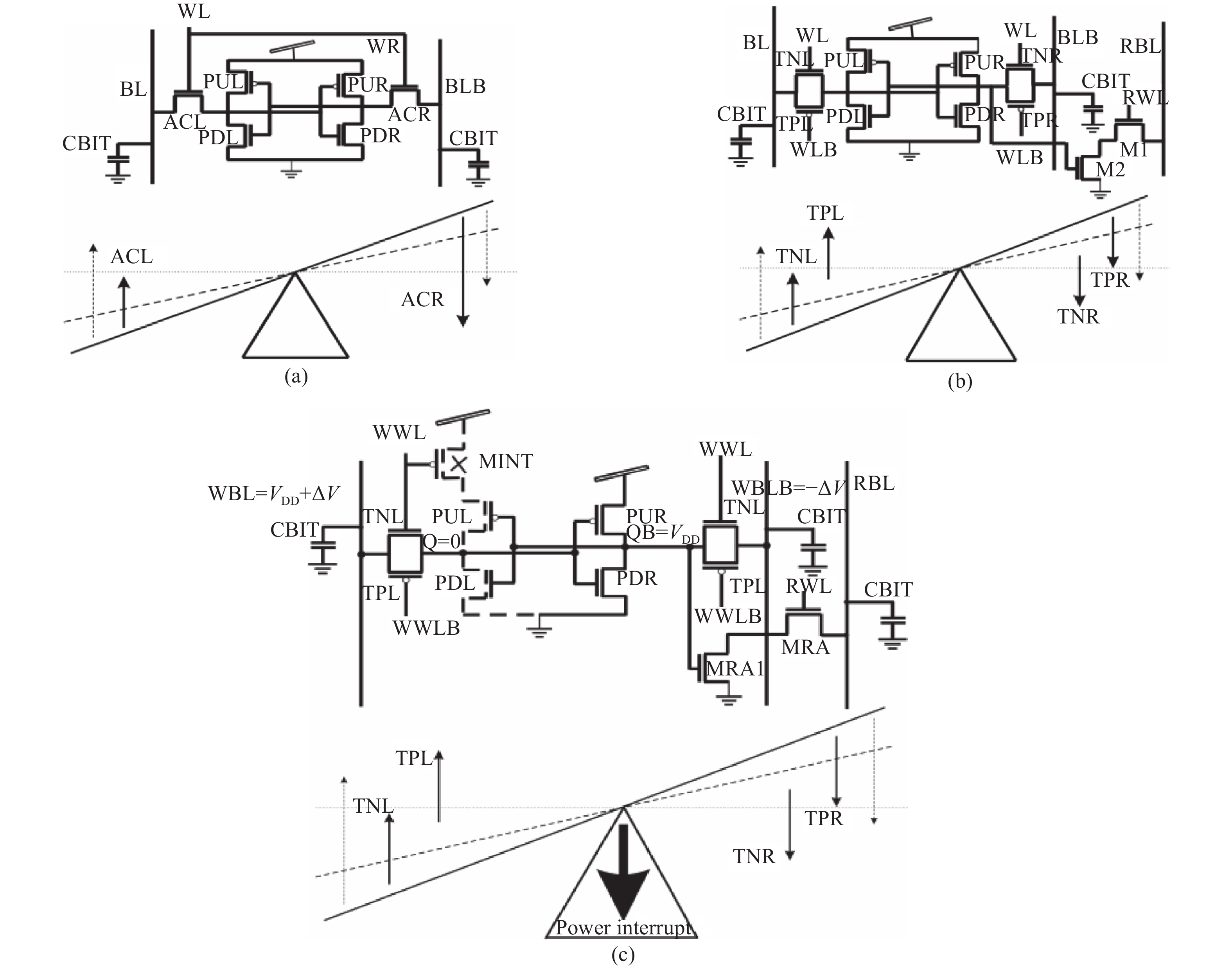
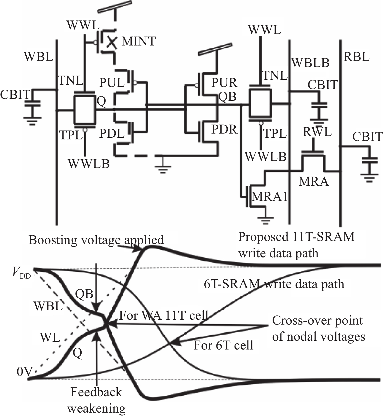
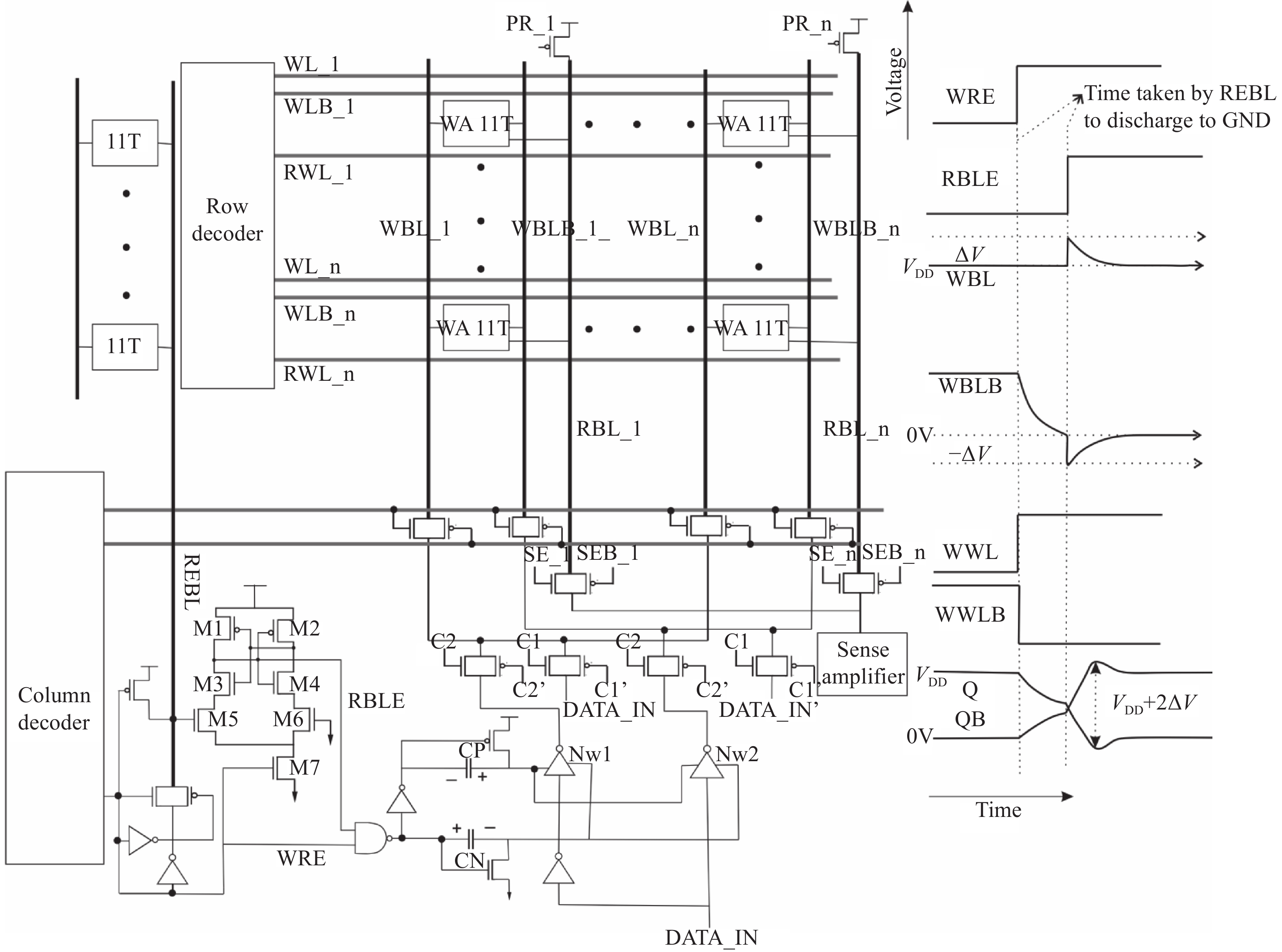
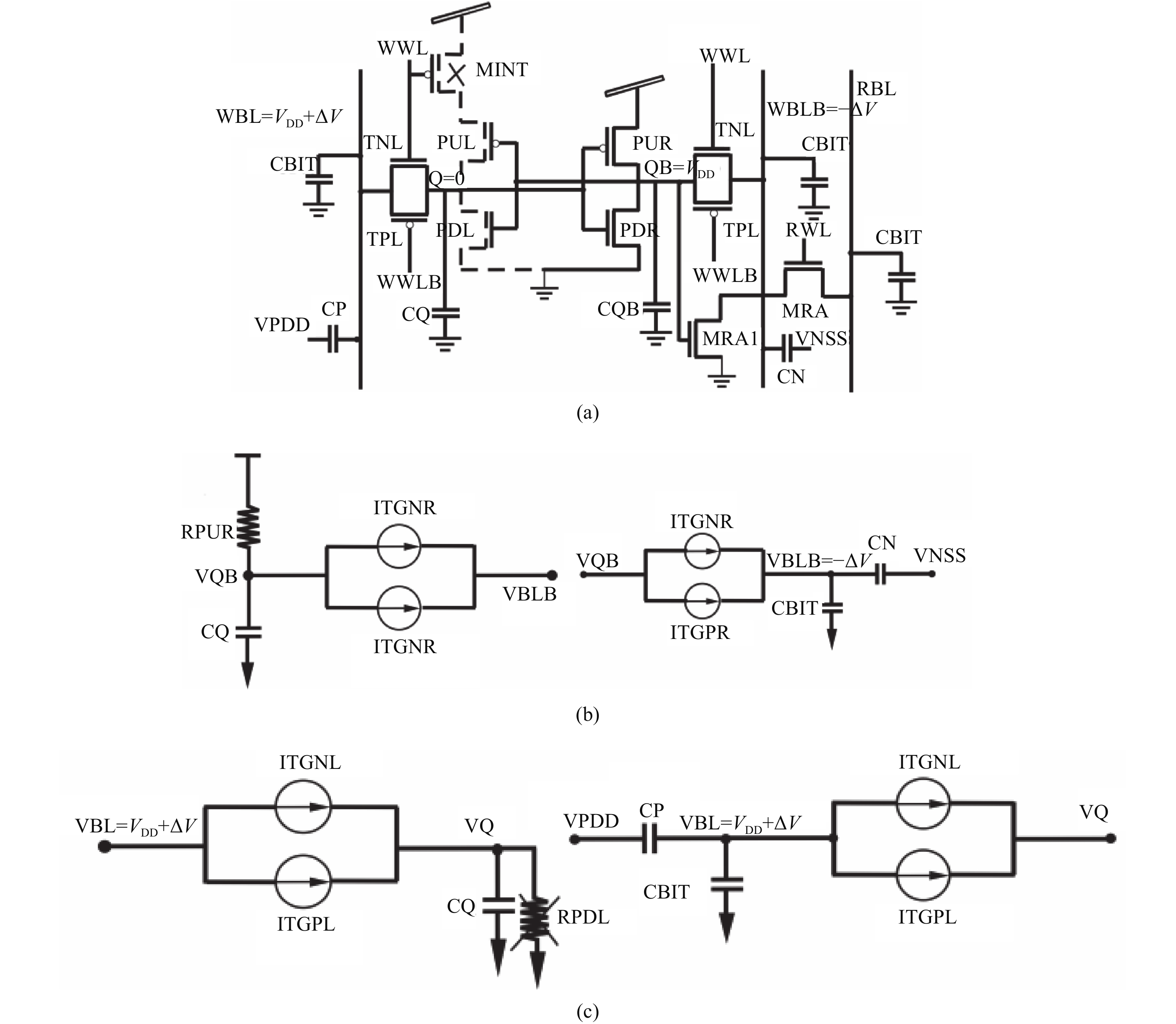
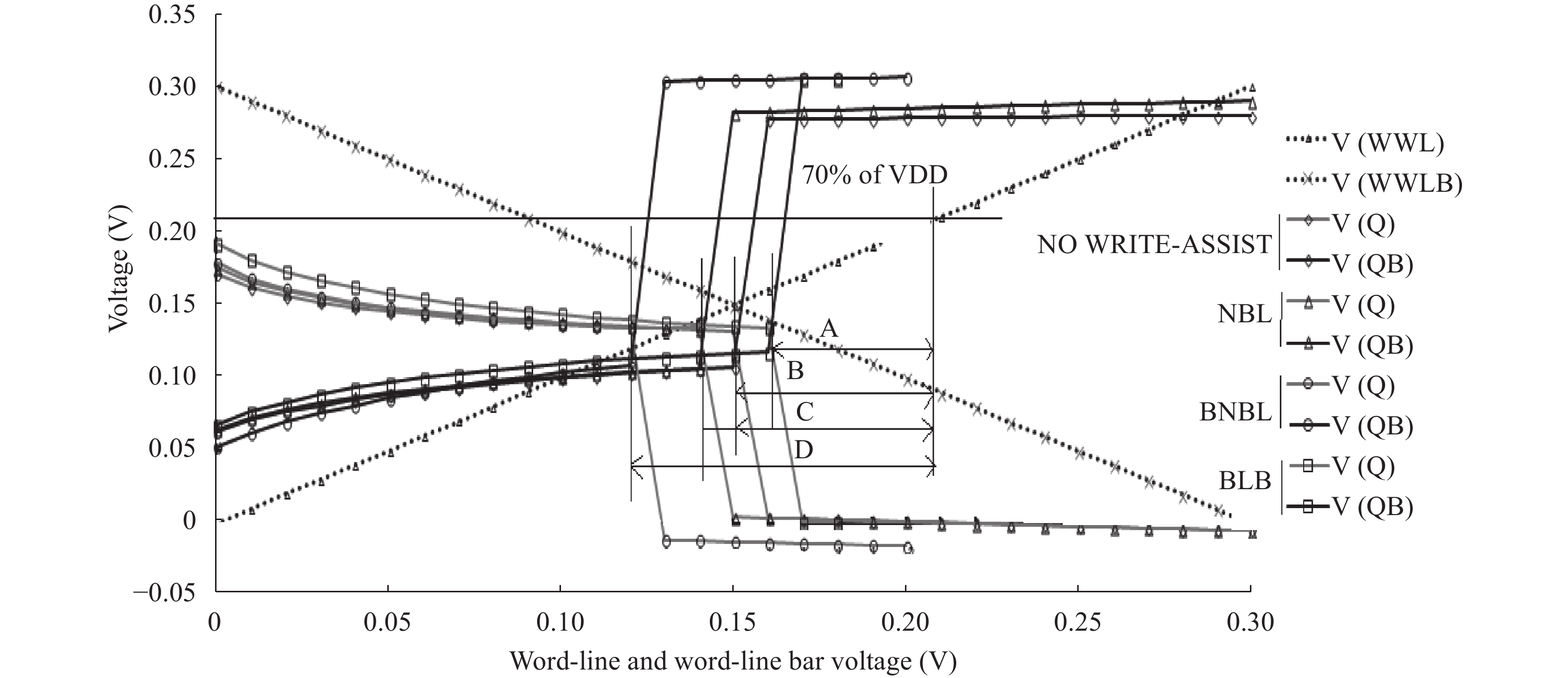
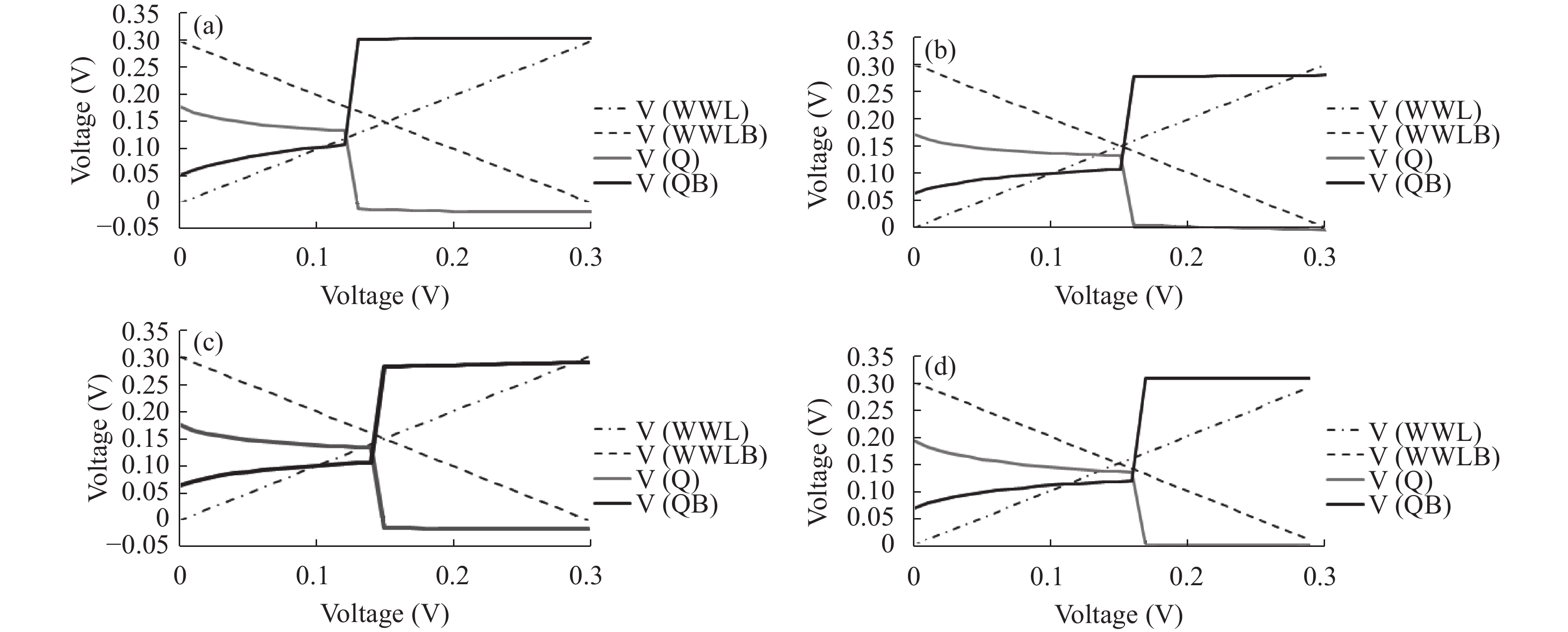
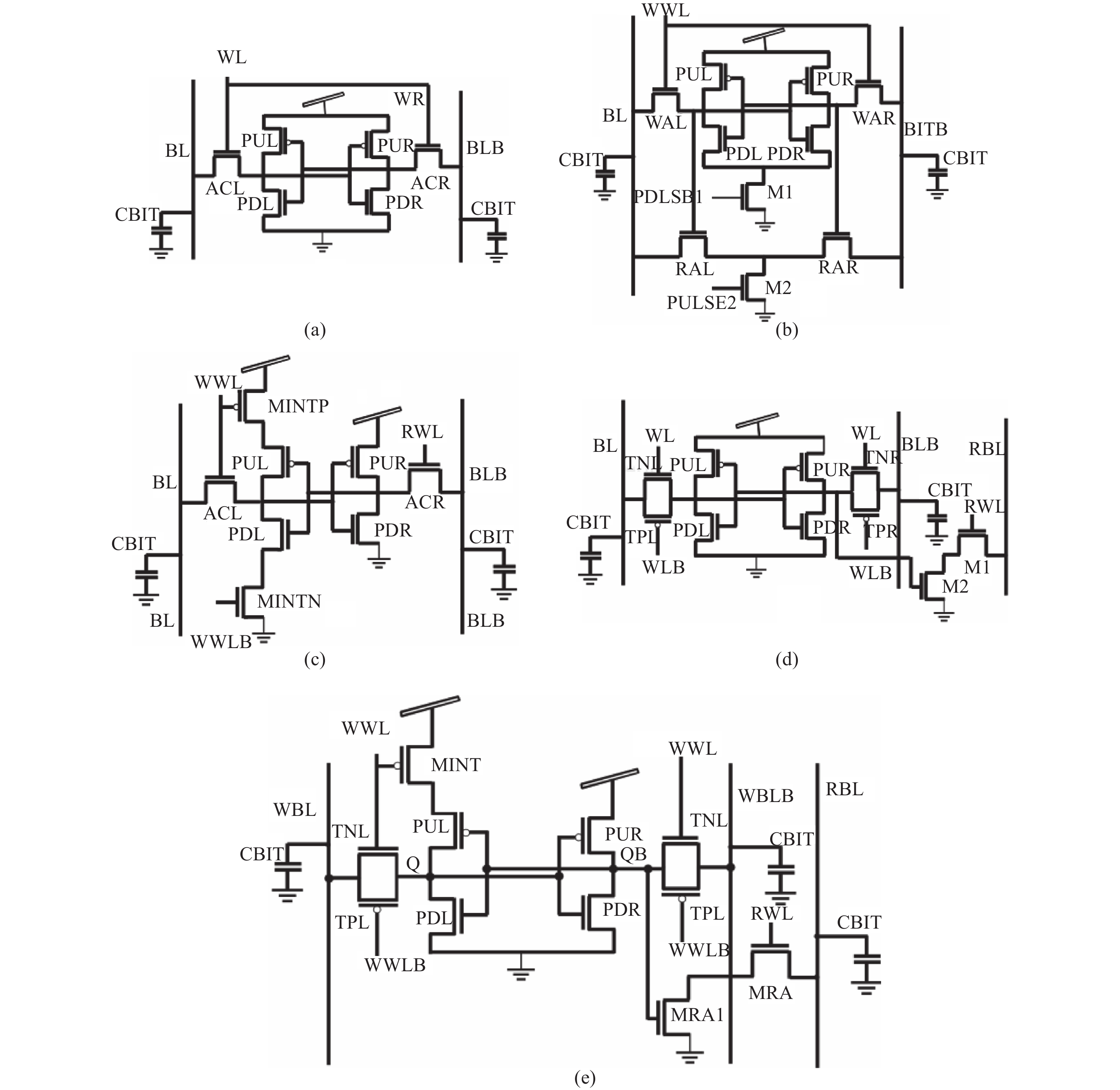
A new 11 T SRAM cell with write-assist is proposed to improve operation at low supply voltage. In this technique, a negative bit-line voltage is applied to one of the write bit-lines, while a boosted voltage is applied to the other write bit-line where transmission gate access is used in proposed 11 T cell. Supply voltage to one of the inverters is interrupted to weaken the feedback. Improved write feature is attributed to strengthened write access devices and weakened feedback loop of cell at the same time. Amount of boosting required for write performance improvement is also reduced due to feedback weakening, solving the persistent problem of half-selected cells and reliability reduction of access devices with the other suggested boosted and negative bit-line techniques. The proposed design improves write time by 79%, 63% and slower by 52% with respect to LP 10 T, WRE 8 T and 6 T cells respectively. It is found that write margin for the proposed cell is improved by about 4×, 2.4× and 5.37× compared to WRE8 T, LP10 T and 6 T respectively. The proposed cell with boosted negative bit line (BNBL) provides 47%, 31%, and 68.4% improvement in write margin with respect to no write-assist, negative bit line (NBL) and boosted bit line (BBL) write-assist respectively. Also, new sensing circuit with replica bit-line is proposed to give a more precise timing of applying boosted voltages for improved results. All simulations are done on TSMC 45 nm CMOS technology. -
References
[1] Chandrakasan A, Daly D C, Finchelstein D F, et al. Technologies for ultradynamic voltage scaling. Proc IEEE, 2010, 98(2): 191 doi: 10.1109/JPROC.2009.2033621[2] Moradi F, Gupta S K, Panagopoulos G, et al. Asymmetrically doped FinFETs for low-power robust SRAMs. IEEE Trans Electron Devices, 2011, 58(12): 4241 doi: 10.1109/TED.2011.2169678[3] Lo C H, Haung S Y. P–P–N based 10T RAM cell for low-leakage and resilient subthreshold operation. IEEE Trans JSSC, 2011, 46(3): 695[4] Agarwal A, Hsu S, Mathew S, et al. A 32 nm 8.3 GHz 64-entry 32b variation tolerant near-threshold voltage register file. IEEE Symposium on VLSI Circuits (VLSIC), 2010: 105[5] Verma N, Chandrakasan A. A 256 kb 65 nm 8T subthreshold SRAM employing sense-amplifier redundancy. IEEE J Solid-State Circuits, 2008, 43(1): 141 doi: 10.1109/JSSC.2007.908005[6] Aly R E, Bayoumi M A. Low-power cache design using 7 T SRAM cell. IEEE Trans Circuits Syst II, 2007, 54(4): 318 doi: 10.1109/TCSII.2006.877276[7] Zhang K, Hamzaoglu F, Wang Y. Low-power SRAMs in nanoscale CMOS technologies. IEEE Trans Electron Devices, 2008, 55(1): 145 doi: 10.1109/TED.2007.911356[8] Pasandi G, Fakhraie S M. A new sub-threshold 7 T SRAM cell design with capability of bit-interleaving in 90 nm CMOS. Proc 21st ICEE, 2013: 1[9] Pasandi G, Fakhraie S M. An 8T low-voltage and low-leakage half-selection disturb-free SRAM using bulk-CMOS and FinFETs. IEEE Trans Electron Devices, 2014, 61(7): 2357 doi: 10.1109/TED.2014.2321295[10] Islam A, Hasan M. Leakage characterization of 10 T SRAM cell. IEEE Trans Electron Devices, 2012, 59(3): 631 doi: 10.1109/TED.2011.2181387[11] Mehrabi K, Ebrahimi B, Afzali-Kusha A. A robust and low power 7 T SRAM cell design. 18th CSI International Symposium on Computer Architecture and Digital Systems (CADS), 2015: 1[12] Liu Z, Kursun V. Characterization of a novel nine-transistor SRAM cell. IEEE Trans Very Large Scale Integr (VLSI) Syst, 2008, 16(4): 488 doi: 10.1109/TVLSI.2007.915499[13] Wang Y, Karl E, Meterelliyoz M, et al. Dynamic behaviour of SRAM data retention and a novel transient voltage collapse technique for 0.6 V 32 nm LP SRAM. IEDM Digest of Technical Papers, 2011: 741[14] Yamaoka M, Maeda N, Shinozaki Y, et al. Low-power embedded SRAM modules with expanded margins for writing. ISSCC Digest of Technical Papers, 2005: 480[15] Karl E, Wang Y, Ng Y G, et al. A 4.6 GHz 162 Mb SRAM design in 22 nm tri-gate CMOS technology with integrated active VMIN-enhancing assist circuitry. ISSCC Digest of Technical Papers, 2012: 230[16] Yabuuchi M, Nii K, Tsukamoto Y, et al. 45 nm 0.6 V cross-point 8 T SRAM with negative biased read/write assist. Proceedings of the IEEE Symposium on VLSI Circuits, 2009: 158[17] Mukhopadhyay S, Rao R M, Kim J J, et al. SRAM write-ability improvement with transient negative bit-line voltage. IEEE Trans VLSI Syst, 2011, 19(1): 24 doi: 10.1109/TVLSI.2009.2029114[18] Chang J, Chen Y H, Cheng H, et al. A 20 nm 112 Mb SRAM in high-κ metal-gate with assist circuitry for low-leakage and low-VMIN applications. SSCC Digest of Technical Papers, 2013: 316[19] Farkhani H, Peiravi A, Moradi F. A new write assist technique for SRAM design in 65 nm CMOS technology. Integration, The VLSI Journal, 2015, 50: 16 doi: 10.1016/j.vlsi.2015.01.001[20] Collaert N, Keersgieter A D, Dixit A, et al. Multigate devices for the 32 nm technology node and beyond. Proceedings of the 37th ESSRDERC, 2007: 143[21] Fujimura Y, Hirabayashi O, Sasaki T, et al. A configurable SRAM with constant negative level write buffer for low voltage operation with 0.149 mm2 cell in 32 nm high-k metal-gate CMOS. ISSCC Digest of Technical Papers, 2010: 348[22] Moradi F, Wisland D T, Aunet S, et al. 65 nm sub-threshold 11 T-SRAM for ultra low voltage applications. SOC Conference, IEEE International, 2008: 113[23] Zimmer B, Toh S O, Vo H, et al. SRAM assist techniques for operation in a wide voltage range in 28 nm CMOS. IEEE Trans Circuits Syst II, 2012, 59(12): 853 doi: 10.1109/TCSII.2012.2231015[24] Moradi F, Panagopoulos G, Karakonstantis G, et al. Multi-level word line driver for robust SRAM design in nano-scale CMOS technology. Microelectron J, 2014, 45(1): 23 doi: 10.1016/j.mejo.2013.09.009[25] Wang J, Nalam S, Calhoun B H. Analyzing static and dynamic write margin for nanometer SRAMs. Proceedings of the International Symposium on Low Power Electronics and Design, 2008: 129[26] Chang I J, Kim J J, Park S P, et al. A 32 kb 10 T sub-threshold SRAM array with bit-interleaving and differential read scheme in 90 nm CMOS. IEEE Trans JSSC, 2009, 44(2): 650 -
Proportional views


 DownLoad:
