| [1] |
Nakamura S, Senoh M, Iwasa N, et al. High-power InGaN single-quantum-well-structure blue and violet light-emitting diodes. Appl Phys Lett, 1995, 67(13): 1868 doi: 10.1063/1.114359 |
| [2] |
Qi C L, Huang Y, Zhan T, et al. Fabrication and characteristics of excellent current spreading GaN-based LED by using transparent electrode–insulator–semiconductor structure. J Semicond, 2017, 38(8): 084005 doi: 10.1088/1674-4926/38/8/084005 |
| [3] |
Keller S, Li H, Laurent M, et al. Recent progress in metal–organic chemical vapor deposition of N-polar group-III nitrides. Semicond Sci Technol, 2014, 29(11): 113001 doi: 10.1088/0268-1242/29/11/113001 |
| [4] |
Mita S. Polarity control in GaN epilayers grown by metalorganic chemical vapor deposition. Master‘s Thesis, North Carolina State University, 2007
|
| [5] |
Liu B, Zhang S, Yin J Y, et al. Effect of high-temperature buffer thickness on quality of AlN epilayer grown on sapphire substrate by metalorganic chemical vapor deposition. Chin Phys B, 2013, 22(5): 057105 doi: 10.1088/1674-1056/22/5/057105 |
| [6] |
Mohn S, Stolyarchuk N, Markurt T, et al. Polarity control in group-III nitrides beyond pragmatism. Phys Rev Appl, 2016, 5(5): 054004 doi: 10.1103/PhysRevApplied.5.054004 |
| [7] |
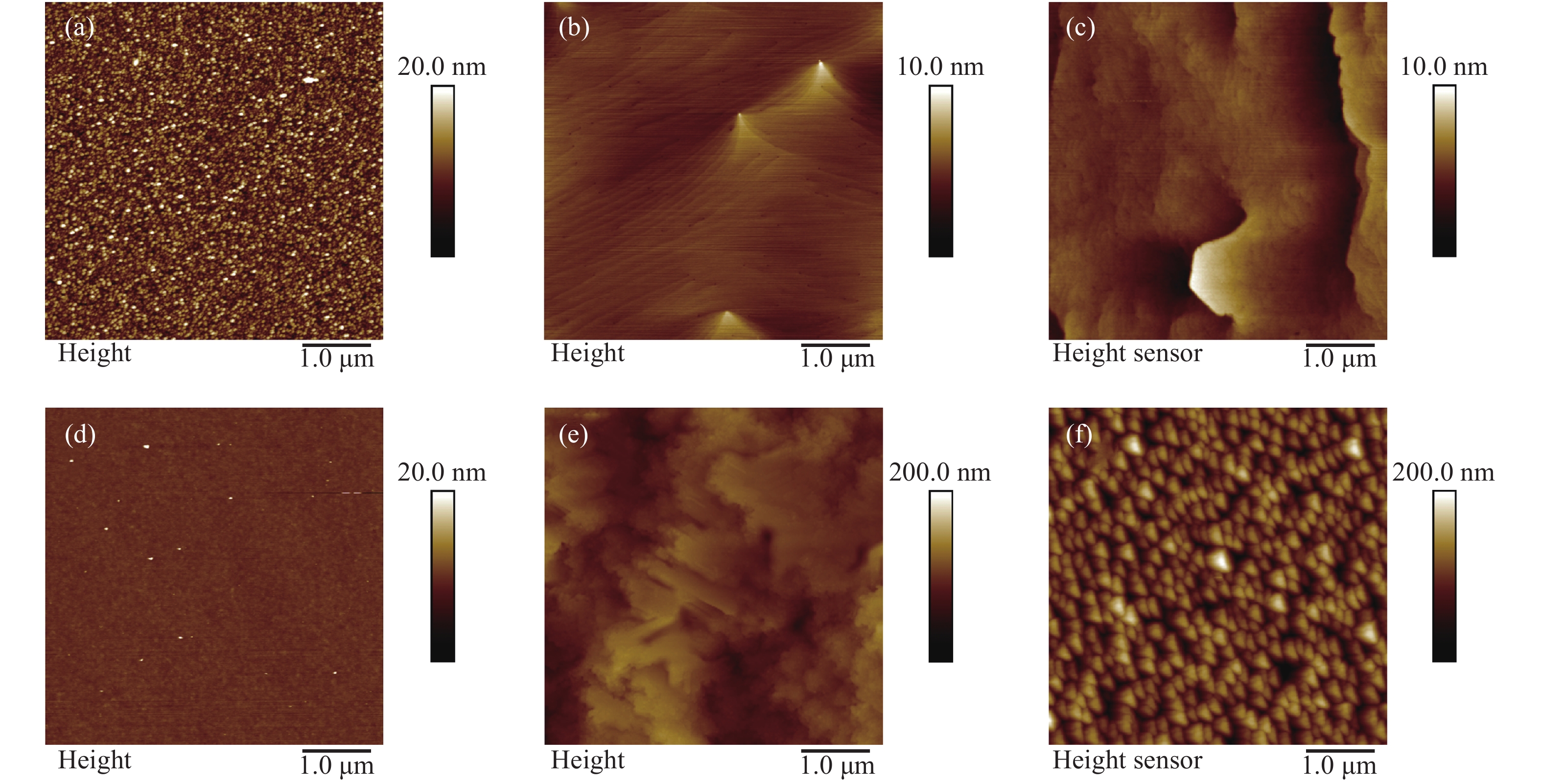
Rice A, Collazo R, Tweedie J, et al. Surface preparation and homoepitaxial deposition of AlN on (0001)-oriented AlN substrates by metalorganic chemical vapor deposition. J Appl Phys, 2010, 108(4): 043510 doi: 10.1063/1.3467522 |
| [8] |
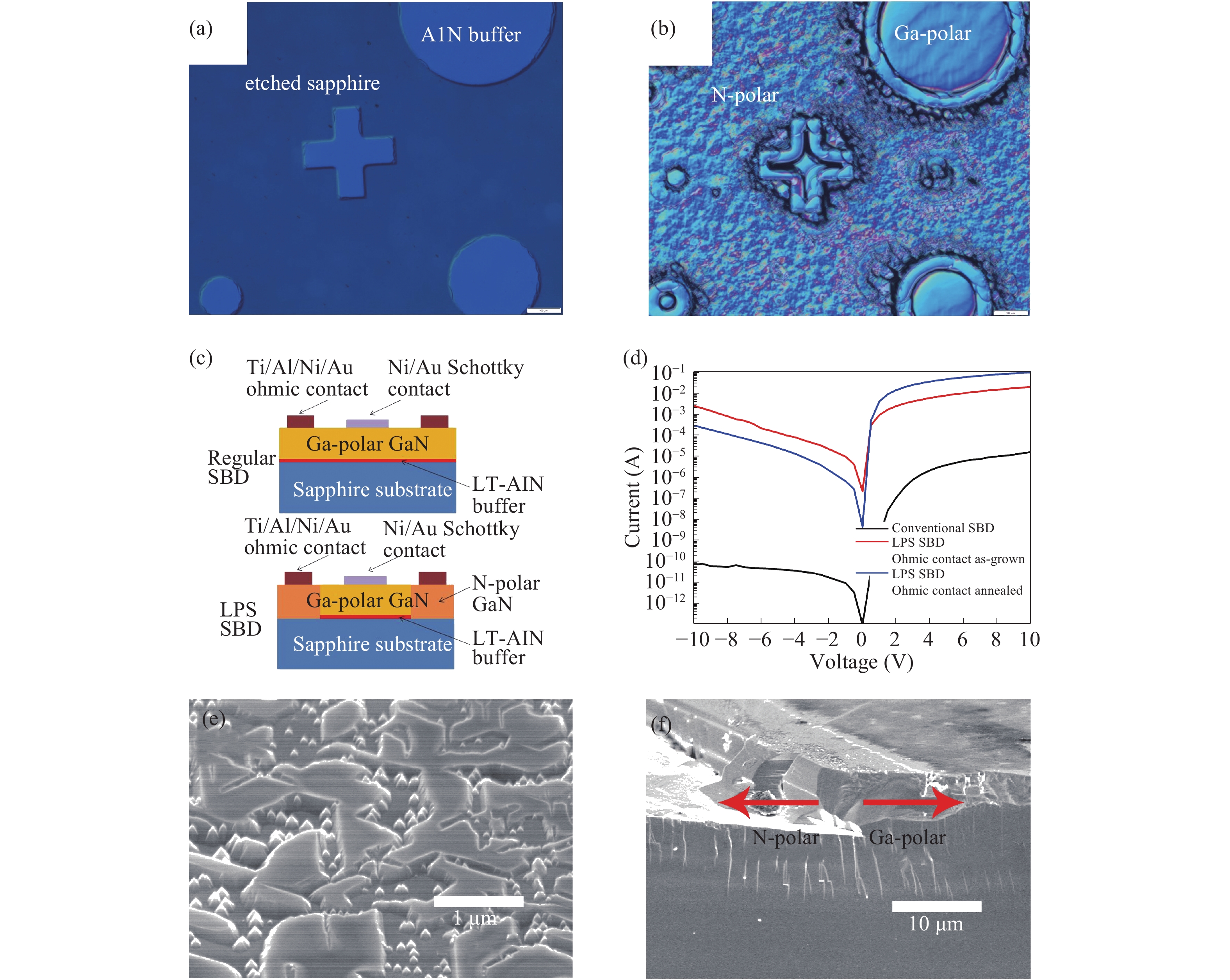
Hite J K, Zoll R, Mastro M A, et al. Role of growth parameters in equalizing simultaneous growth of N-and Ga-polar GaN by MOCVD. Phys Status Solidi C, 2014, 11(3/4): 458
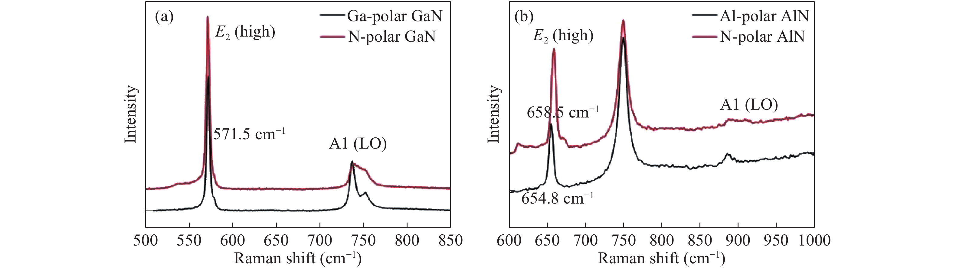
|
| [9] |
Collazo R N, Mita S, Xie J, et al. Implementation of the GaN lateral polarity junction in a MESFET utilizing polar doping selectivity. Phys Status Solidi A, 2010, 207(1): 45 doi: 10.1002/pssa.v207:1 |
| [10] |
Alden D, Guo W, Kirste R, et al. Fabrication and structural properties of AlN submicron periodic lateral polar structures and waveguides for UV-C applications. Appl Phys Lett, 2016, 108(26): 261106 doi: 10.1063/1.4955033 |
| [11] |
Troha T, Rigler M, Alden D, et al. UV second harmonic generation in AlN waveguides with modal phase matching. Opt Mater Express, 2016, 6(6): 2014 doi: 10.1364/OME.6.002014 |
| [12] |
Losurdo M, Giangregorio M M, Capezzuto P, et al. Interplay between GaN polarity and surface reactivity towards atomic hydrogen. J Appl Phys, 2004, 95(12): 8408 doi: 10.1063/1.1745124 |
| [13] |
Bryan I, Bryan Z, Mita S, et al. Surface kinetics in AlN growth: a universal model for the control of surface morphology in III-nitrides. J Cryst Growth, 2016, 438: 81 doi: 10.1016/j.jcrysgro.2015.12.022 |
| [14] |
Sun Q, Cho Y, Lee I H, et al. Nitrogen-polar GaN growth evolution on c-plane sapphire. Appl Phys Lett, 2008, 93(13): 131912 doi: 10.1063/1.2993333 |
| [15] |
Guo W, Kirste R, Bryan I, et al. KOH based selective wet chemical etching of AlN, Al xGa 1−xN, and GaN crystals: a way towards substrate removal in deep ultraviolet-light emitting diode. Appl Phys Lett, 2015, 106(8): 082110 doi: 10.1063/1.4913705 |
| [16] |
|
| [17] |
Haboeck U, Siegle H, Hoffmann A, et al. Lattice dynamics in GaN and AlN probed with first-and second-order Raman spectroscopy. Phys Status Solidi C, 2003, 0(6): 1710 doi: 10.1002/pssc.200303130 |
| [18] |
Tian Y, Zhang Y, Yan J, et al. Stimulated emission at 272 nm from an Al xGa 1−xN-based multiple-quantum-well laser with two-step etched facets. RSC Adv, 2016, 6(55): 50245 doi: 10.1039/C6RA11612D |
| [19] |
Kirste R, Mita S, Hussey L, et al. Polarity control and growth of lateral polarity structures in AlN. Appl Phys Lett, 2013, 102(18): 181913 doi: 10.1063/1.4804575 |
| [20] |
Guo W, Xie J, Akouala C, et al. Comparative study of etching high crystalline quality AlN and GaN. J Cryst Growth, 2013, 366: 20 doi: 10.1016/j.jcrysgro.2012.12.141 |
| [21] |
Bryan I, Bryan Z, Mita S, et al. The role of surface kinetics on composition and quality of AlGaN. J Cryst Growth, 2016, 451: 65 doi: 10.1016/j.jcrysgro.2016.06.055 |
| [22] |
Wang T Y, Tasi C T, Lin C F, et al. 85% internal quantum efficiency of 280-nm AlGaN multiple quantum wells by defect engineering. Sci Rep, 2017, 7(1): 14422 doi: 10.1038/s41598-017-14825-8 |
| [23] |
Hoffmann M P, Kirste R, Mita S, et al. Growth and characterization of Al xGa 1−xN lateral polarity structures. Phys Status Solidi A, 2015, 212(5): 1039 doi: 10.1002/pssa.v212.5 |


 DownLoad: