Processing math: 100%
J. Semicond. > 2018, Volume 39 > Issue 5 > 053004

SEMICONDUCTOR MATERIALS

Growth and characteristics of p-type doped GaAs nanowire

Bang Li, Xin Yan, Xia Zhang and Xiaomin Ren

+ Author Affiliations

 Corresponding author: Bang Li, libang@bupt.edu.cn

DOI: 10.1088/1674-4926/39/5/053004

PDF

Turn off MathJax

Abstract: The growth of p-type GaAs nanowires (NWs) on GaAs (111) B substrates by metal-organic chemical vapor deposition (MOCVD) has been systematically investigated as a function of diethyl zinc (DEZn) flow. The growth rate of GaAs NWs was slightly improved by Zn-doping and kink is observed under high DEZn flow. In addition, the IV curves of GaAs NWs has been measured and the p-type dope concentration under the II/III ratio of 0.013 and 0.038 approximated to 1019–1020 cm−3.

Key words: nanowireGaAsp-dopedVLS

Recently, III–V semiconductor nanowires (NW) have attracted great research interest due to their superior electrical and optoelectronic properties for future high performance nanoscaled devices, such as photodetector, solar cell, nanolaser, and light-emitting diode[17]. The future of all semiconductor NW technology will inherently rely on their doping capability. Both n- and p-type doping of NWs play important roles in most optoelectronic applications, since these applications are fabricated by the barriers such as pn junction[8]. Different from the growth of film structures, it is recognized that NW growth is initiated by a supersaturated liquid alloy through the vapor–liquid–solid (VLS) mechanism[9]. However, the question of doping mechanism still remains unsolved. It is not clear whether the dopants accumulate within the catalyst or they undergo diffusion mechanism from the sidewalls[10]. In addition, the typical NW growth conditions often do not favor dopant incorporation. There are only a very few publications describing the growth of p-type GaAs NWs[11, 12]. The widely used method of p-type doping in metal-organic chemical vapor deposition (MOCVD) is adding diethyl zinc (DEZn) to the gas phase during growth. It is reported that the doping concentrations are controlled from 4.6 × 10¹⁸ up to 2.3 × 1019 cm−3 by adjusting the II/III ratio[22]. In this paper, we report on p-type doping of GaAs nanowires realized by an additional DEZn flow during the growth. The IV curves of NWs were measured and the doping concentration approximated to 1019–1020 cm−3.

The growth was carried out in a Thomas Swan close-coupled showerhead-metal-organic chemical vapor deposition (CCS-MOCVD) reactor at the pressure of 100 Torr. Before the growth, an Au film with a thickness of 4 nm was deposited on GaAs (111) B substrate by magnetron sputtering; the Au-coated GaAs substrate was placed in the reactor and annealed in situ at 645 °C in ambient arsine (AsH3) for 900 s to form the Au–Ga alloyed particles as catalyst. Trimethylgallium (TMGa) and AsH3 were used as precursors. The doping source was DEZn and hydrogen (H2) served as the carrier gas. GaAs NWs growth began after it was ramped down to the desired temperature. GaAs NWs were grown at 490 °C for 2000 s. The input II/III ratio was adjusted by varying the DEZn flow while keeping the TMGa flow constant at 14.4 sccm and the AsH3 at 100 sccm. After growth, the samples were cooled down in ambient H2. Five samples were grown in the experiment. The dopant to TMGa (II/III ratio) in the samples was varied in the range of 0.013 ≤ II/III ≤ 0.05.

As-grown nanowires were then transferred onto an intrinsic Si substrate that was covered with a 500 nm SiO2 layer by sonication with ethanol as carrier. Then electrodes were defined on both ends of a chosen NW by UV lithography and electromagnetic sputtering followed by a “lift-off” process. Before sputtering, the unmasked contact areas were etched for 5 s, and then passivated with (NH4)2S solution[1315]. The morphological and structural characteristics of the samples were characterized by scanning electron microscopy (SEM) and the current–voltage (IV) measurements were performed with an Agilent 2901A source meter. A 532 nm continuous-wave diode-pumped solid-state (DPSS) laser was used to excite the device.

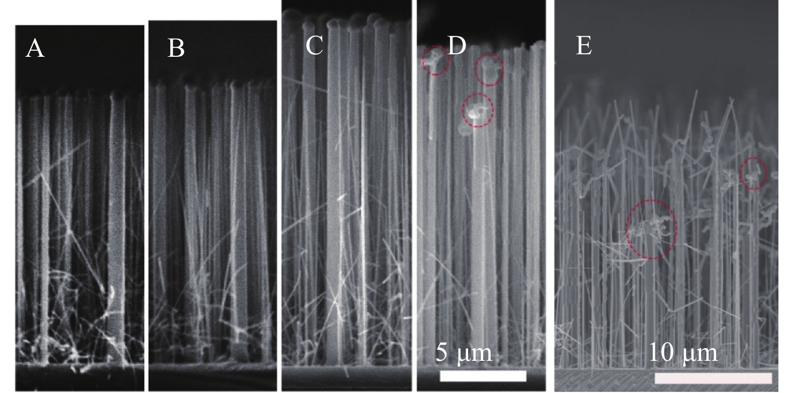
Figs. 1(a)1(e) show the cross-sectional SEM images of samples A–E, respectively. The DEZn flow during the growth of these samples increased from 5 sccm (A) to 20 sccm (E) as shown in Table 1. That is, the II/III ratio changed from 0.013 to 0.05. The average length of NWs for sample A, B, and C is 15.5, 16.1 and 20.0 μm, corresponding to the growth rate of 7.8, 8.1, and 10 nm/s, respectively. The increased growth rate with increasing the II/III ratio indicates that the enhanced flow of DEZn has a slight promoting effect on the growth rate of GaAs NWs. The reason is that DEZn, which predominantly decomposes heterogeneously, passivates the bare GaAs surface by a partial coverage of non-decomposed DEZn molecules and thereby increases the kinetic energy barrier for the growth of NW[16]. Besides, when DEZn flow is high (i.e. 15 sccm), a kink is observed on the top of NW which is marked by the red dotted circle in sample D. Kinking enhanced with the increased II/III ratio since the higher Zn concentration in the droplet destroyed the stabilization of the surface energy of the droplet. Moreover, the droplet split up under the II/III ratio of 0.05 (sample E), thus brand is observed on the top of NWs as shown in Fig. 1(e).

Figure  1.  The SEM image of all the samples. The growth parameters of each sample are shown in Table 1.
Table  1.  The growth parameters of all samples.
Sample DEZn
flow (sccm)
AsH3
flow (sccm)
TMGa
flow (sccm)
II/III ratio Growth
temperature (°C)
Growth
time (s)
Height
(μm)
A 5 100 14.4 0.013 490 2000 15.5
B 10 100 14.4 0.025 490 2000 16.1
C 12.5 100 14.4 0.031 490 2000 20.0
D 15 100 14.4 0.038 490 2000 17–18
E 20 100 14.4 0.05 490 2000
DownLoad: CSV  | Show Table

The widely accepted growth model is the vapor–liquid–solid (VLS) mechanism. In the VLS mechanism, it is assumed that the NW growth can be controlled by the direct impingement of growth material from the gas phase onto the catalyst droplet. Furthermore, the changed nanowire growth direction during growth could be understood from the kinetic coefficients of crystallization based on the theory of nucleation at constant supersaturation in eutectic droplets. The influence of the composition of the catalyst droplet may change the liquid-vapor interfacial energy. In our experiment, the interfacial energy is changed by the doping of Zn. The changed interfacial energy makes it possible for the droplet to unpin from the nanowire tip during the growth. As the atoms grow layer-by-layer on the top of NW, the displacement of the droplets may occur in the growth of every layer of atoms. When the liquid droplet unpins, it moves onto a sidewall (111) facet, and continues to grow, thus forming a kink. It is observed that the probability of the displacement of the droplet increases with the concentration of Zn in the droplet, thus kinking enhanced with the increased II/III ratio.

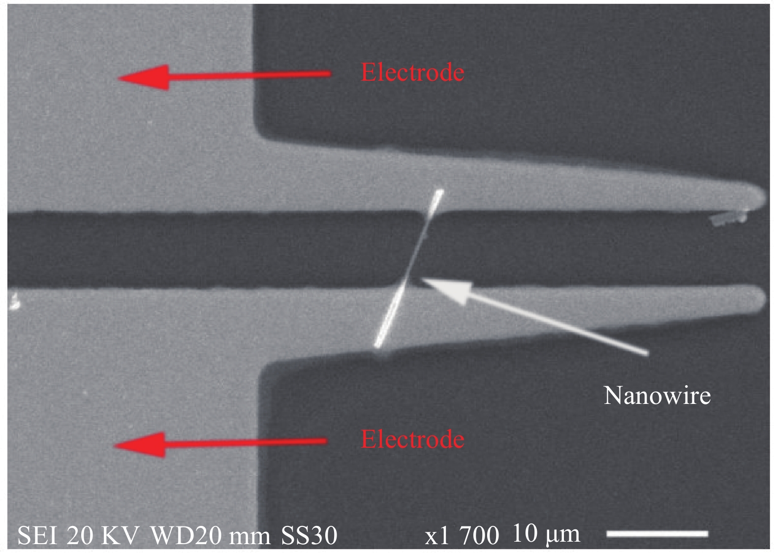
To estimate the doping concentration of Zn in the GaAs NWs, the IV curves of NWs were measured by the device of NWs between two Pt/Ti/Pt/Au (200 nm) ohmic contacted electrodes. Fig. 2 shows the SEM image of the device. The measurement was divided into two groups in which the NWs came from sample A and sample D, respectively. Fig. 3 shows the IV curves of the two groups. All the devices show a linear hole transfer characteristic due to the ohmic contact. Although the resistances of NWs should change with the doping concentration, it is hard to show the doping concentration from the IV curves. This is because the NWs in each group have different diameters and lengths, the resistances of each NW are different even in the same group. To calculate the doping concentration, the conductivity needs to be calculated by the measured parameters of each samples such as the length of conductive channel and the diameter of each NW. The diameters and lengths are measured in the SEM image of each device and the resistance is calculated from Fig. 3. The morphology parameters and estimation resistance of these measured GaAs NWs are shown in Table 2. Taking these parameters into consideration, the conductivity can be calculated by Eq. (1):

Figure  2.  SEM image of the measured device.
Figure  3.  (Color online) (a) IV curves of NWs from sample A. (b) IV curves of NWs from sample D.
Table  2.  Morphology parameters and estimation resistance of these measured GaAs NWs.
Sample Diameter (nm) Length (μm) Resistance (Ω)
A1 340 6.59 1700
A2 890 5.9 120
A3 200 6.47 6500
D1 650 7.27 440
D2 345 6.68 2020
D3 300 5.88 2290
D4 150 6.5 430 000
DownLoad: CSV  | Show Table
σ=lRs. (1)

Thus, the doping concentration NA[1720] can be estimated by Eq. (2) and Eq. (3)[2123]:

σ=pqμp,GaAs, (2)
μp,GaAs=μp01+NA1018 cm3, (3)

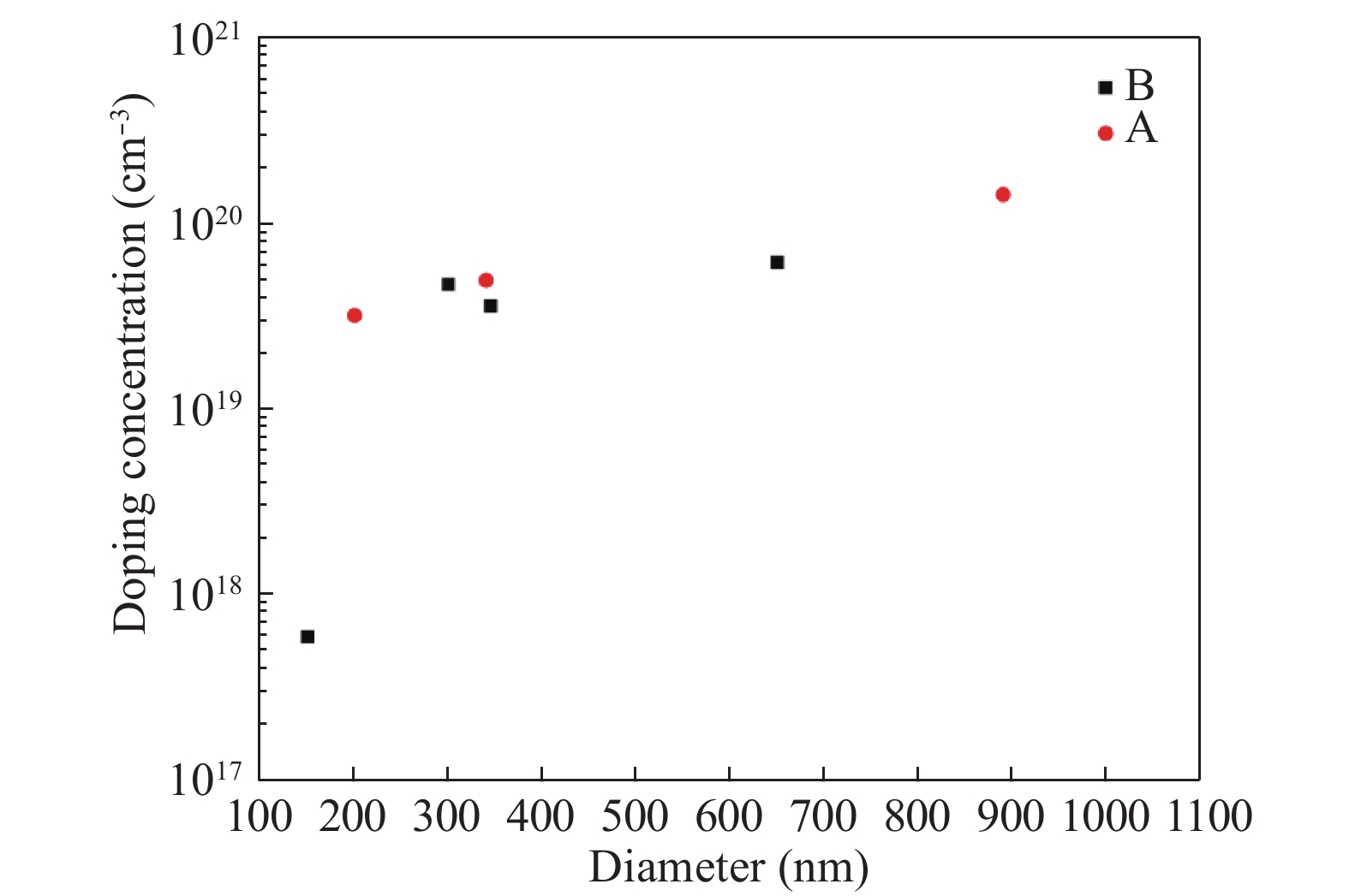
where p is the hole concentration in the NW which approximates the doping concentration NA, μp, GaAs is the GaAs mobility with doping, μp0 is the GaAs mobility without doping which is estimated as 450 cm2/(V·s)[23, 24]. The estimation results are shown in Fig. 4. It is observed that the p-type dope concentrations under the II/III ratio of 0.013 (A) and 0.038 (B) approximate to 1019–1020 cm−3. The estimated value will be higher if the GaAs mobility without doping is used as the hole mobility of GaAs NW which is several tens of cm2/(V·s)[23, 24]. It is reported that the doping concentration increased with the enhanced diameter, which is consistent with that in our experiment[23]. Besides, it is also reported that the doping concentration increased with the enhanced II/III ratio during the unkinked growth[23]. However, when the NWs exhibit kink under high II/III ratio (sample D) due to the increased Zn in the droplet, the doping concentration seems almost unchanged compared with the low II/III ratio (sample A). That is, although the NW kinked by increasing the flow of DEZn, the high concentration of Zn in the droplet has little influence on the doping concentration. Nevertheless, the fabrication of the NW with high doping concentration that has a more stable droplet under high II/III ratio during growth still needs future investigations.

Figure  4.  (Color online) The calculated doping concentrations of measured NWs.

In summary, p-type doping using DEZn as doping precursor during the VLS growth of GaAs nanowires was demonstrated. The II/III ratio in the samples varied in the range of 0.013–0.05. Stronger kink of the NWs with increasing DEZn flow gives evidence that Zn is incorporated via VLS mechanism, and it also indicates an upper limit of p-type doping. IV characteristic of NWs that shows a linear dependence and the morphology parameters of measured NWs is obtained from the SEM image. Calculating by these parameters, the p-type dope concentration under the II/III ratio of 0.013 and 0.038 approximated to 1019–1020 cm−3. The p-type doping of nanowires is of general interest for all compound semiconductor nanowires. What is more, the high doping concentration of NW will play an essential role in future applications of optoelectronics and sensor technologies.


[1]
Dai X, Zhang S, Wang Z, et al. GaAs/AlGaAs nanowire photodetector. Nano Lett, 2014, 14(5): 2688 doi: 10.1021/nl5006004
[2]
Tsakalakos L, Balch J, Fronheiser J, et al. Silicon nanowire solar cells. Appl Phys Lett, 2007, 91(23): 233117 doi: 10.1063/1.2821113
[3]
Piccione B, Cho C, Vugt L K, et al. All-optical active switching in individual semiconductor nanowires. Nat Nanotechnol, 2012, 7: 640 doi: 10.1038/nnano.2012.144
[4]
Pan C, Dong L, Zhu G, et al. High-resolution electroluminescent imaging of pressure distribution using a piezoelectric nanowire LED array. Nat Photonics, 2013, 7(9): 752 doi: 10.1038/nphoton.2013.191
[5]
Hoa N D, Le D T T, Tam P D, et al. On-chip fabrication of SnO2-nanowire gas sensor: The effect of growth time on sensor performance. Sens Actuator B, 2010, 146(1): 361 doi: 10.1016/j.snb.2010.02.054
[6]
Vitiello M S, Coquillat D, Viti L, et al. Room-temperature terahertz detectors based on semiconductor nanowire field-effect transistors. Nano Lett, 2011, 12(1): 96
[7]
Patolsky F, Zheng G, Lieber C M. Nanowire sensors for medicine and the life sciences. Future Medicine, 2006, 1(1): 51
[8]
Haraguchi K, Katsuyama T, Hiruma K, et al. GaAs p‐n junction formed in quantum wire crystals. Appl Phys Lett, 1992, 60(6): 745 doi: 10.1063/1.106556
[9]
Wagner R S, Ellis W C. Vapor-Liquid-Solid mechanism of single crystal growth. Appl Phys Lett, 1964, 4(5): 89 doi: 10.1063/1.1753975
[10]
Li H Y, Wunnicke O, Borgström M T, et al. Remote p-doping of InAs nanowires. Nano Lett, 2007, 7(5): 1144 doi: 10.1021/nl0627487
[11]
Franke D, Reier F W, Grote N. Post-growth Zn diffusion into InGaAs/InP in a LP-MOVPE reactor. J Cryst Growth, 1998, 195(1–4): 112 doi: 10.1016/S0022-0248(98)00681-2
[12]
Stichtenoth D, Wegener K, Gutsche C, et al. P-type doping of GaAs nanowires. Appl Phys Lett, 2008, 92(16): 163107 doi: 10.1063/1.2912129
[13]
Gutsche C, Niepelt R, Gnauck M, et al. Direct determination of minority carrier diffusion lengths at axial GaAs nanowire p–n junctions. Nano Lett, 2012, 12(3): 1453 doi: 10.1021/nl204126n
[14]
Chang C C, Chi C Y, Yao M, et al. Electrical and optical characterization of surface passivation in GaAs nanowires. Nano Lett, 2012, 12(9): 4484 doi: 10.1021/nl301391h
[15]
Sager D, Gutsche C, Prost W, et al. Recombination dynamics in single GaAs-nanowires with an axial heterojunction: n-versus p-doped areas. J Appl Phys, 2013, 113(17): 174303 doi: 10.1063/1.4803488
[16]
Borgström M T, Norberg E, Wickert P, et al. Precursor evaluation for in situ InP nanowire doping. Nanotechnology, 2008, 19(44): 445602 doi: 10.1088/0957-4484/19/44/445602
[17]
Gutsche C, Lysov A, Regolin I, et al. n-type doping of vapor–liquid–solid grown GaAs nanowires. Nanoscale Res Lett, 2011, 6(1): 65
[18]
Salehzadeh O, Kavanagh K L, Watkins S P. Controlled axial and radial Te-doping of GaAs nanowires. J Appl Phys, 2012, 112(5): 054324 doi: 10.1063/1.4751988
[19]
Joyce H J, Docherty C J, Gao Q, et al. Electronic properties of GaAs, InAs and InP nanowires studied by terahertz spectroscopy. Nanotechnology, 2013, 24(21): 214006 doi: 10.1088/0957-4484/24/21/214006
[20]
Boland J L, Conesa-Boj S, Parkinson P, et al. Modulation doping of GaAs/AlGaAs core–shell nanowires with effective defect passivation and high electron mobility. Nano Lett, 2015, 15(2): 1336 doi: 10.1021/nl504566t
[21]
Sladek K, Klinger V, Wensorra J, et al. MOVPE of n-doped GaAs and modulation doped GaAs/AlGaAs nanowires. J Cryst Growth, 2010, 312(5): 635 doi: 10.1016/j.jcrysgro.2009.11.026
[22]
Sourribes M J L, Isakov I, Panfilova M, et al. Minimization of the contact resistance between InAs nanowires and metallic contacts. Nanotechnology, 2013, 24(4): 045703 doi: 10.1088/0957-4484/24/4/045703
[23]
Gutsche C, Regolin I, Blekker K, et al. Controllable p-type doping of GaAs nanowires during vapor-liquid-solid growth. J Appl Phys, 2009, 105(2): 024305 doi: 10.1063/1.3065536
[24]
Ketterer B, Uccelli E, i Morral A F. Mobility and carrier density in p-type GaAs nanowires measured by transmission Raman spectroscopy. Nanoscale, 2012, 4(5): 1789 doi: 10.1039/c2nr11910b
Fig. 1.  The SEM image of all the samples. The growth parameters of each sample are shown in Table 1.

Fig. 2.  SEM image of the measured device.

Fig. 3.  (Color online) (a) IV curves of NWs from sample A. (b) IV curves of NWs from sample D.

Fig. 4.  (Color online) The calculated doping concentrations of measured NWs.

Table 1.   The growth parameters of all samples.

Sample DEZn
flow (sccm)
AsH3
flow (sccm)
TMGa
flow (sccm)
II/III ratio Growth
temperature (°C)
Growth
time (s)
Height
(μm)
A 5 100 14.4 0.013 490 2000 15.5
B 10 100 14.4 0.025 490 2000 16.1
C 12.5 100 14.4 0.031 490 2000 20.0
D 15 100 14.4 0.038 490 2000 17–18
E 20 100 14.4 0.05 490 2000
DownLoad: CSV

Table 2.   Morphology parameters and estimation resistance of these measured GaAs NWs.

Sample Diameter (nm) Length (μm) Resistance (Ω)
A1 340 6.59 1700
A2 890 5.9 120
A3 200 6.47 6500
D1 650 7.27 440
D2 345 6.68 2020
D3 300 5.88 2290
D4 150 6.5 430 000
DownLoad: CSV
[1]
Dai X, Zhang S, Wang Z, et al. GaAs/AlGaAs nanowire photodetector. Nano Lett, 2014, 14(5): 2688 doi: 10.1021/nl5006004
[2]
Tsakalakos L, Balch J, Fronheiser J, et al. Silicon nanowire solar cells. Appl Phys Lett, 2007, 91(23): 233117 doi: 10.1063/1.2821113
[3]
Piccione B, Cho C, Vugt L K, et al. All-optical active switching in individual semiconductor nanowires. Nat Nanotechnol, 2012, 7: 640 doi: 10.1038/nnano.2012.144
[4]
Pan C, Dong L, Zhu G, et al. High-resolution electroluminescent imaging of pressure distribution using a piezoelectric nanowire LED array. Nat Photonics, 2013, 7(9): 752 doi: 10.1038/nphoton.2013.191
[5]
Hoa N D, Le D T T, Tam P D, et al. On-chip fabrication of SnO2-nanowire gas sensor: The effect of growth time on sensor performance. Sens Actuator B, 2010, 146(1): 361 doi: 10.1016/j.snb.2010.02.054
[6]
Vitiello M S, Coquillat D, Viti L, et al. Room-temperature terahertz detectors based on semiconductor nanowire field-effect transistors. Nano Lett, 2011, 12(1): 96
[7]
Patolsky F, Zheng G, Lieber C M. Nanowire sensors for medicine and the life sciences. Future Medicine, 2006, 1(1): 51
[8]
Haraguchi K, Katsuyama T, Hiruma K, et al. GaAs p‐n junction formed in quantum wire crystals. Appl Phys Lett, 1992, 60(6): 745 doi: 10.1063/1.106556
[9]
Wagner R S, Ellis W C. Vapor-Liquid-Solid mechanism of single crystal growth. Appl Phys Lett, 1964, 4(5): 89 doi: 10.1063/1.1753975
[10]
Li H Y, Wunnicke O, Borgström M T, et al. Remote p-doping of InAs nanowires. Nano Lett, 2007, 7(5): 1144 doi: 10.1021/nl0627487
[11]
Franke D, Reier F W, Grote N. Post-growth Zn diffusion into InGaAs/InP in a LP-MOVPE reactor. J Cryst Growth, 1998, 195(1–4): 112 doi: 10.1016/S0022-0248(98)00681-2
[12]
Stichtenoth D, Wegener K, Gutsche C, et al. P-type doping of GaAs nanowires. Appl Phys Lett, 2008, 92(16): 163107 doi: 10.1063/1.2912129
[13]
Gutsche C, Niepelt R, Gnauck M, et al. Direct determination of minority carrier diffusion lengths at axial GaAs nanowire p–n junctions. Nano Lett, 2012, 12(3): 1453 doi: 10.1021/nl204126n
[14]
Chang C C, Chi C Y, Yao M, et al. Electrical and optical characterization of surface passivation in GaAs nanowires. Nano Lett, 2012, 12(9): 4484 doi: 10.1021/nl301391h
[15]
Sager D, Gutsche C, Prost W, et al. Recombination dynamics in single GaAs-nanowires with an axial heterojunction: n-versus p-doped areas. J Appl Phys, 2013, 113(17): 174303 doi: 10.1063/1.4803488
[16]
Borgström M T, Norberg E, Wickert P, et al. Precursor evaluation for in situ InP nanowire doping. Nanotechnology, 2008, 19(44): 445602 doi: 10.1088/0957-4484/19/44/445602
[17]
Gutsche C, Lysov A, Regolin I, et al. n-type doping of vapor–liquid–solid grown GaAs nanowires. Nanoscale Res Lett, 2011, 6(1): 65
[18]
Salehzadeh O, Kavanagh K L, Watkins S P. Controlled axial and radial Te-doping of GaAs nanowires. J Appl Phys, 2012, 112(5): 054324 doi: 10.1063/1.4751988
[19]
Joyce H J, Docherty C J, Gao Q, et al. Electronic properties of GaAs, InAs and InP nanowires studied by terahertz spectroscopy. Nanotechnology, 2013, 24(21): 214006 doi: 10.1088/0957-4484/24/21/214006
[20]
Boland J L, Conesa-Boj S, Parkinson P, et al. Modulation doping of GaAs/AlGaAs core–shell nanowires with effective defect passivation and high electron mobility. Nano Lett, 2015, 15(2): 1336 doi: 10.1021/nl504566t
[21]
Sladek K, Klinger V, Wensorra J, et al. MOVPE of n-doped GaAs and modulation doped GaAs/AlGaAs nanowires. J Cryst Growth, 2010, 312(5): 635 doi: 10.1016/j.jcrysgro.2009.11.026
[22]
Sourribes M J L, Isakov I, Panfilova M, et al. Minimization of the contact resistance between InAs nanowires and metallic contacts. Nanotechnology, 2013, 24(4): 045703 doi: 10.1088/0957-4484/24/4/045703
[23]
Gutsche C, Regolin I, Blekker K, et al. Controllable p-type doping of GaAs nanowires during vapor-liquid-solid growth. J Appl Phys, 2009, 105(2): 024305 doi: 10.1063/1.3065536
[24]
Ketterer B, Uccelli E, i Morral A F. Mobility and carrier density in p-type GaAs nanowires measured by transmission Raman spectroscopy. Nanoscale, 2012, 4(5): 1789 doi: 10.1039/c2nr11910b
1

Embedded high-quality ternary GaAs1−xSbx quantum dots in GaAs nanowires by molecular-beam epitaxy

Xiyu Hou, Lianjun Wen, Fengyue He, Ran Zhuo, Lei Liu, et al.

Journal of Semiconductors, 2024, 45(8): 082101. doi: 10.1088/1674-4926/24030038

2

Photoluminescence properties of ultrathin CsPbCl3 nanowires on mica substrate

Yan Gao, Liyun Zhao, Qiuyu Shang, Chun Li, Zhen Liu, et al.

Journal of Semiconductors, 2019, 40(5): 052201. doi: 10.1088/1674-4926/40/5/052201

3

Manipulation of morphology and structure of the top of GaAs nanowires grown by molecular-beam epitaxy

Lixia Li, Dong Pan, Xuezhe Yu, Hyok So, Jianhua Zhao, et al.

Journal of Semiconductors, 2017, 38(10): 103001. doi: 10.1088/1674-4926/38/10/103001

4

Catalyst-free growth of ZnO nanowires on various-oriented sapphire substrates by pulsed-laser deposition

Tetsuya Shimogaki, Masahiro Takahashi, Masaaki Yamasaki, Taichi Fukuda, Mitsuhiro Higashihata, et al.

Journal of Semiconductors, 2016, 37(2): 023001. doi: 10.1088/1674-4926/37/2/023001

5

Optimization of inductively coupled plasma etching for low nanometer scale air-hole arrays in two-dimensional GaAs-based photonic crystals

Peng Yinsheng, Ye Xiaoling, Xu Bo, Jin Peng, Niu Jiebin, et al.

Journal of Semiconductors, 2010, 31(1): 012003. doi: 10.1088/1674-4926/31/1/012003

6

GaAs surface wet cleaning by a novel treatment in revolving ultrasonic atomization solution

Li Zaijin, Hu Liming, Wang Ye, Yang Ye, Peng Hangyu, et al.

Journal of Semiconductors, 2010, 31(3): 036002. doi: 10.1088/1674-4926/31/3/036002

7

An 8~20GHz Monolithic SPDT GaAs pin Diode Switch

Wu Rufei, Yin Junjian, Liu Huidong, Zhang Haiying

Journal of Semiconductors, 2008, 29(10): 1864-1867.

8

A C-Band Monolithic GaAs PIN Diode SPST Switch

Wu Rufei, Zhang Jian, Yin Junjian, Zhang Haiying

Journal of Semiconductors, 2008, 29(5): 879-882.

9

Low-Temperature Growth of ZnO Films on GaAs by Metal Organic Chemical Vapor Deposition

Shi Huiling, Ma Xiaoyu, Hu Like, Chong Feng

Journal of Semiconductors, 2008, 29(1): 12-16.

10

Defects and Properties of Low Dislocation Si-Doped GaAs Single Crystal Grown by the VGF Method

Yu Huiyong, Zhao Youwen, Zhan Rong, Gao Yongliang, Hui Feng, et al.

Journal of Semiconductors, 2008, 29(9): 1775-1778.

11

Surface Defects and Micro Defects in LEC GaAs Crystal

Zhu Ronghui, Zeng Yiping, Bu Junpeng, Hui Feng, Zheng Hongjun, et al.

Chinese Journal of Semiconductors , 2007, 28(S1): 137-140.

12

Heteroepitaxy of InP/GaAs by MOCVD

Zhou Jing, Wang Qi, Xiong Deping, Cai Shiwei, Huang Hui, et al.

Chinese Journal of Semiconductors , 2007, 28(S1): 190-192.

13

Direct Bonding of n-GaAs and p-GaN Wafers

Li Hui, He Guorong, Qu Hongwei, Shi Yan, Chong Ming, et al.

Chinese Journal of Semiconductors , 2007, 28(11): 1815-1817.

14

GaSb Bulk Materials and InAs/GaSb Superlattices Grown by MBE on GaAs Substrates

Hao Ruiting, Xu Yingqiang, Zhou Zhiqiang, Ren Zhengwei, Niu Zhichuan, et al.

Chinese Journal of Semiconductors , 2007, 28(7): 1088-1091.

15

Fabrication of ZnO Nanowires by Vapor-Phase Deposition and Their Field Emission Properties

Zhang Qifeng, Rong Yi, 陈贤祥, Chen Xianxiang, 张兆祥, et al.

Chinese Journal of Semiconductors , 2006, 27(7): 1225-1229.

16

A Millimeter-Wave GaAs pin Diode SPST Switch MMIC

Chen Xinyu, Jiang Youquan, Xu Zhengrong, Huang Ziqian, Li Fuxiao, et al.

Chinese Journal of Semiconductors , 2006, 27(12): 2163-2166.

17

GaAs/GaN Direct Wafer Bonding Based on Hydrophilic Surface Treatment

Wang Hui, Guo Xia, Liang Ting, Liu Shiwen, Gao Guo, et al.

Chinese Journal of Semiconductors , 2006, 27(6): 1042-1045.

18

Ku-Band 20W GaAs Power PHEMT

Zhong Shichang, Chen Tangsheng

Chinese Journal of Semiconductors , 2006, 27(10): 1804-1807.

19

Monolithic Integration of InGaP/AlGaAs/InGaAs Enhancement/Depletion-Mode PHEMTs

Li Haiou, Zhang Haiying, Yin Junjian, Ye Tianchun

Chinese Journal of Semiconductors , 2005, 26(12): 2281-2285.

20

Properties of GaAs Based Resonant Cavity Enhanced Photodetectors

Tang Jun, Chen Hongda, Liang Kun, Du Yun, Yang Xiaohong, et al.

Chinese Journal of Semiconductors , 2005, 26(S1): 243-246.

1. Qian, Y., Liu, J., Zhang, B.-T. et al. Observation of plasmon boosted photoelectrochemical activities on single Au/Cu2O nanoelectrode. Journal of Physics D: Applied Physics, 2020, 53(16): 165102. doi:10.1088/1361-6463/ab6e9f
2. Jia, C., Lin, Z., Huang, Y. et al. Nanowire Electronics: From Nanoscale to Macroscale. Chemical Reviews, 2019, 119(15): 9074-9135. doi:10.1021/acs.chemrev.9b00164
  • Search

    Advanced Search >>

    GET CITATION

    Bang Li, Xin Yan, Xia Zhang, Xiaomin Ren. Growth and characteristics of p-type doped GaAs nanowire[J]. Journal of Semiconductors, 2018, 39(5): 053004. doi: 10.1088/1674-4926/39/5/053004
    B Li, X Yan, X Zhang, X M Ren. Growth and characteristics of p-type doped GaAs nanowire[J]. J. Semicond., 2018, 39(5): 053004. doi: 10.1088/1674-4926/39/5/053004.
    shu

    Export: BibTex EndNote

    Article Metrics

    Article views: 3477 Times PDF downloads: 44 Times Cited by: 2 Times

    History

    Received: 25 September 2017 Revised: 12 December 2017 Online: Uncorrected proof: 25 January 2018Accepted Manuscript: 18 April 2018Published: 01 May 2018

    Catalog

      Email This Article

      User name:
      Email:*请输入正确邮箱
      Code:*验证码错误
      Bang Li, Xin Yan, Xia Zhang, Xiaomin Ren. Growth and characteristics of p-type doped GaAs nanowire[J]. Journal of Semiconductors, 2018, 39(5): 053004. doi: 10.1088/1674-4926/39/5/053004 ****B Li, X Yan, X Zhang, X M Ren. Growth and characteristics of p-type doped GaAs nanowire[J]. J. Semicond., 2018, 39(5): 053004. doi: 10.1088/1674-4926/39/5/053004.
      Citation:
      Bang Li, Xin Yan, Xia Zhang, Xiaomin Ren. Growth and characteristics of p-type doped GaAs nanowire[J]. Journal of Semiconductors, 2018, 39(5): 053004. doi: 10.1088/1674-4926/39/5/053004 ****
      B Li, X Yan, X Zhang, X M Ren. Growth and characteristics of p-type doped GaAs nanowire[J]. J. Semicond., 2018, 39(5): 053004. doi: 10.1088/1674-4926/39/5/053004.

      Growth and characteristics of p-type doped GaAs nanowire

      DOI: 10.1088/1674-4926/39/5/053004
      Funds:

      Project supported by the National Natural Science Foundation of China (Nos. 61376019, 61504010, 61774021) and the Fund of State Key Laboratory of Information Photonics and Optical Communications (Beijing University of Posts and Telecommunications), China (Nos. IPOC2017ZT02, IPOC2017ZZ01).

      More Information
      • Corresponding author: libang@bupt.edu.cn
      • Received Date: 2017-09-25
      • Revised Date: 2017-12-12
      • Published Date: 2018-05-01

      Catalog

        /

        DownLoad:  Full-Size Img  PowerPoint
        Return
        Return