J. Semicond. > 2018, Volume 39 > Issue 7 > 072002

SEMICONDUCTOR PHYSICS

Hot electron transport in wurtzite-GaN: effects of temperature and doping concentration

Aritra Acharyya

+ Author Affiliations

 Corresponding author: Aritra Acharyya, ari_besu@yahoo.co.in

DOI: 10.1088/1674-4926/39/7/072002

PDF

Turn off MathJax

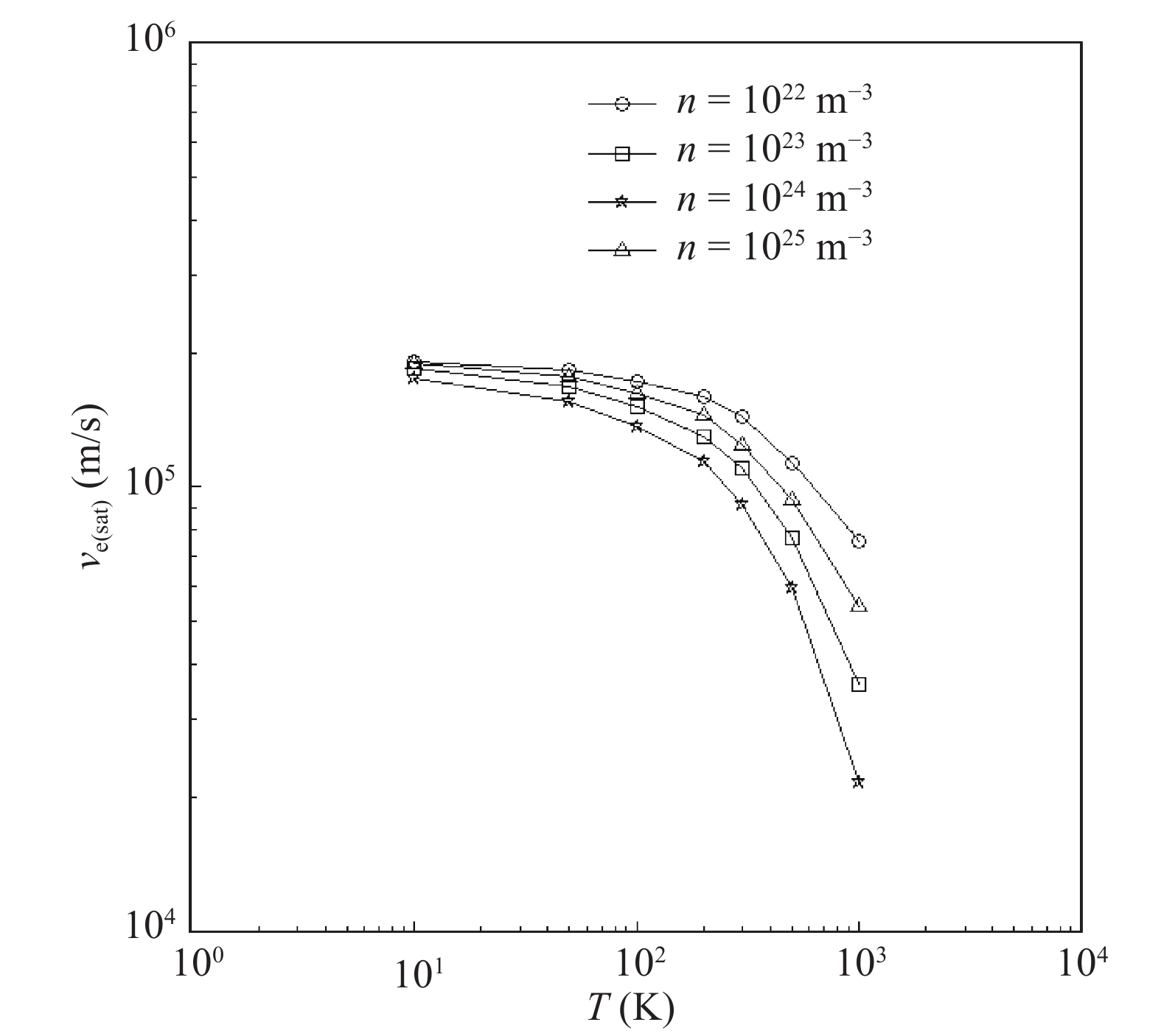
Abstract: The hot electron transport in wurtzite phase gallium nitride (Wz-GaN) has been studied in this paper. An analytical expression of electron drift velocity under the condition of impact ionization has been developed by considering all major scattering mechanisms such as deformation potential acoustic phonon scattering, piezoelectric acoustic phonon scattering, optical phonon scattering, electron-electron scattering and ionizing scattering. Numerical calculations show that electron drift velocity in Wz-GaN saturates at 1.44 × 10⁵ m/s at room temperature for the electron concentration of 1022 m−3. The effects of temperature and doping concentration on the hot electron drift velocity in Wz-GaN have also been studied. Results show that the saturation electron drift velocity varies from 1.91 × 10⁵–0.77 × 10⁵ m/s for the change in temperature within the range of 10–1000 K, for the electron concentration of 1022 m−3; whereas the same varies from 1.44 × 10⁵–0.91 × 10⁵ m/s at 300 K for the variation in the electron concentration within the range of 1022–1025 m−3. The numerically calculated results have been compared with the Monte Carlo simulated results and experimental data reported earlier, and those are found to be in good agreement.

Key words: electron drift velocityhot electron transportGaNscattering limited velocity


[1]
Kolnik J, Oguzman I H, Brennan K F, et al. Electronic transport studies of bulk zincblende and wurtzite phases of GaN based on an ensemble Monte Carlo calculation including a full zone band structure. J Appl Phys, 1995, 78(2): 1033 doi: 10.1063/1.360405
[2]
Bhapkar U V, Shur M S. Monte Carlo calculation of velocity-field characteristics of wurtzite GaN. J Appl Phys, 1997, 82(4): 1649 doi: 10.1063/1.365963
[3]
Binesh A R, Arabshahi H, Ebrahimi G R, et al. Temperature dependence of high field electron transport properties in wurtzite phase GaN for device modelling. Int J Mod Phys B, 2008, 22(22): 3915 doi: 10.1142/S0217979208048620
[4]
Khan M A, Chen Q, Sure M S, et al. GaN based heterostructure for high power devices. Solid-State Electron, 1999, 41: 1555
[5]
Wraback M, Shen H, Carrano J C, et al. Time-resolved electroabsorption measurement of the electron velocity-field characteristic in GaN. Appl Phys Lett, 2000, 76: 1155 doi: 10.1063/1.125968
[6]
Barker J M, Akis R, Ferry D K, et al. High-field transport studies of GaN. Physica B, 2002, 314: 39 doi: 10.1016/S0921-4526(01)01453-3
[7]
Acharyya A, Banerjee J P. Prospects of IMPATT devices based on wide bandgap semiconductors as potential terahertz sources. Appl Nanosci, 2014, 4: 1 doi: 10.1007/s13204-012-0172-y
[8]
Ghosh M, Mondal M, Acharyya A. The effect of electron versus hole photocurrent on opto-electric properties of p+–p–n–n+ Wz-GaN reach-through avalanche photodiodes. Adv Optoelectron, 2013, 2013: 840931 doi: 10.1155/2013/840931
[9]
Nakamura S, Mukai T, Senoh M. Candela-class high-brightness InGaN/AlGaN double-heterostructure blue-light-emitting diodes. Appl Phys Lett, 1994, 64: 1687 doi: 10.1063/1.111832
[10]
Pengelly R S, Wood S M, Milligan J W, et al. A review of GaN on SiC high electron-mobility power transistors and MMICs. IEEE Trans Microwave Theory Tech, 2012, 60(6): 1764 doi: 10.1109/TMTT.2012.2187535
[11]
Acharyya A, Banerjee J P. Potentiality of IMPATT devices as terahertz source: an avalanche response time based approach to determine the upper cut-off frequency limits. IETE J Res, 2013, 59(2): 118 doi: 10.4103/0377-2063.113029
[12]
Acharyya A, Banerjee J P. Prospects of IMPATT devices based on wide bandgap semiconductors as potential terahertz sources. Appl Nanosci, 2014, 4: 1 doi: 10.1007/s13204-012-0172-y
[13]
Bandyopadhyay A M, Acharyya A, Banerjee J P. Multiple-band large-signal characterization of millimeter-wave double avalanche region transit time diode. J Comput Electron, 2014, 13: 769 doi: 10.1007/s10825-014-0599-3
[14]
Acharyya A, Banerjee S, Banerjee J P. Effect of junction temperature on the large-signal properties of a 94 GHz silicon based double-drift region impact avalanche transit time device. J Semicond, 2013, 34(2): 024001 doi: 10.1088/1674-4926/34/2/024001
[15]
Acharyya A, Goswami J, Banerjee, S, et al. Quantum corrected drift-diffusion model for terahertz IMPATTs based on different semiconductors. J Comput Electron, 2015, 14: 309 doi: 10.1007/s10825-014-0658-9
[16]
Acharyya A, Banerjee J P. Design and simulation of silicon carbide poly-type double-drift region avalanche photodiodes for UV sensing. J Optoelectron Adv Mater, 2012, 14(7/8): 630
[17]
Ghosh M, Mondal M, Acharyya A. The effect of electron versus hole photocurrent on opto-electric properties of p+–p–n–n+ Wz-GaN reach-through avalanche photodiodes. Adv Optoelectron, 2013, 2013: 1
[18]
Acharyya A, Ghosh S. Dark current reduction in nano-avalanche photodiodes by incorporating multiple quantum barriers. Int J Electron, 2017, 104(12): 1957 doi: 10.1080/00207217.2017.1330426
[19]
Acharyya A, Banerjee J P. A generalized analytical model based on multistage scattering phenomena for estimating the impact ionization rate of charge carriers in semiconductors. J Comput Electron, 2014, 13: 917 doi: 10.1007/s10825-014-0608-6
[20]
Acharyya A. Diminution of impact ionization rate of charge carriers in semiconductors due to acoustic phonon scattering. Appl Phys A, 2017, 123: 629 doi: 10.1007/s00339-017-1245-2
[21]
Mall J L. Physics of semiconductors. New York: McGraw Hill, 1964: 208
[22]
Electronic Archive: New Semiconductor Materials, Characteristics and Properties. http://www.ioffe.rssi.ru/SVA/NSM/Semicond/GaN/index.html. (2017). Accessed 3 October 2017
[23]
Bougrov V, Levinshtein M E, Rumyantsev S L, et al. Properties of advanced semiconductor materials GaN, AlN, InN, BN, SiC, SiGe. New York: John Wiley & Sons, Inc, 2001
[24]
Suzuki M, Uenoyama T, Yanase A. First-principles calculations of effective-mass parameters of AlN and GaN. Phys Rev B, 1995, 52: 8132 doi: 10.1103/PhysRevB.52.8132
[25]
Chin V W L, Tansley T L, Osotchan T. Electron mobilities in gallium, indium, and aluminum nitrides. J Appl Phys, 1994, 75(11): 7365 doi: 10.1063/1.356650
[26]
Acharyya A, Chatterjee S, Das A, et al. Additional confirmation of a generalized analytical model based on multistage scattering phenomena to evaluate the ionization rates of charge carriers in semiconductors. J Comput Electron, 2016, 15: 34 doi: 10.1007/s10825-015-0746-5
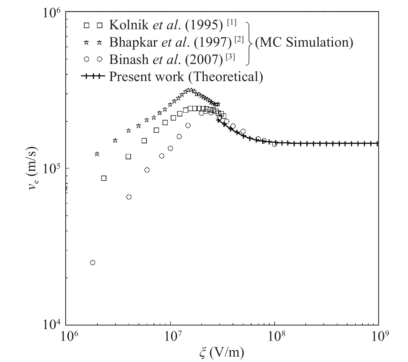
Fig. 1.  Variations of electron drift velocity in Wz-GaN with electric field at 300 K for the electron concentration of 1022 m−3 obtained from the MC simulations carried out by other researchers[13] as well as from the analytical expression developed in this paper.

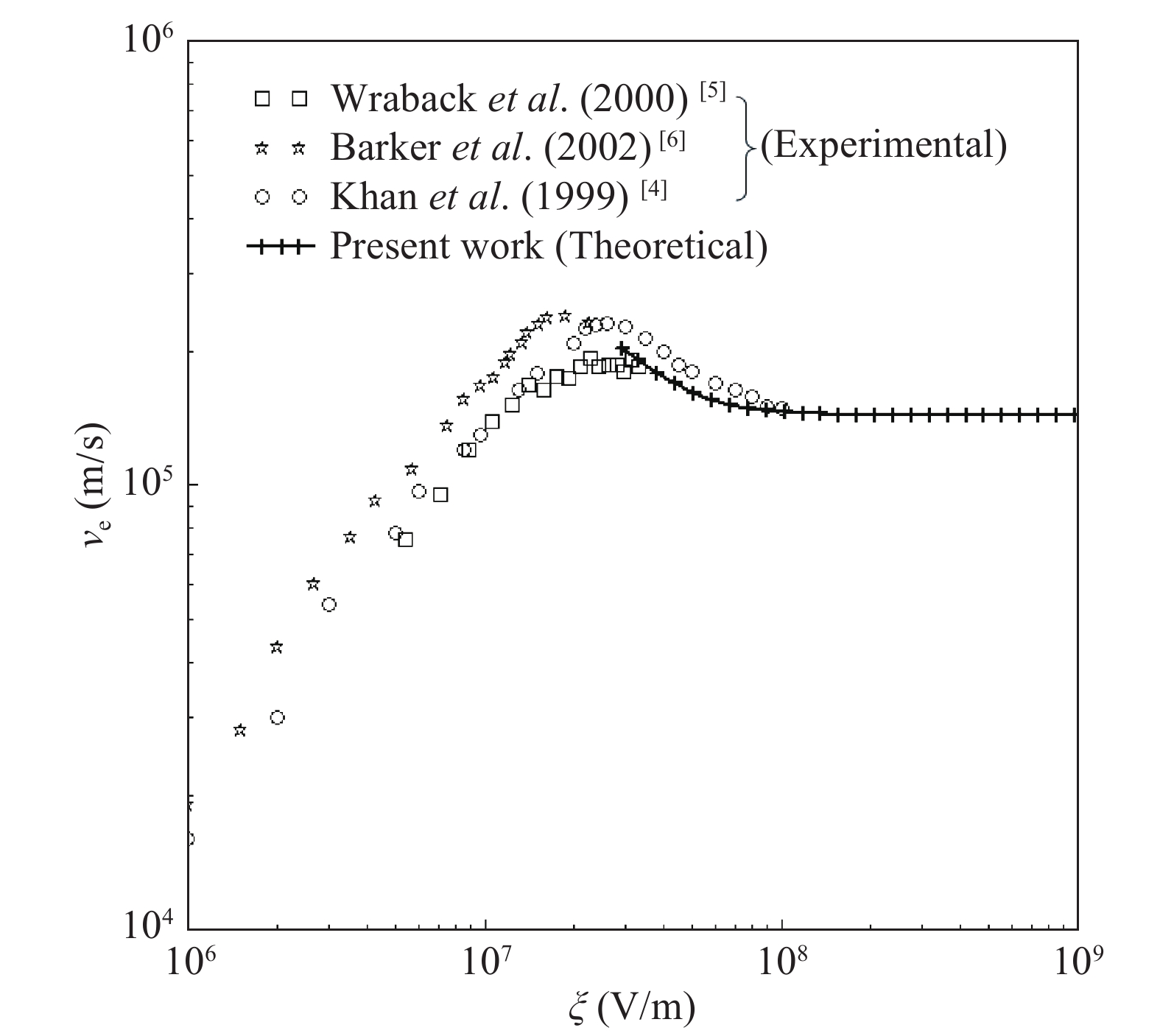
Fig. 2.  Variations of electron drift velocity in Wz-GaN with electric field at 300 K for the electron concentration of 1022 m−3 obtained from the experimental measurements carried out by other researchers[46] as well as from the analytical expression developed in this paper.

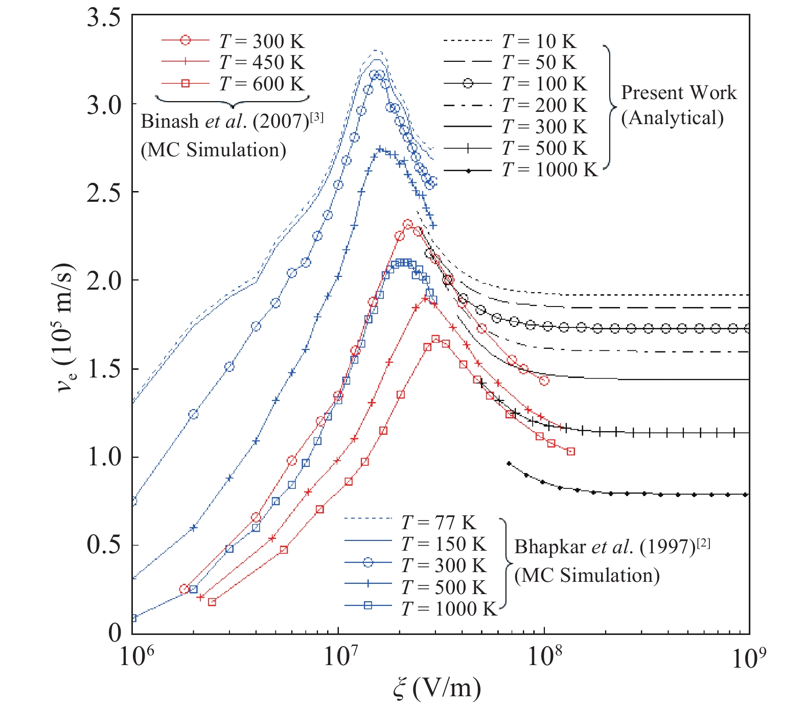
Fig. 3.  (Color online) Variations of electron drift velocity in Wz-GaN with electric field at different temperatures for the electron concentration of 1022 m−3 obtained from the MC simulations carried out by other researchers[2, 3] as well as from the analytical expression developed in this paper.

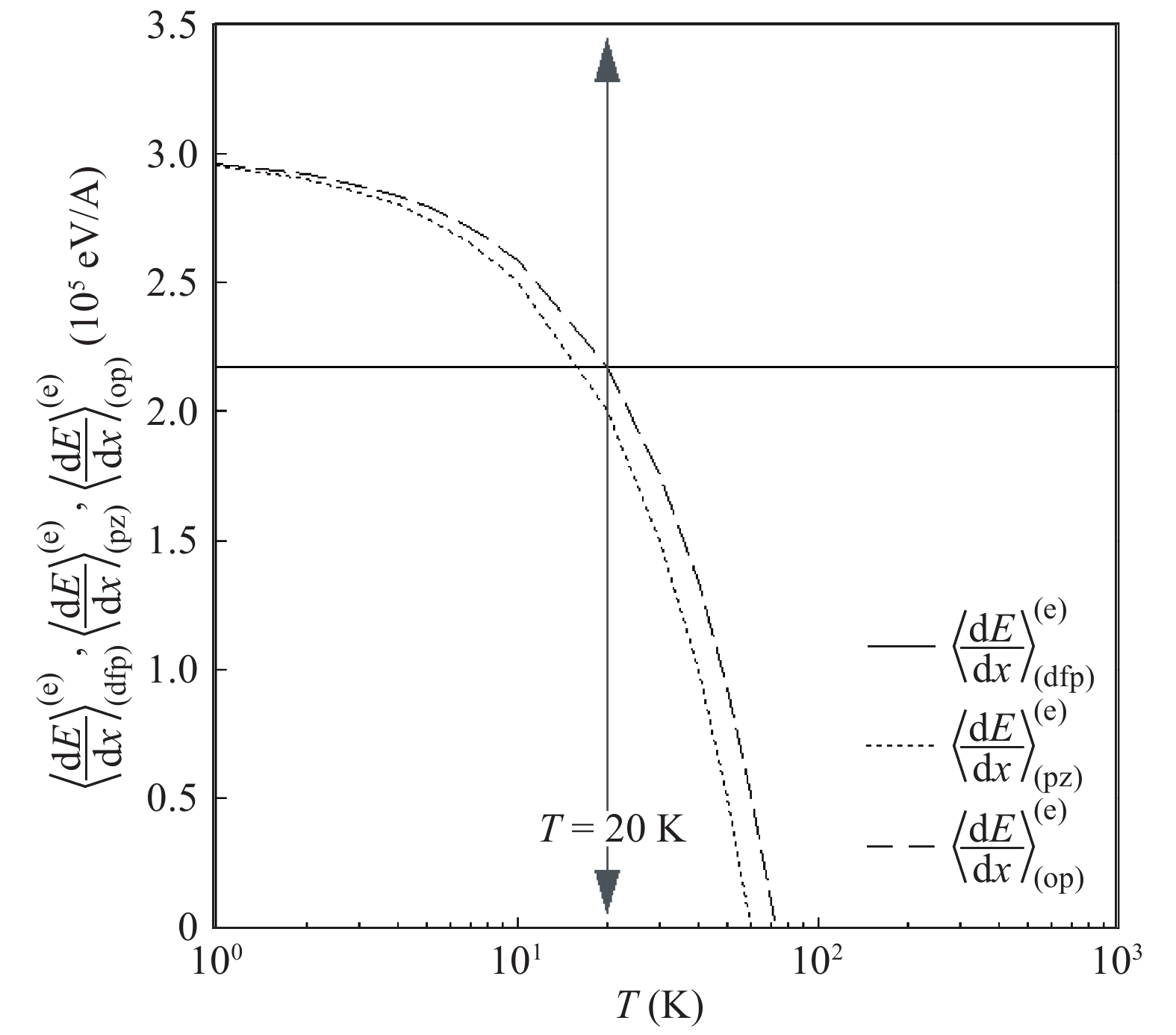
Fig. 4.  Variations of average energy loss per unit length by an electron due to deformation potential acoustic phonon scattering, piezoelectric acoustic phonon scattering and optical phonon scattering with temperature.

Fig. 5.  Variations of electron saturation drift velocity in Wz-GaN with temperature for different electron concentrations at the applied electric field of 5.0 × 10⁸ V/m obtained from the analytical expression developed in this paper.

Table 1.   Values of important parameters of Wz-GaN at 300 K[2226].

Type of parameter Parameter Value
Material parameter εr 8.91
$m_{\rm {e}}^*$ (Kg) (m0 = 9.1×10⁻³¹ Kg) 0.20m0
${E_{\rm g}}$ (eV) 3.39
$E_{\left( {\rm {dfp}} \right)}^{\left({\rm {e}} \right)}$ (meV) 18.41
$l_{\left( {\rm {dfp}} \right)}^{\left({\rm {e}} \right)}$ (Å) 30.90
$E_{\left( {\rm {pz}} \right)}^{\left({\rm {e}} \right)}$ (meV) 15.10
$l_{\left( {\rm {pz}} \right)}^{\left({\rm {e}} \right)}$ (Å) 22.50
$E_{\left( {\rm {op}} \right)}^{\left({\rm {e}} \right)}$ (meV) 91.20
$l_{\left( {\rm {op}} \right)}^{\left({\rm {e}} \right)}$ (Å) 42.00
$E_{\left( {\rm {i}} \right)}^{\left({\rm {e}} \right)}$ (eV) 3.66
$l_{\left( {\rm {i}} \right)}^{\left({\rm {e}} \right)}$ (Å) 840.00
Dimensionless fitting parameters for calculating $l_{\left( {\rm {ee}} \right)}^{\left({\rm {e}} \right)}$ as a function of electron density G 0.75
c 3.12
DownLoad: CSV
[1]
Kolnik J, Oguzman I H, Brennan K F, et al. Electronic transport studies of bulk zincblende and wurtzite phases of GaN based on an ensemble Monte Carlo calculation including a full zone band structure. J Appl Phys, 1995, 78(2): 1033 doi: 10.1063/1.360405
[2]
Bhapkar U V, Shur M S. Monte Carlo calculation of velocity-field characteristics of wurtzite GaN. J Appl Phys, 1997, 82(4): 1649 doi: 10.1063/1.365963
[3]
Binesh A R, Arabshahi H, Ebrahimi G R, et al. Temperature dependence of high field electron transport properties in wurtzite phase GaN for device modelling. Int J Mod Phys B, 2008, 22(22): 3915 doi: 10.1142/S0217979208048620
[4]
Khan M A, Chen Q, Sure M S, et al. GaN based heterostructure for high power devices. Solid-State Electron, 1999, 41: 1555
[5]
Wraback M, Shen H, Carrano J C, et al. Time-resolved electroabsorption measurement of the electron velocity-field characteristic in GaN. Appl Phys Lett, 2000, 76: 1155 doi: 10.1063/1.125968
[6]
Barker J M, Akis R, Ferry D K, et al. High-field transport studies of GaN. Physica B, 2002, 314: 39 doi: 10.1016/S0921-4526(01)01453-3
[7]
Acharyya A, Banerjee J P. Prospects of IMPATT devices based on wide bandgap semiconductors as potential terahertz sources. Appl Nanosci, 2014, 4: 1 doi: 10.1007/s13204-012-0172-y
[8]
Ghosh M, Mondal M, Acharyya A. The effect of electron versus hole photocurrent on opto-electric properties of p+–p–n–n+ Wz-GaN reach-through avalanche photodiodes. Adv Optoelectron, 2013, 2013: 840931 doi: 10.1155/2013/840931
[9]
Nakamura S, Mukai T, Senoh M. Candela-class high-brightness InGaN/AlGaN double-heterostructure blue-light-emitting diodes. Appl Phys Lett, 1994, 64: 1687 doi: 10.1063/1.111832
[10]
Pengelly R S, Wood S M, Milligan J W, et al. A review of GaN on SiC high electron-mobility power transistors and MMICs. IEEE Trans Microwave Theory Tech, 2012, 60(6): 1764 doi: 10.1109/TMTT.2012.2187535
[11]
Acharyya A, Banerjee J P. Potentiality of IMPATT devices as terahertz source: an avalanche response time based approach to determine the upper cut-off frequency limits. IETE J Res, 2013, 59(2): 118 doi: 10.4103/0377-2063.113029
[12]
Acharyya A, Banerjee J P. Prospects of IMPATT devices based on wide bandgap semiconductors as potential terahertz sources. Appl Nanosci, 2014, 4: 1 doi: 10.1007/s13204-012-0172-y
[13]
Bandyopadhyay A M, Acharyya A, Banerjee J P. Multiple-band large-signal characterization of millimeter-wave double avalanche region transit time diode. J Comput Electron, 2014, 13: 769 doi: 10.1007/s10825-014-0599-3
[14]
Acharyya A, Banerjee S, Banerjee J P. Effect of junction temperature on the large-signal properties of a 94 GHz silicon based double-drift region impact avalanche transit time device. J Semicond, 2013, 34(2): 024001 doi: 10.1088/1674-4926/34/2/024001
[15]
Acharyya A, Goswami J, Banerjee, S, et al. Quantum corrected drift-diffusion model for terahertz IMPATTs based on different semiconductors. J Comput Electron, 2015, 14: 309 doi: 10.1007/s10825-014-0658-9
[16]
Acharyya A, Banerjee J P. Design and simulation of silicon carbide poly-type double-drift region avalanche photodiodes for UV sensing. J Optoelectron Adv Mater, 2012, 14(7/8): 630
[17]
Ghosh M, Mondal M, Acharyya A. The effect of electron versus hole photocurrent on opto-electric properties of p+–p–n–n+ Wz-GaN reach-through avalanche photodiodes. Adv Optoelectron, 2013, 2013: 1
[18]
Acharyya A, Ghosh S. Dark current reduction in nano-avalanche photodiodes by incorporating multiple quantum barriers. Int J Electron, 2017, 104(12): 1957 doi: 10.1080/00207217.2017.1330426
[19]
Acharyya A, Banerjee J P. A generalized analytical model based on multistage scattering phenomena for estimating the impact ionization rate of charge carriers in semiconductors. J Comput Electron, 2014, 13: 917 doi: 10.1007/s10825-014-0608-6
[20]
Acharyya A. Diminution of impact ionization rate of charge carriers in semiconductors due to acoustic phonon scattering. Appl Phys A, 2017, 123: 629 doi: 10.1007/s00339-017-1245-2
[21]
Mall J L. Physics of semiconductors. New York: McGraw Hill, 1964: 208
[22]
Electronic Archive: New Semiconductor Materials, Characteristics and Properties. http://www.ioffe.rssi.ru/SVA/NSM/Semicond/GaN/index.html. (2017). Accessed 3 October 2017
[23]
Bougrov V, Levinshtein M E, Rumyantsev S L, et al. Properties of advanced semiconductor materials GaN, AlN, InN, BN, SiC, SiGe. New York: John Wiley & Sons, Inc, 2001
[24]
Suzuki M, Uenoyama T, Yanase A. First-principles calculations of effective-mass parameters of AlN and GaN. Phys Rev B, 1995, 52: 8132 doi: 10.1103/PhysRevB.52.8132
[25]
Chin V W L, Tansley T L, Osotchan T. Electron mobilities in gallium, indium, and aluminum nitrides. J Appl Phys, 1994, 75(11): 7365 doi: 10.1063/1.356650
[26]
Acharyya A, Chatterjee S, Das A, et al. Additional confirmation of a generalized analytical model based on multistage scattering phenomena to evaluate the ionization rates of charge carriers in semiconductors. J Comput Electron, 2016, 15: 34 doi: 10.1007/s10825-015-0746-5
  • Search

    Advanced Search >>

    GET CITATION

    shu

    Export: BibTex EndNote

    Article Metrics

    Article views: 3932 Times PDF downloads: 57 Times Cited by: 0 Times

    History

    Received: 01 November 2017 Revised: 11 January 2018 Online: Accepted Manuscript: 04 April 2018Uncorrected proof: 12 April 2018Published: 01 July 2018

    Catalog

      Email This Article

      User name:
      Email:*请输入正确邮箱
      Code:*验证码错误
      Aritra Acharyya. Hot electron transport in wurtzite-GaN: effects of temperature and doping concentration[J]. Journal of Semiconductors, 2018, 39(7): 072002. doi: 10.1088/1674-4926/39/7/072002 ****A Acharyya, Hot electron transport in wurtzite-GaN: effects of temperature and doping concentration[J]. J. Semicond., 2018, 39(7): 072002. doi: 10.1088/1674-4926/39/7/072002.
      Citation:
      Aritra Acharyya. Hot electron transport in wurtzite-GaN: effects of temperature and doping concentration[J]. Journal of Semiconductors, 2018, 39(7): 072002. doi: 10.1088/1674-4926/39/7/072002 ****
      A Acharyya, Hot electron transport in wurtzite-GaN: effects of temperature and doping concentration[J]. J. Semicond., 2018, 39(7): 072002. doi: 10.1088/1674-4926/39/7/072002.

      Hot electron transport in wurtzite-GaN: effects of temperature and doping concentration

      DOI: 10.1088/1674-4926/39/7/072002
      More Information
      • Corresponding author: ari_besu@yahoo.co.in
      • Received Date: 2017-11-01
      • Revised Date: 2018-01-11
      • Published Date: 2018-07-01

      Catalog

        /

        DownLoad:  Full-Size Img  PowerPoint
        Return
        Return