J. Semicond. > 2018, Volume 39 > Issue 7 > 073001

SEMICONDUCTOR MATERIALS

Controlling morphology evolution of AlN nanostructures: influence of growth conditions in physical vapor transport

Lei Jin, Hongjuan Cheng, Jianli Chen, Song Zhang, Yongkuan Xu and Zhanping Lai

+ Author Affiliations

 Corresponding author: Lei Jin, jinlei851024@126.com

DOI: 10.1088/1674-4926/39/7/073001

PDF

Turn off MathJax

Abstract: A series of AlN nanostructures were synthesized by an ultrahigh-temperature, catalyst-free, physical vapor transport (PVT) process. Energy dispersive X-ray spectroscopy (EDX), X-ray diffraction (XRD), X-Ray photoelectron spectroscopy (XPS), high resolution transmission electron microscopy (HRTEM) detection show that high quality AlN nanowires were prepared. Nanostructures including nanorings, nanosprings, nanohelices, chain-like nanowires, six-fold symmetric nanostructure and rod-like structure were successfully obtained by controlling the growth duration and temperature. The morphology evolution was attributed to electrostatic polar charge model and the crystalline lattice structure of AlN.

Key words: AlN nanowireultrahigh-temperaturecatalyst-freePVTmorphology evolution


[1]
Zhou C J, Yang Y, Shu Y, et al. Visible-light photoresponse of AlN-based film bulk acoustic wave resonator. Appl Phys Lett, 2013, 102: 191914 doi: 10.1063/1.4807135
[2]
Sorokin B P, Kvashnin G M, Volkov A P, et al. AlN/single crystalline diamond piezoelectric structure as a high overtone bulk acoustic resonator. Appl Phys Lett, 2013, 102: 113507 doi: 10.1063/1.4798333
[3]
Liu G, Zhou G G, Qin Z Y, et al. Luminescence characterizations of freestanding bulk single crystalline aluminum nitride towards optoelectronic application. Crystengcomm, 2017, 19(37): 5522 doi: 10.1039/C7CE01239J
[4]
He J H, Yang R S, Chueh Y L, et al. Aligned AlN nanorods with multi-tipped surfaces-growth, field-emission, and cathodoluminescence properties. Adv Mater, 2006, 18: 650 doi: 10.1002/(ISSN)1521-4095
[5]
Sheppard L M. Aluminum nitride: a versatile but challenging material. Am Ceram Soc Bull, 1990, 69: 1801
[6]
Yang J, Liu T W, Hsu C W, et al. Controlled growth of aluminium nitride nanorod arrays via chemical vapour deposition. Nanotechnology, 2006, 17: S321 doi: 10.1088/0957-4484/17/11/S15
[7]
Li J J, Song B, Wu R, et al. Preparation and optical properties of free-standing transparent aluminum nitride film assembled by aligned nanorods. J Am Ceram Soc, 2012, 95: 870
[8]
Zheng J, Yang Y, Yu B, et al. [0001] oriented aluminum nitride one-dimensional nanostructures: synthesis, structure evolution, and electrical properties. ACS Nano, 2007, 2: 134
[9]
Tondare V N, Balasubramanian C, Shende S V, et al. Field emission from open ended aluminum nitride nanotubes. Appl Phys Lett, 2002, 80: 4813 doi: 10.1063/1.1482137
[10]
Lei W W, Liu D, Zhu P W, et al. One-step synthesis of AlN branched nanostructures by an improved DC arc discharge plasma method. CrystEngComm, 2010, 12: 511 doi: 10.1039/B910735E
[11]
Lei M, Yang H, Guo Y F, et al. Synthesis and optical property of high purity AlN nanowires. Mater Sci Eng B, 2007, 143: 85 doi: 10.1016/j.mseb.2007.07.068
[12]
Liu F, Su Z J, Mo F Y, et al. Controlled synthesis of ultra-long AlN nanowires in different densities and in situ investigation of the physical properties of an individual AlN nanowire. Nanoscale, 2011, 3: 610 doi: 10.1039/C0NR00586J
[13]
Meng F, Estruga M, Forticaux A, et al. Formation of stacking faults and the screw dislocation-driven growth: a case study of aluminum nitride nanowires. ACS Nano, 2013, 7: 11369 doi: 10.1021/nn4052293
[14]
Iwata M, Adachi K, Furukawa S, et al. Synthesis of purified AlN nano powder by transferred type arc plasma. J Phys D, 2004, 37: 1041 doi: 10.1088/0022-3727/37/7/014
[15]
Duan J H, Yang S G, Liu H W, et al. AlN nanorings. J Cryst Growth, 2005, 283: 291 doi: 10.1016/j.jcrysgro.2005.06.015
[16]
Wang H, Liu G, Yang W, et al. Bicrystal AlN zigzag nanowires. J Phys Chem C, 2007, 111: 17169 doi: 10.1021/jp077435u
[17]
Cimalla V, Foerster C, Cengher D, et al. Growth of AlN nanowires by metal organic chemical vapour deposition. Phys Status Solid B, 2006, 243: 1476 doi: 10.1002/(ISSN)1521-3951
[18]
Zhang X H, Shao R W, Jin L, et al. Helical growth of aluminum nitride: new insights into its growth habit from nanostructures to single crystals. Sci Rep, 2015, 5: 10087 doi: 10.1038/srep10087
[19]
Epelbaum B M, Seitz C, Magerl A, et al. Natural growth habit of bulk AlN crystals. J Cryst Growth, 2004, 265: 577 doi: 10.1016/j.jcrysgro.2004.02.100
[20]
Liu Y, Jiang L B, Wang G, et al. Adjustable nitrogen-vacancy induced magnetism in AlN. Appl Phys Lett, 2012, 100: 122401 doi: 10.1063/1.3696023
[21]
Lei M, Song B, Guo X, et al. Large-scale AlN nanowires synthesized by direct sublimation method. J Eur Ceram Soc, 2009, 29: 195-200 doi: 10.1016/j.jeurceramsoc.2008.06.002
[22]
Kong X Y, Wang Z L. Spontaneous polarization-induced nanohelixes, nanosprings, and nanorings of piezoelectric nanobelts. Nano Lett, 2003, 3: 1625 doi: 10.1021/nl034463p
[23]
Yang R, Ding Y, Wang Z L, et al. Deformation-free single-crystal nanohelixes of polar nanowires. Nano Lett, 2004, 4: 1309 doi: 10.1021/nl049317d
[24]
Wang X Q, Xi G C, Xiong S L, et al. Solution-phase synthesis of single-crystal CuO nanoribbons and nanorings. Cryst Growth Des, 2007, 7: 930 doi: 10.1021/cg060798j
[25]
Jian J K, Zhang Z H, Sun Y P. GaN nanorings: another example of spontaneous polarization-induced nanostructure. J Cryst Growth, 2007, 303: 427 doi: 10.1016/j.jcrysgro.2006.11.209
[26]
Kuang X P, Zhang H Y, Wang G G, et al. Effect of deposition temperature on the microstructure and surface morphology of c-axis oriented AlN films deposited on sapphire substrate by RF reactive magnetron sputtering. Superlattice Microstruct, 2012, 52: 931 doi: 10.1016/j.spmi.2012.08.003
[27]
Ishihara M, Li S J, Yumoto H, et al. Control of preferential orientation of AlN films prepared by the reactive sputtering method. Thin Solid Films, 1998, 316: 152 doi: 10.1016/S0040-6090(98)00406-4
[28]
Xu X H, Wu H S, Zhang C J, et al. Morphological properties of AlN piezoelectric thin films deposited by DC reactive magnetron sputtering. Thin Solid Films, 2001, 388: 62 doi: 10.1016/S0040-6090(00)01914-3
[29]
Bickermann M, Epelbaum B M, Filip O, et al. Growth of AlN bulk crystals on SiC seeds: chemical analysis and crystal properties. Phys Status Solidi C, 2012, 9: 449 doi: 10.1002/pssc.v9.3/4
[30]
Noveski V, Schlesser R, Raghothamachar B, et al. Seeded growth of bulk AlN crystals and grain evolution in polycrystalline AlN boules. J Cryst Growth, 2005, 279: 13 doi: 10.1016/j.jcrysgro.2004.12.027
[31]
Hartmann C, Wollweber J, Dittmar A, et al. Preparation of bulk AlN seeds by spontaneous nucleation of freestanding crystals. Jpn J Appl Phys, 2013, 52: 08JA06 doi: 10.7567/JJAP.52.08JA06
Fig. 1.  (Color online) (a) Schematic diagram of growth typical PVT sublimation configuration. (b) Photograph of the products. (c) SEM image with EDX spectrum displayed in the inset.

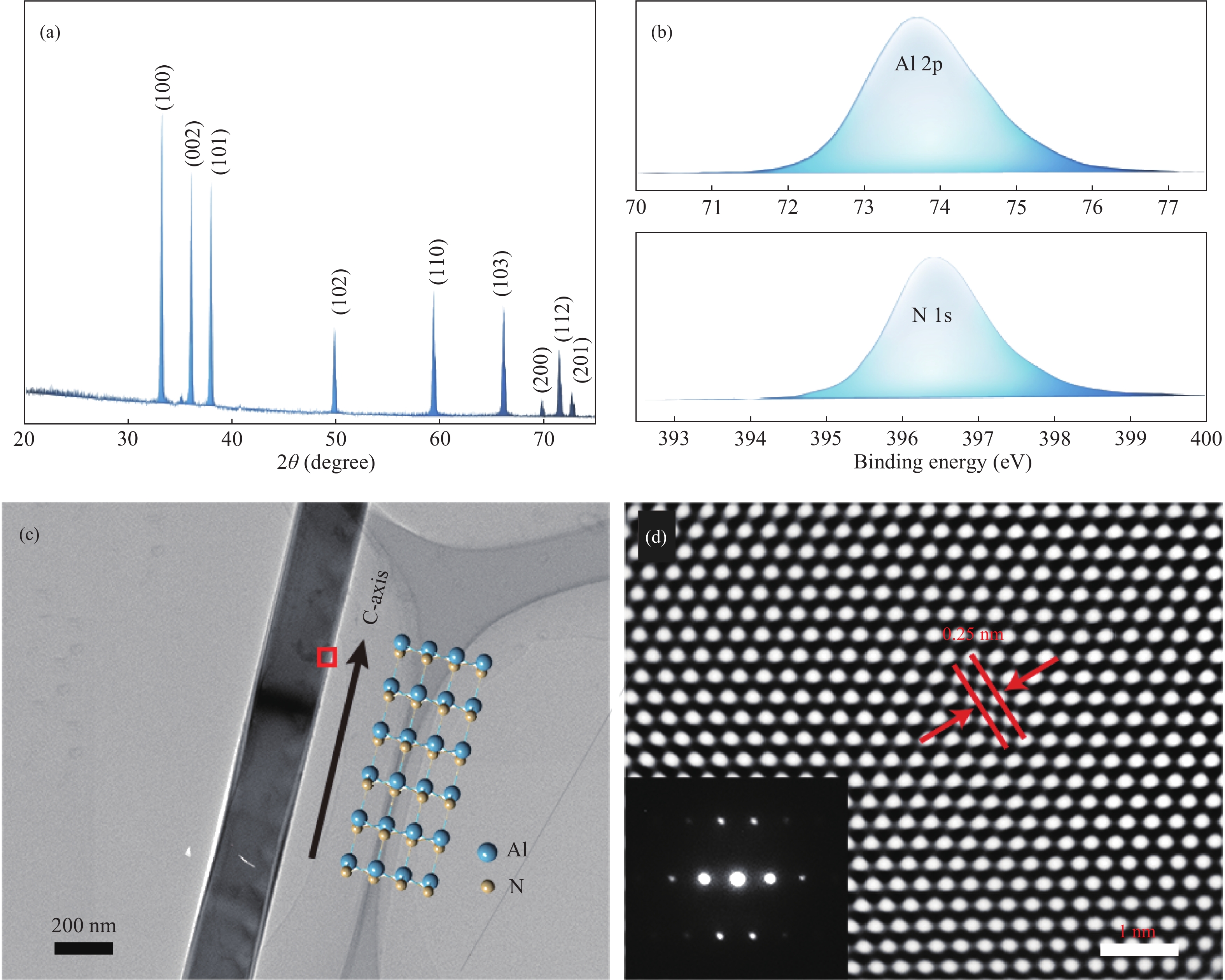
Fig. 2.  (Color online) (a) XRD spectra of as-grown product. (b) XPS spectra of the AlN nanowires, upper shows Al 2p spectrum and N 1s spectrum is displayed below. (c) TEM image of a single AlN nanowire. (d) HRTEM image for the dot as denoted by the red box in (c). The inset in (d) shows the SAED pattern.

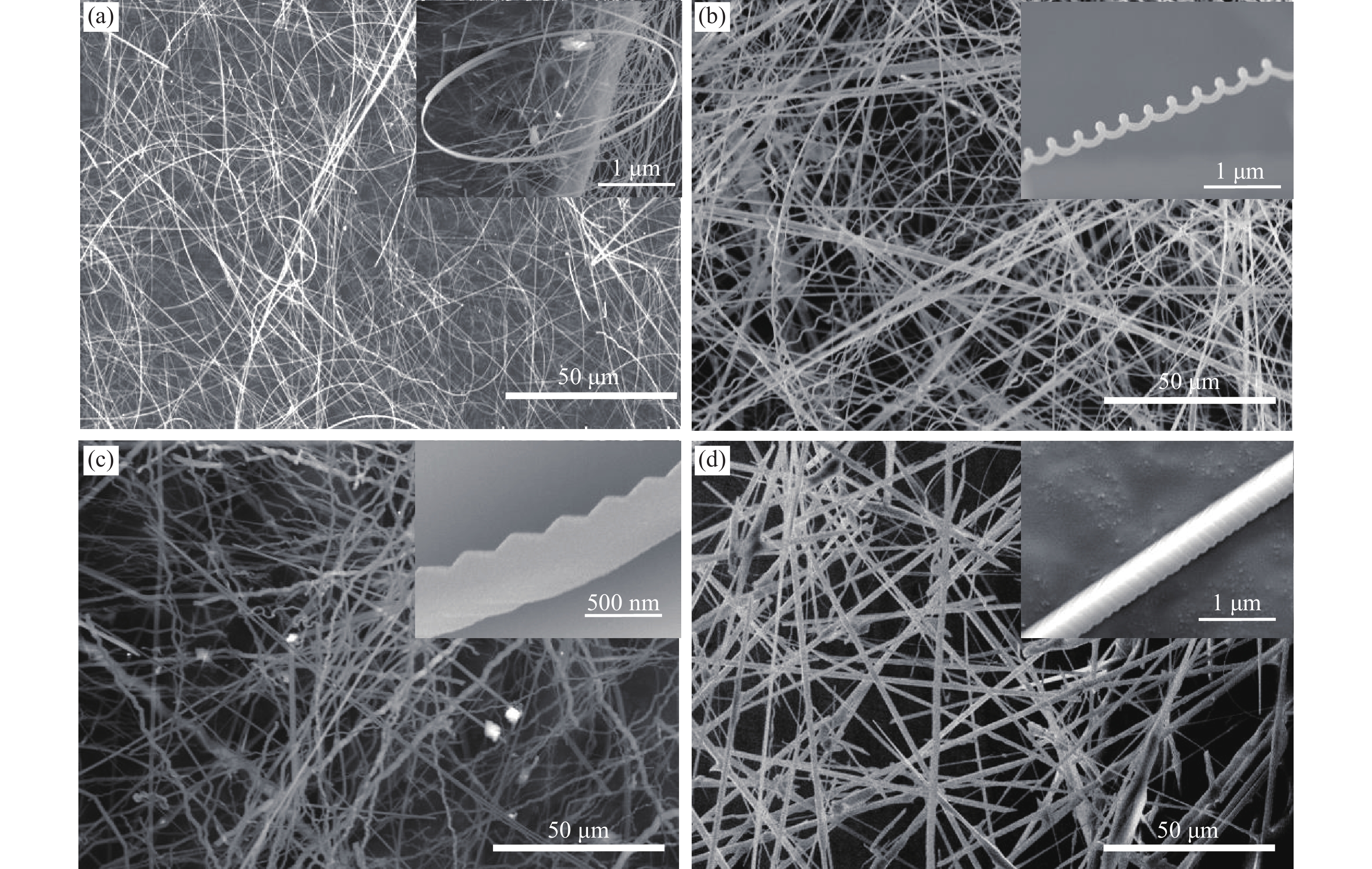
Fig. 3.  SEM images of AlN nanostructure with different growth duration at 1800 °C. (a) 20 min. (b) 40 min. (c) 80 min. (d) 180 min. The details morphology of individual AlN nanostructure corresponding to (a)–(d) are shown in the inset each image, respectively.

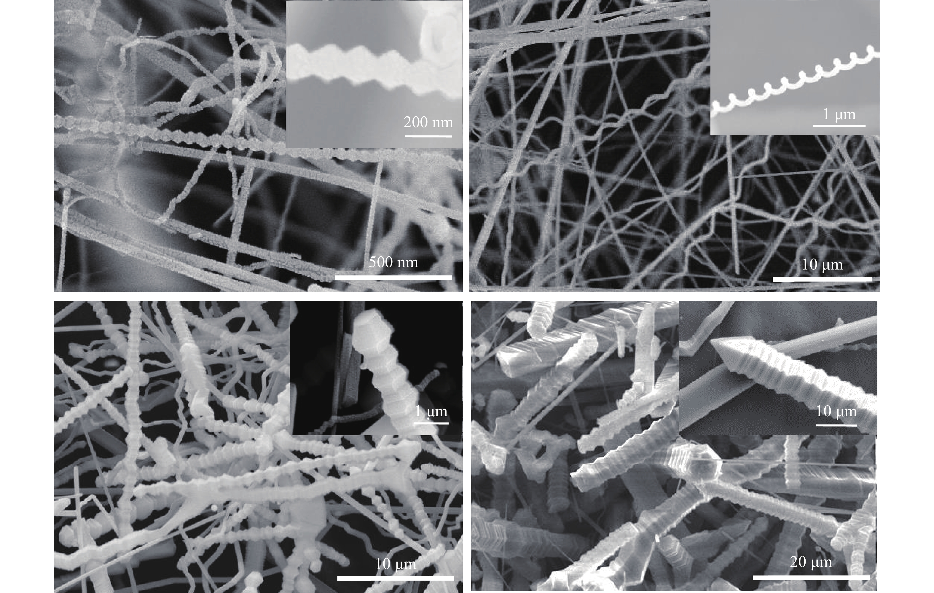
Fig. 4.  SEM images of AlN nanostructure with different growth temperature in 40 min growth duration. (a) 1750 °C. (b) 1800 °C. (c) 1850 °C. (d) 1900 °C. The details morphology of individual AlN nanostructure corresponding to (a)–(d) are shown in the inset each image, respectively.

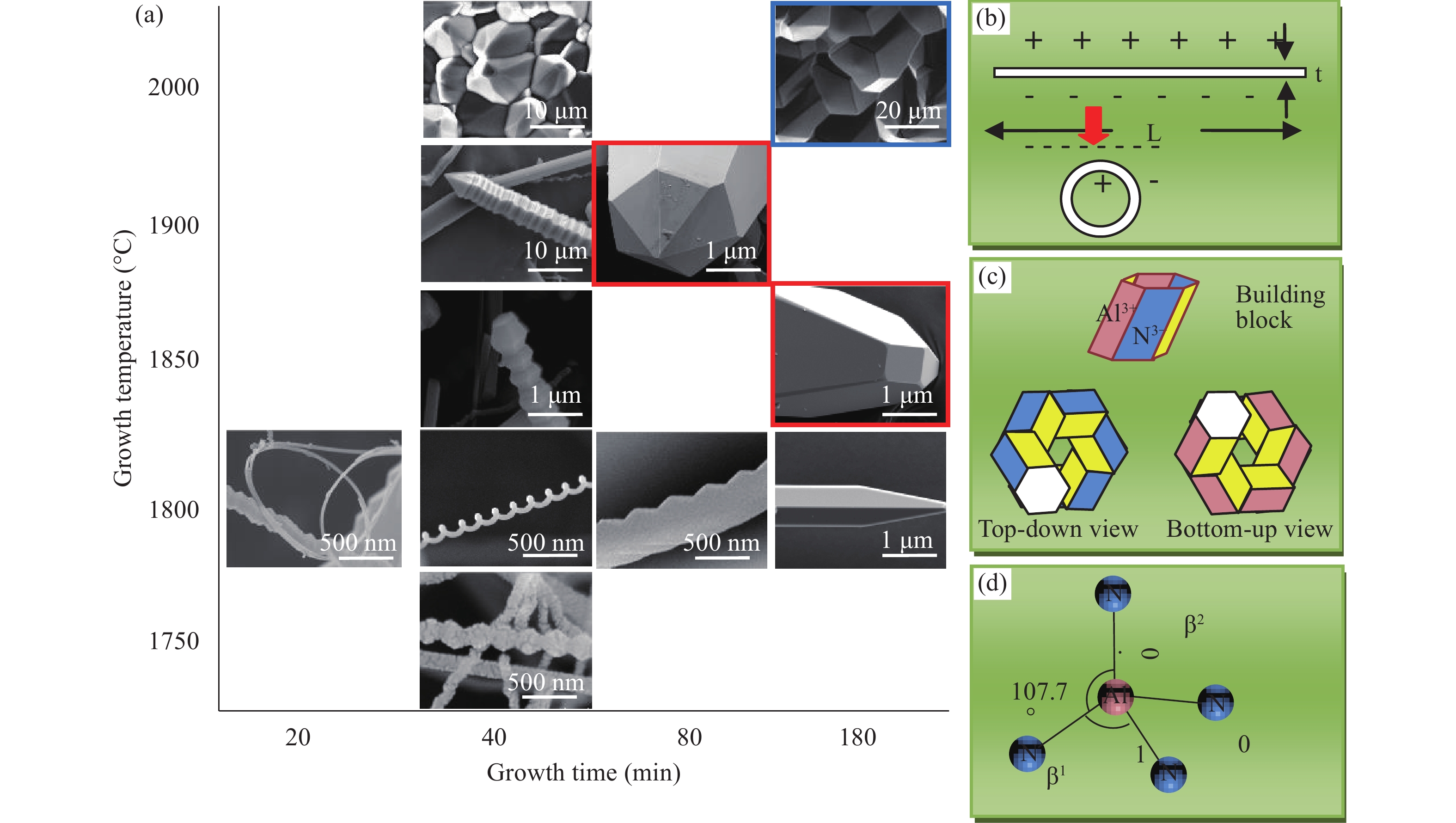
Fig. 5.  (Color online) (a) The morphological dependence of AlN nanostructures on the heating temperature and growth time. (b) A schematic model of a nanowire as viewed parallel to its flat surfaces. (c) The bottom-up and top-down views of the nanohelical model. (d) Atomic structure of wurtzite AlN.

[1]
Zhou C J, Yang Y, Shu Y, et al. Visible-light photoresponse of AlN-based film bulk acoustic wave resonator. Appl Phys Lett, 2013, 102: 191914 doi: 10.1063/1.4807135
[2]
Sorokin B P, Kvashnin G M, Volkov A P, et al. AlN/single crystalline diamond piezoelectric structure as a high overtone bulk acoustic resonator. Appl Phys Lett, 2013, 102: 113507 doi: 10.1063/1.4798333
[3]
Liu G, Zhou G G, Qin Z Y, et al. Luminescence characterizations of freestanding bulk single crystalline aluminum nitride towards optoelectronic application. Crystengcomm, 2017, 19(37): 5522 doi: 10.1039/C7CE01239J
[4]
He J H, Yang R S, Chueh Y L, et al. Aligned AlN nanorods with multi-tipped surfaces-growth, field-emission, and cathodoluminescence properties. Adv Mater, 2006, 18: 650 doi: 10.1002/(ISSN)1521-4095
[5]
Sheppard L M. Aluminum nitride: a versatile but challenging material. Am Ceram Soc Bull, 1990, 69: 1801
[6]
Yang J, Liu T W, Hsu C W, et al. Controlled growth of aluminium nitride nanorod arrays via chemical vapour deposition. Nanotechnology, 2006, 17: S321 doi: 10.1088/0957-4484/17/11/S15
[7]
Li J J, Song B, Wu R, et al. Preparation and optical properties of free-standing transparent aluminum nitride film assembled by aligned nanorods. J Am Ceram Soc, 2012, 95: 870
[8]
Zheng J, Yang Y, Yu B, et al. [0001] oriented aluminum nitride one-dimensional nanostructures: synthesis, structure evolution, and electrical properties. ACS Nano, 2007, 2: 134
[9]
Tondare V N, Balasubramanian C, Shende S V, et al. Field emission from open ended aluminum nitride nanotubes. Appl Phys Lett, 2002, 80: 4813 doi: 10.1063/1.1482137
[10]
Lei W W, Liu D, Zhu P W, et al. One-step synthesis of AlN branched nanostructures by an improved DC arc discharge plasma method. CrystEngComm, 2010, 12: 511 doi: 10.1039/B910735E
[11]
Lei M, Yang H, Guo Y F, et al. Synthesis and optical property of high purity AlN nanowires. Mater Sci Eng B, 2007, 143: 85 doi: 10.1016/j.mseb.2007.07.068
[12]
Liu F, Su Z J, Mo F Y, et al. Controlled synthesis of ultra-long AlN nanowires in different densities and in situ investigation of the physical properties of an individual AlN nanowire. Nanoscale, 2011, 3: 610 doi: 10.1039/C0NR00586J
[13]
Meng F, Estruga M, Forticaux A, et al. Formation of stacking faults and the screw dislocation-driven growth: a case study of aluminum nitride nanowires. ACS Nano, 2013, 7: 11369 doi: 10.1021/nn4052293
[14]
Iwata M, Adachi K, Furukawa S, et al. Synthesis of purified AlN nano powder by transferred type arc plasma. J Phys D, 2004, 37: 1041 doi: 10.1088/0022-3727/37/7/014
[15]
Duan J H, Yang S G, Liu H W, et al. AlN nanorings. J Cryst Growth, 2005, 283: 291 doi: 10.1016/j.jcrysgro.2005.06.015
[16]
Wang H, Liu G, Yang W, et al. Bicrystal AlN zigzag nanowires. J Phys Chem C, 2007, 111: 17169 doi: 10.1021/jp077435u
[17]
Cimalla V, Foerster C, Cengher D, et al. Growth of AlN nanowires by metal organic chemical vapour deposition. Phys Status Solid B, 2006, 243: 1476 doi: 10.1002/(ISSN)1521-3951
[18]
Zhang X H, Shao R W, Jin L, et al. Helical growth of aluminum nitride: new insights into its growth habit from nanostructures to single crystals. Sci Rep, 2015, 5: 10087 doi: 10.1038/srep10087
[19]
Epelbaum B M, Seitz C, Magerl A, et al. Natural growth habit of bulk AlN crystals. J Cryst Growth, 2004, 265: 577 doi: 10.1016/j.jcrysgro.2004.02.100
[20]
Liu Y, Jiang L B, Wang G, et al. Adjustable nitrogen-vacancy induced magnetism in AlN. Appl Phys Lett, 2012, 100: 122401 doi: 10.1063/1.3696023
[21]
Lei M, Song B, Guo X, et al. Large-scale AlN nanowires synthesized by direct sublimation method. J Eur Ceram Soc, 2009, 29: 195-200 doi: 10.1016/j.jeurceramsoc.2008.06.002
[22]
Kong X Y, Wang Z L. Spontaneous polarization-induced nanohelixes, nanosprings, and nanorings of piezoelectric nanobelts. Nano Lett, 2003, 3: 1625 doi: 10.1021/nl034463p
[23]
Yang R, Ding Y, Wang Z L, et al. Deformation-free single-crystal nanohelixes of polar nanowires. Nano Lett, 2004, 4: 1309 doi: 10.1021/nl049317d
[24]
Wang X Q, Xi G C, Xiong S L, et al. Solution-phase synthesis of single-crystal CuO nanoribbons and nanorings. Cryst Growth Des, 2007, 7: 930 doi: 10.1021/cg060798j
[25]
Jian J K, Zhang Z H, Sun Y P. GaN nanorings: another example of spontaneous polarization-induced nanostructure. J Cryst Growth, 2007, 303: 427 doi: 10.1016/j.jcrysgro.2006.11.209
[26]
Kuang X P, Zhang H Y, Wang G G, et al. Effect of deposition temperature on the microstructure and surface morphology of c-axis oriented AlN films deposited on sapphire substrate by RF reactive magnetron sputtering. Superlattice Microstruct, 2012, 52: 931 doi: 10.1016/j.spmi.2012.08.003
[27]
Ishihara M, Li S J, Yumoto H, et al. Control of preferential orientation of AlN films prepared by the reactive sputtering method. Thin Solid Films, 1998, 316: 152 doi: 10.1016/S0040-6090(98)00406-4
[28]
Xu X H, Wu H S, Zhang C J, et al. Morphological properties of AlN piezoelectric thin films deposited by DC reactive magnetron sputtering. Thin Solid Films, 2001, 388: 62 doi: 10.1016/S0040-6090(00)01914-3
[29]
Bickermann M, Epelbaum B M, Filip O, et al. Growth of AlN bulk crystals on SiC seeds: chemical analysis and crystal properties. Phys Status Solidi C, 2012, 9: 449 doi: 10.1002/pssc.v9.3/4
[30]
Noveski V, Schlesser R, Raghothamachar B, et al. Seeded growth of bulk AlN crystals and grain evolution in polycrystalline AlN boules. J Cryst Growth, 2005, 279: 13 doi: 10.1016/j.jcrysgro.2004.12.027
[31]
Hartmann C, Wollweber J, Dittmar A, et al. Preparation of bulk AlN seeds by spontaneous nucleation of freestanding crystals. Jpn J Appl Phys, 2013, 52: 08JA06 doi: 10.7567/JJAP.52.08JA06
  • Search

    Advanced Search >>

    GET CITATION

    shu

    Export: BibTex EndNote

    Article Metrics

    Article views: 3778 Times PDF downloads: 62 Times Cited by: 0 Times

    History

    Received: 20 August 2017 Revised: 16 December 2017 Online: Accepted Manuscript: 30 January 2018Uncorrected proof: 12 April 2018Published: 01 July 2018

    Catalog

      Email This Article

      User name:
      Email:*请输入正确邮箱
      Code:*验证码错误
      Lei Jin, Hongjuan Cheng, Jianli Chen, Song Zhang, Yongkuan Xu, Zhanping Lai. Controlling morphology evolution of AlN nanostructures: influence of growth conditions in physical vapor transport[J]. Journal of Semiconductors, 2018, 39(7): 073001. doi: 10.1088/1674-4926/39/7/073001 ****L Jin, H J Cheng, J L Chen, S Zhang, Y K Xu, Z P Lai, Controlling morphology evolution of AlN nanostructures: influence of growth conditions in physical vapor transport[J]. J. Semicond., 2018, 39(7): 073001. doi: 10.1088/1674-4926/39/7/073001.
      Citation:
      Lei Jin, Hongjuan Cheng, Jianli Chen, Song Zhang, Yongkuan Xu, Zhanping Lai. Controlling morphology evolution of AlN nanostructures: influence of growth conditions in physical vapor transport[J]. Journal of Semiconductors, 2018, 39(7): 073001. doi: 10.1088/1674-4926/39/7/073001 ****
      L Jin, H J Cheng, J L Chen, S Zhang, Y K Xu, Z P Lai, Controlling morphology evolution of AlN nanostructures: influence of growth conditions in physical vapor transport[J]. J. Semicond., 2018, 39(7): 073001. doi: 10.1088/1674-4926/39/7/073001.

      Controlling morphology evolution of AlN nanostructures: influence of growth conditions in physical vapor transport

      DOI: 10.1088/1674-4926/39/7/073001
      Funds:

      Project supported by the Natural Science Foundation of Tianjin, China (No. 15JCQNJC03700) and the National Natural Science Foundation of China (Nos. 51702297).

      More Information
      • Corresponding author: jinlei851024@126.com
      • Received Date: 2017-08-20
      • Revised Date: 2017-12-16
      • Published Date: 2018-07-01

      Catalog

        /

        DownLoad:  Full-Size Img  PowerPoint
        Return
        Return