J. Semicond. > 2018, Volume 39 > Issue 7 > 074002

SEMICONDUCTOR DEVICES

Impact of crystal orientation and surface scattering on DG-MOSFETs in quasi-ballistic region

Lei Shen, Shaoyan Di, Longxiang Yin, Yun Li, Xiaoyan Liu and Gang Du

+ Author Affiliations

 Corresponding author: Gang Du, Email: gangdu@pku.edu.cn

DOI: 10.1088/1674-4926/39/7/074002

PDF

Turn off MathJax

Abstract: The characteristics of nano scale n-type double gate MOSFETs with (100) and (110) surfaces are studied using 3D full band ensemble Monte Carlo simulator. The anisotropic surface scattering mechanism is investigated. The (100) case is sensitive to the gate voltage more than the (110) case. The impact of crystal orientation and surface scattering on transport features mainly reflects in the carrier velocity distribution. The electron transport features with (100) direction are greater than that with (110) direction, but are more likely to be affected by the surface scattering.

Key words: crystal orientationsurface scatteringquasi-ballistic transportMonte Carlo


[1]
Auth C, Allen C, Blattner A, et al. A 22 nm high performance and low-power CMOS technology featuring fully-depleted tri-gate transistors, self-aligned contacts and high density MIM capacitors. Symposium on VLSI Technology, 2012: 131
[2]
Loubet N, Hook T, Montanini P, et al. Stacked nanosheet gate-all-around transistor to enable scaling beyond FinFET. Symposium on VLSI Technology, 2017: 230
[3]
Gamiz F, Donetti L, Rodriguez N. Anisotropy of electron mobility in arbitrarily oriented FinFETs. Solid State Device Research Conference, 2007: 378
[4]
Akarvardar K, Young C D, Baykan M O, et al. Impact of Fin doping and gate stack on FinFET (110) and (100) electron and hole mobilities. IEEE Electron Device Lett, 2012, 33(3): 351 doi: 10.1109/LED.2011.2182603
[5]
Young C D, Baykan M O, Agrawal A, et al. Critical discussion on (100) and (110) orientation dependent transport: nMOS planar and FinFET. Symposium on VLSI Technology, 2011, 53(2): 18
[6]
Iwai H. Future of nano CMOS technology. Solid-State Electron, 2015, 112: 56 doi: 10.1016/j.sse.2015.02.005
[7]
Lundstrom M, Ren Z. Essential physics of carrier transport in nanoscale MOSFETs. IEEE Trans Electron Devices, 2002, 49(1): 133 doi: 10.1109/16.974760
[8]
Rahman A, Guo J, Datta S, et al. Theory of ballistic nanotransistors. IEEE Trans Electron Devices, 2003, 50(9): 1853 doi: 10.1109/TED.2003.815366
[9]
Cheng R, Yu X, Chen B, et al. Investigation of self-heating effect on ballistic transport characterization for Si FinFETs featuring ultrafast pulsed IV technique. IEEE Trans Electron Devices, 2017, 64(3): 909 doi: 10.1109/TED.2016.2646907
[10]
Liu H W, Wang R S, Huang R, et al. Low-field mobility and carrier transport mechanism transition in nanoscale MOSFETs. J Semicond, 2010, 31(4): 044006 doi: 10.1088/1674-4926/31/4/044006
[11]
Chang P, Liu X, Di S, et al. Evaluation of ballistic transport in III–V-based p-channel MOSFETs. IEEE Trans Electron Devices, 2017, 64(3): 1053
[12]
Yin L, Shen L, Di S, et al. Investigation of thermal effects on FinFETs in the quasi-ballistic regime. International Conference on Solid State Devices and Materials, 2017
[13]
Shen L, Di S, Yin L, et al. Parameter calibration of drift-diffusion model in quasi-ballisitc transport region with Monte Carlo method. Silicon Nanoelectronics Workshop, 2017
[14]
Du G, Zhang W, Wang J, et al. Study of 20 nm bulk FINFET by using 3D full band Monte Carlo method with effective potential quantum correction. IEEE International Conference on Solid-State and Integrated Circuit Technology, 2010: 1952
[15]
Rahman A, Lundstrom M S, Ghosh A W. Generalized effective-mass approach for n-type metal-oxide-semiconductor field-effect transistors on arbitrarily oriented wafers. J Appl Phys, 2005, 97(5): 053702
[16]
Canali C, Jacoboni C, Nava F, et al. Electron drift velocity in silicon. Phys Rev B, 1975, 12(6): 2265 doi: 10.1103/PhysRevB.12.2265
[17]
Grgee D, Jungemann C, Nguyen C D, et al. An accurate and efficient surface scattering model for Monte Carlo device simulation. International Conference on Solid-State and Integrated Circuits Technology, 2004
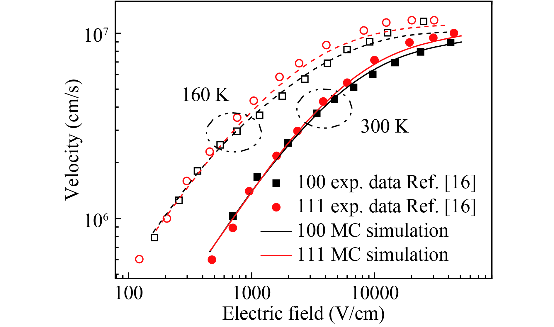
Fig. 2.  (Color online) Electron drift velocity as function of electric field at 160 and 300 K. Circles and squares refer to experimental data with the field parallel to (111) and (100) directions, respectively[16]. Solid and dashed lines indicate the calculated results using the anisotropic 3D Monte Carlo simulator.

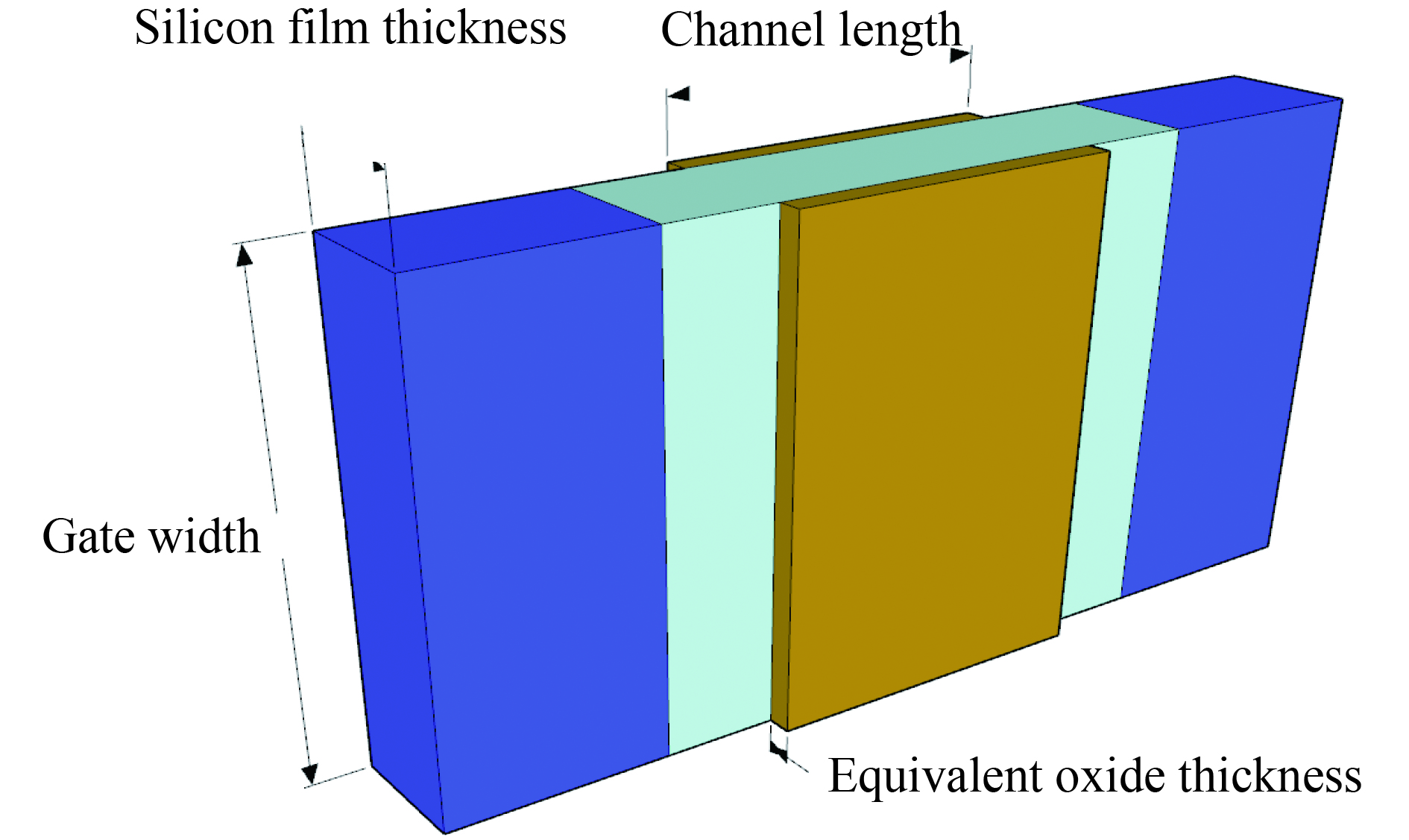
Fig. 3.  (Color online) The schematic view of DG-MOSFET structure.

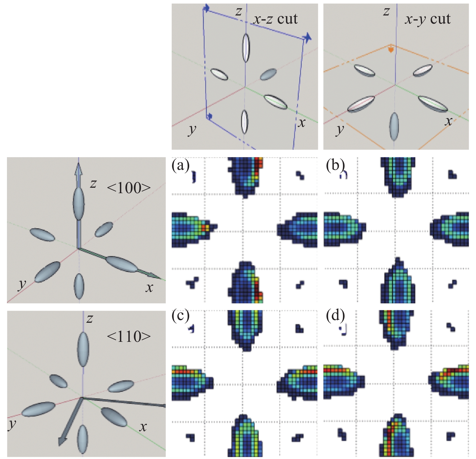
Fig. 1.  (Color online) Electron distribution in momentum space (2-D cut in x–z & x–y plane) at ~100 kV/cm electric field along the (a) & (b) <100> and (c) & (d) <110> direction at 300 K. Red is high electron density and blue is low electron density.

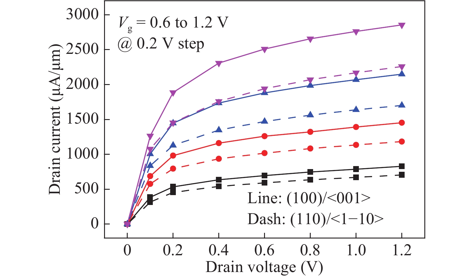
Fig. 4.  (Color online) IdVd characteristics for (100) and (110) surface devices with Vg varying from 0.6 to 1.2 V.

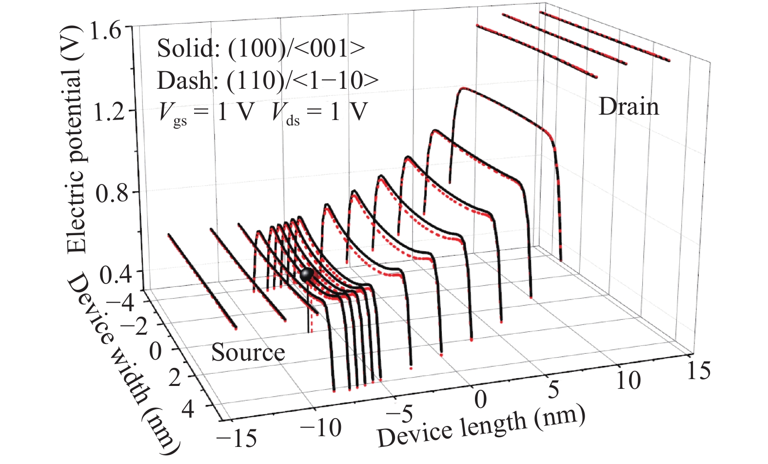
Fig. 5.  (Color online) Electrostatic potential along the channel direction for (100) and (110) surface with Vgs = 1 V and Vds = 1 V.

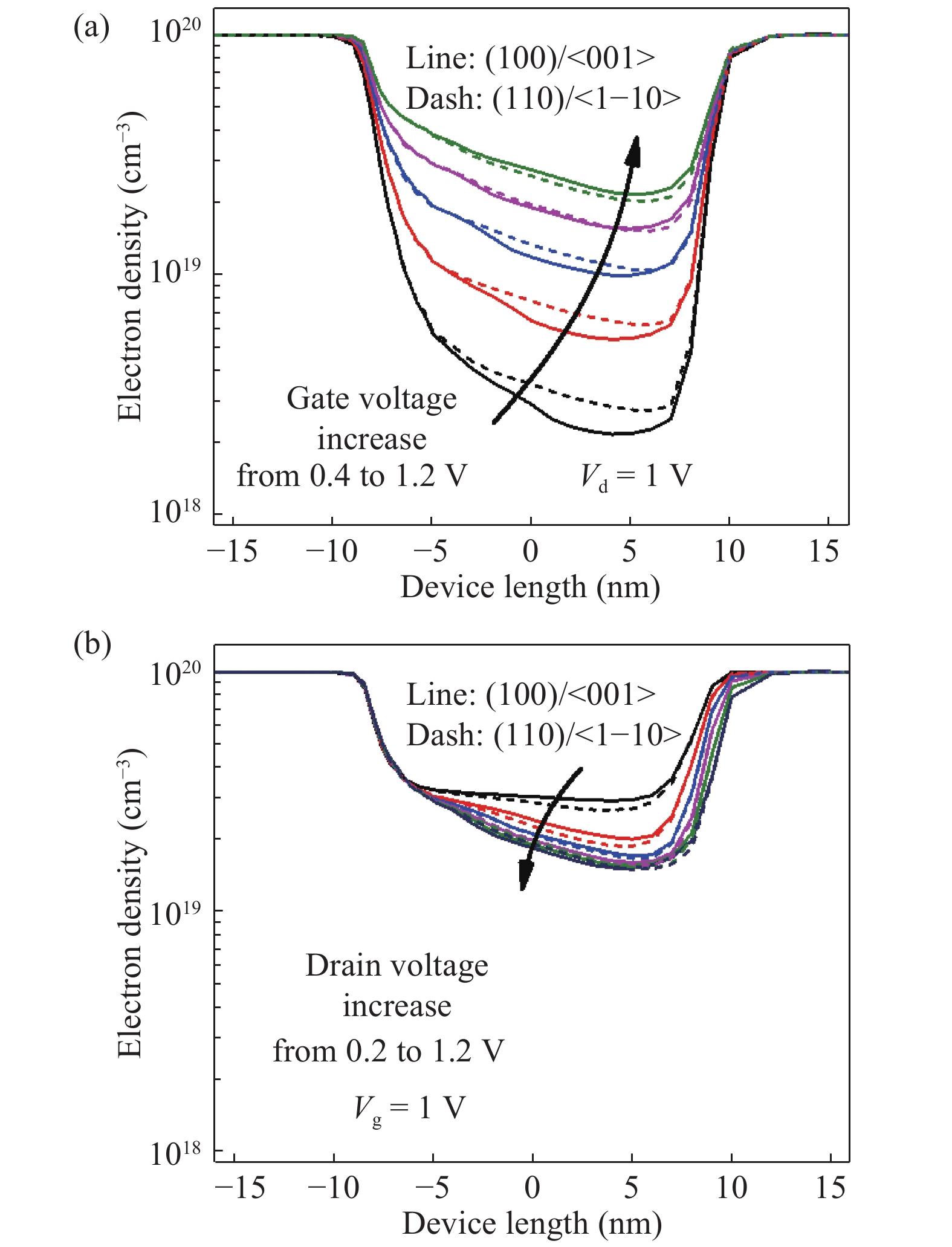
Fig. 6.  (Color online) Electron density along the channel direction for (100) and (110) surface with (a) different gate voltages and (b) different drain voltages.

Fig. 7.  (Color online) Electron velocity along the channel direction for (100) and (110) surface with (a) different gate voltages and (b) different drain voltages.

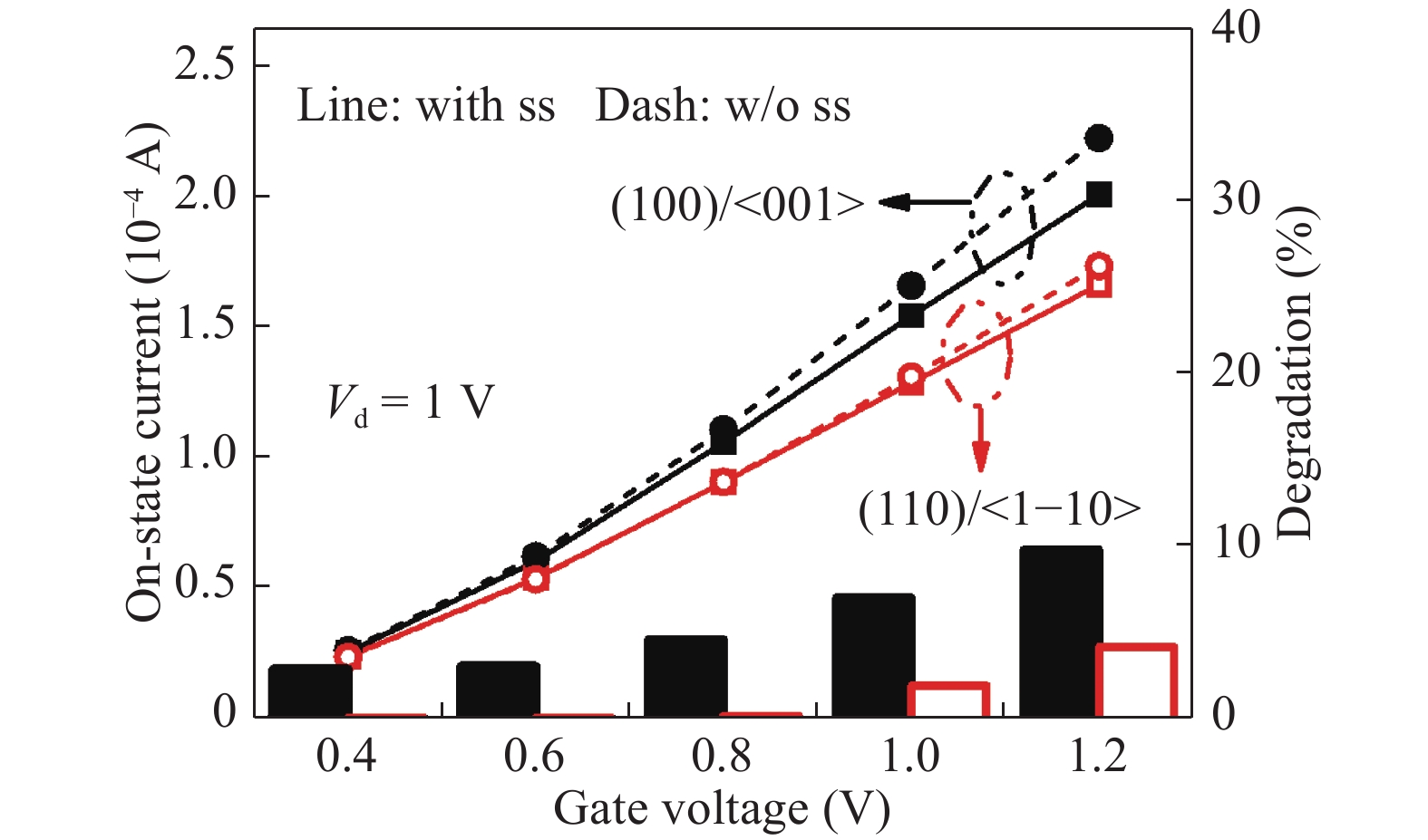
Fig. 8.  (Color online) The on-state current and degradation with Vg varies from 0.4 to 1.2 V with different surface orientation and with and without surface scattering.

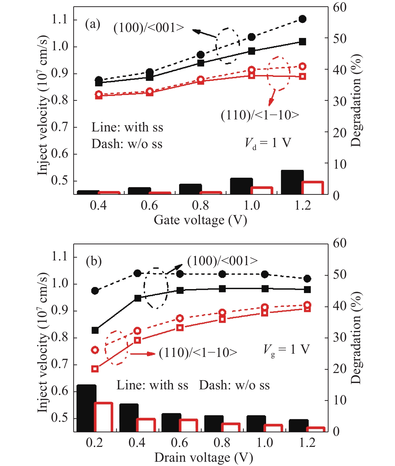
Fig. 9.  (Color online) The inject velocity and degradation with different surface orientation and with and without surface scattering.

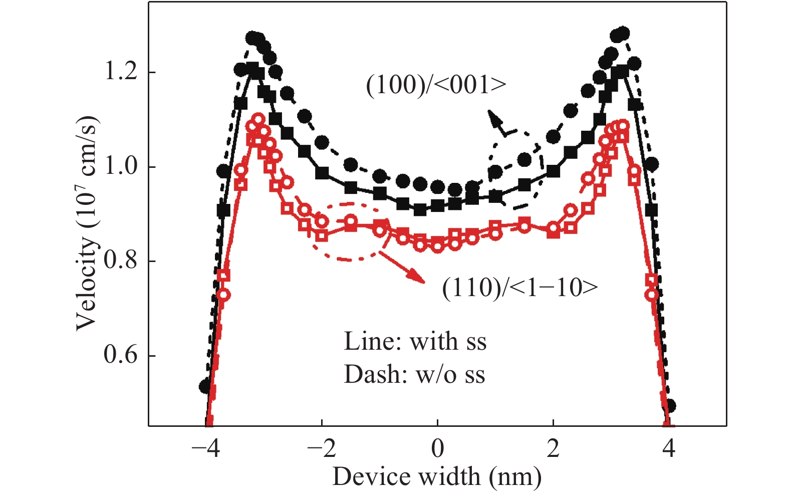
Fig. 10.  (Color online) Cross section of electron velocity at the potential barrier with different surface orientation and surface scattering.

Table 1.   Parameters in surface scattering model[17].

Parameter Value
L (nm) 2.0
Δ (nm) 0.1126755
Ξph (eV) 12.0
γ 1.5
δ 2.857703
DownLoad: CSV

Table 2.   Device parameters.

Parameter Value
Channel length (nm) 16
Silicon film thickness (nm) 8
Gate width (nm) 40
Equivalent oxide thickness (nm) 1
Channel doping (cm−3) 1016
Drain & source doping (cm −3) 1020
DownLoad: CSV
[1]
Auth C, Allen C, Blattner A, et al. A 22 nm high performance and low-power CMOS technology featuring fully-depleted tri-gate transistors, self-aligned contacts and high density MIM capacitors. Symposium on VLSI Technology, 2012: 131
[2]
Loubet N, Hook T, Montanini P, et al. Stacked nanosheet gate-all-around transistor to enable scaling beyond FinFET. Symposium on VLSI Technology, 2017: 230
[3]
Gamiz F, Donetti L, Rodriguez N. Anisotropy of electron mobility in arbitrarily oriented FinFETs. Solid State Device Research Conference, 2007: 378
[4]
Akarvardar K, Young C D, Baykan M O, et al. Impact of Fin doping and gate stack on FinFET (110) and (100) electron and hole mobilities. IEEE Electron Device Lett, 2012, 33(3): 351 doi: 10.1109/LED.2011.2182603
[5]
Young C D, Baykan M O, Agrawal A, et al. Critical discussion on (100) and (110) orientation dependent transport: nMOS planar and FinFET. Symposium on VLSI Technology, 2011, 53(2): 18
[6]
Iwai H. Future of nano CMOS technology. Solid-State Electron, 2015, 112: 56 doi: 10.1016/j.sse.2015.02.005
[7]
Lundstrom M, Ren Z. Essential physics of carrier transport in nanoscale MOSFETs. IEEE Trans Electron Devices, 2002, 49(1): 133 doi: 10.1109/16.974760
[8]
Rahman A, Guo J, Datta S, et al. Theory of ballistic nanotransistors. IEEE Trans Electron Devices, 2003, 50(9): 1853 doi: 10.1109/TED.2003.815366
[9]
Cheng R, Yu X, Chen B, et al. Investigation of self-heating effect on ballistic transport characterization for Si FinFETs featuring ultrafast pulsed IV technique. IEEE Trans Electron Devices, 2017, 64(3): 909 doi: 10.1109/TED.2016.2646907
[10]
Liu H W, Wang R S, Huang R, et al. Low-field mobility and carrier transport mechanism transition in nanoscale MOSFETs. J Semicond, 2010, 31(4): 044006 doi: 10.1088/1674-4926/31/4/044006
[11]
Chang P, Liu X, Di S, et al. Evaluation of ballistic transport in III–V-based p-channel MOSFETs. IEEE Trans Electron Devices, 2017, 64(3): 1053
[12]
Yin L, Shen L, Di S, et al. Investigation of thermal effects on FinFETs in the quasi-ballistic regime. International Conference on Solid State Devices and Materials, 2017
[13]
Shen L, Di S, Yin L, et al. Parameter calibration of drift-diffusion model in quasi-ballisitc transport region with Monte Carlo method. Silicon Nanoelectronics Workshop, 2017
[14]
Du G, Zhang W, Wang J, et al. Study of 20 nm bulk FINFET by using 3D full band Monte Carlo method with effective potential quantum correction. IEEE International Conference on Solid-State and Integrated Circuit Technology, 2010: 1952
[15]
Rahman A, Lundstrom M S, Ghosh A W. Generalized effective-mass approach for n-type metal-oxide-semiconductor field-effect transistors on arbitrarily oriented wafers. J Appl Phys, 2005, 97(5): 053702
[16]
Canali C, Jacoboni C, Nava F, et al. Electron drift velocity in silicon. Phys Rev B, 1975, 12(6): 2265 doi: 10.1103/PhysRevB.12.2265
[17]
Grgee D, Jungemann C, Nguyen C D, et al. An accurate and efficient surface scattering model for Monte Carlo device simulation. International Conference on Solid-State and Integrated Circuits Technology, 2004
  • Search

    Advanced Search >>

    GET CITATION

    shu

    Export: BibTex EndNote

    Article Metrics

    Article views: 4890 Times PDF downloads: 76 Times Cited by: 0 Times

    History

    Received: 23 October 2017 Revised: 05 January 2018 Online: Accepted Manuscript: 10 February 2018Uncorrected proof: 12 April 2018Published: 01 July 2018

    Catalog

      Email This Article

      User name:
      Email:*请输入正确邮箱
      Code:*验证码错误
      Lei Shen, Shaoyan Di, Longxiang Yin, Yun Li, Xiaoyan Liu, Gang Du. Impact of crystal orientation and surface scattering on DG-MOSFETs in quasi-ballistic region[J]. Journal of Semiconductors, 2018, 39(7): 074002. doi: 10.1088/1674-4926/39/7/074002 ****L Shen, S Y Di, L X Yin, Y Li, X Y Liu, G Du, Impact of crystal orientation and surface scattering on DG-MOSFETs in quasi-ballistic region[J]. J. Semicond., 2018, 39(7): 074002. doi: 10.1088/1674-4926/39/7/074002.
      Citation:
      Lei Shen, Shaoyan Di, Longxiang Yin, Yun Li, Xiaoyan Liu, Gang Du. Impact of crystal orientation and surface scattering on DG-MOSFETs in quasi-ballistic region[J]. Journal of Semiconductors, 2018, 39(7): 074002. doi: 10.1088/1674-4926/39/7/074002 ****
      L Shen, S Y Di, L X Yin, Y Li, X Y Liu, G Du, Impact of crystal orientation and surface scattering on DG-MOSFETs in quasi-ballistic region[J]. J. Semicond., 2018, 39(7): 074002. doi: 10.1088/1674-4926/39/7/074002.

      Impact of crystal orientation and surface scattering on DG-MOSFETs in quasi-ballistic region

      DOI: 10.1088/1674-4926/39/7/074002
      Funds:

      Project supported by the National High-Tech R&D Program (No. 2015AA016501).

      More Information
      • Corresponding author: Email: gangdu@pku.edu.cn
      • Received Date: 2017-10-23
      • Revised Date: 2018-01-05
      • Published Date: 2018-07-01

      Catalog

        /

        DownLoad:  Full-Size Img  PowerPoint
        Return
        Return