J. Semicond. > 2018, Volume 39 > Issue 7 > 074003

SEMICONDUCTOR DEVICES

Research on the hydrogen terminated single crystal diamond MOSFET with MoO3 dielectric and gold gate metal

Zeyang Ren, Jinfeng Zhang, Jincheng Zhang, Chunfu Zhang, Pengzhi Yang, Dazheng Chen, Yao Li and Yue Hao

+ Author Affiliations

 Corresponding author: Jinfeng Zhang, Email: jfzhang@xidian.edu.cn; Jincheng Zhang, jchzhang@xidian.edu.cn

DOI: 10.1088/1674-4926/39/7/074003

PDF

Turn off MathJax

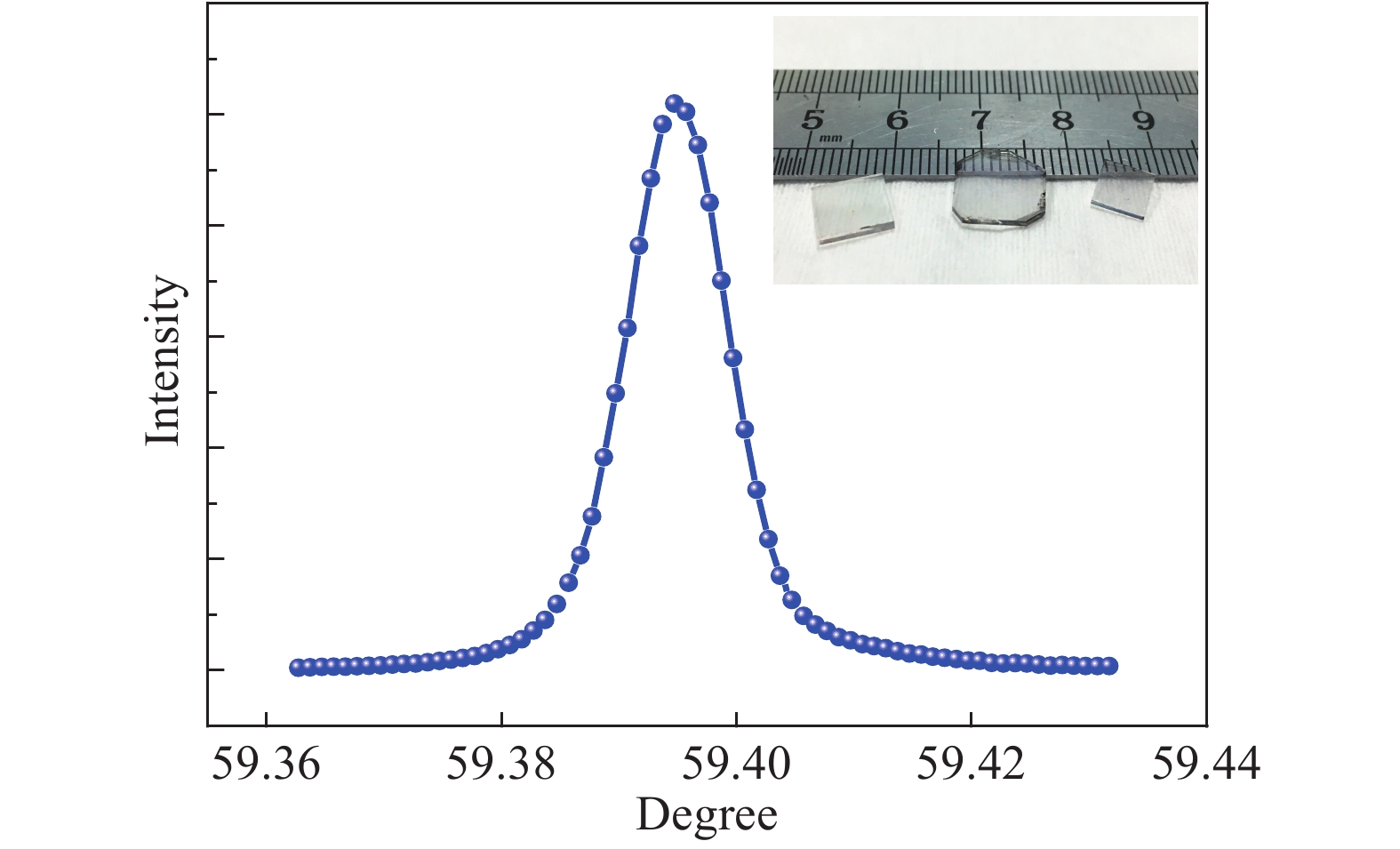
Abstract: The single crystal diamond with maximum width about 10 mm has been grown by using microwave plasma chemical vapor deposition equipment. The quality of the grown diamond was characterized using an X-ray diffractometer. The FWHM of the (004) rocking curve is 37.91 arcsec, which is comparable to the result of the electronic grade single crystal diamond commercially obtained from Element Six Ltd. The hydrogen terminated diamond field effect transistors with Au/MoO3 gates were fabricated based on our CVD diamond and the characteristics of the device were compared with the prototype Al/MoO3 gate. The device with the Au/MoO3 gate shows lower on-resistance and higher gate leakage current. The detailed analysis indicates the presence of aluminum oxide at the Al/MoO3 interface, which has been directly demonstrated by characterizing the interface between Al and MoO3 by X-ray photoelectron spectroscopy. In addition, there should be a surface transfer doping effect of the MoO3 layer on H-diamond even with the atmospheric-adsorbate induced 2DHG preserved after MoO3 deposition.

Key words: single crystal diamondMOSFETMoO3transfer doping


[1]
Liu J, Ohata H, Liao M, et al. Logic circuits with hydrogenated diamond field-effect transistors. IEEE Electron Device Lett, 2017, 38(7): 922 doi: 10.1109/LED.2017.2702744
[2]
Yamada H, Chaykhana A, Umezawa H, et al. Fabrication and fundamental characterizations of tiled clones of single-crystal diamond with 1-inch size. Diamond Relat Mater, 2012, 24: 29 doi: 10.1016/j.diamond.2011.09.007
[3]
Yamasaki S, Gheeraert E, Koide Y. Doping and interface of homoepitaxial diamond for electronic applications. Mrs Bulletin, 2014, 39(6): 499 doi: 10.1557/mrs.2014.100
[4]
Yamada H, Chayahara A, Mokuno Y, et al. A 2-in. mosaic wafer made of a single-crystal diamond. Appl Phys Lett, 2014, 104(10): 201 doi: 10.1063/1.4868720
[5]
Landstrass M I, Ravi K V. Resistivity of chemical vapor deposited diamond films. Appl Phys Lett, 1989, 55(10): 975 doi: 10.1063/1.101694
[6]
Russell S A O, Cao L, Qi D, et al. Surface transfer doping of diamond by MoO3: A combined spectroscopic and Hall measurement study. Appl Phys Lett, 2013, 103(20): 22
[7]
Crawford K G, Cao L, Qi D, et al. Enhanced surface transfer doping of diamond by V2O5 with improved thermal stability. Appl Phys Lett, 2016, 108(4): 22
[8]
He B, Ng T W, Lo M F, et al. Surface transfer doping of cubic boron nitride films by MoO3 and tetrafluoro-tetracyanoquinodimethane (F4-TCNQ). Acs Appl Mater Interfaces, 2015, 7(18): 9851 doi: 10.1021/acsami.5b01779
[9]
Russell S A O, Sharabi S, Tallaire A, et al. Hydrogen-terminated diamond field-effect transistors with cutoff frequency of 53 GHz. IEEE Electron Device Lett, 2012, 33(10): 1471 doi: 10.1109/LED.2012.2210020
[10]
Ueda K, Kasu M, Yamauchi Y, et al. Diamond FET using high-quality polycrystalline diamond with fT of 45 GHz and fmax of 120 GHz. IEEE Electron Device Lett, 2006, 27(7): 570 doi: 10.1109/LED.2006.876325
[11]
Syamsul M, Kitabayashi Y, Takuya K, et al. High voltage stress induced in transparent polycrystalline diamond field-effect transistor and enhanced endurance using thick Al2O3 passivation layer. IEEE Electron Device Lett, 2017, 38(5): 607 doi: 10.1109/LED.2017.2685081
[12]
Russell S A O, Cao L, Qi D, et al. Surface transfer doping of diamond by MoO3: A combined spectroscopic and Hall measurement study. Appl Phys Lett, 2013, 103(20): 202112 doi: 10.1063/1.4832455
[13]
Tordjman M, Saguy C, Bolker A, et al. Superior surface transfer doping of diamond with MoO3. Adv Mater Interfaces, 2014, 1(3): 1300155 doi: 10.1002/admi.201300155
[14]
Ren Z, Zhang J, Zhang J, et al. Diamond field effect transistors with MoO3 gate dielectric. IEEE Electron Device Lett, 2017, 38(6): 786 doi: 10.1109/LED.2017.2695495
[15]
Liu J W, Liao M Y, Imura M, et al. Normally-off HfO2-gated diamond field effect transistors. Appl Phys Lett, 2013, 103(9): 1899
[16]
Liu J, Liao M, Imura M, et al. Low on-resistance diamond field effect transistor with high-k ZrO2 as dielectric. Sci Rep, 2014, 4(7416): 6395
[17]
Madelung O, Rössler U, Schulz M. MoO3: optical properties, dielectric constants. Landolt-Börnstein - Group III Condensed Matter, 2000, 41d: 1
[18]
Wang J J, He Z Z, Yu C, et al. Rapid deposition of polycrystalline diamond film by DC arc plasma jet technique and its RF MESFETs. Diamond Relat Mater, 2014, 43(2): 43
[19]
Calvani P, Girolami M, Trucchi D M, et al. DC and RF performance of surface channel MESFETs on H-terminated polycrystalline diamond. Diamond Relat Mater, 2009, 18(5): 786
[20]
Kasu M, Kobayashi N. High mobility and high crystalline-quality chemical-vapor-deposition grown homoepitaxial diamond. Diamond Relat Mater, 2003, 12(3): 413
Fig. 1.  (Color online) Schematic diagram of the device fabrication processes.

Fig. 2.  (Color online) XRD result of (004) rocking curve of the CVD grown SCD.

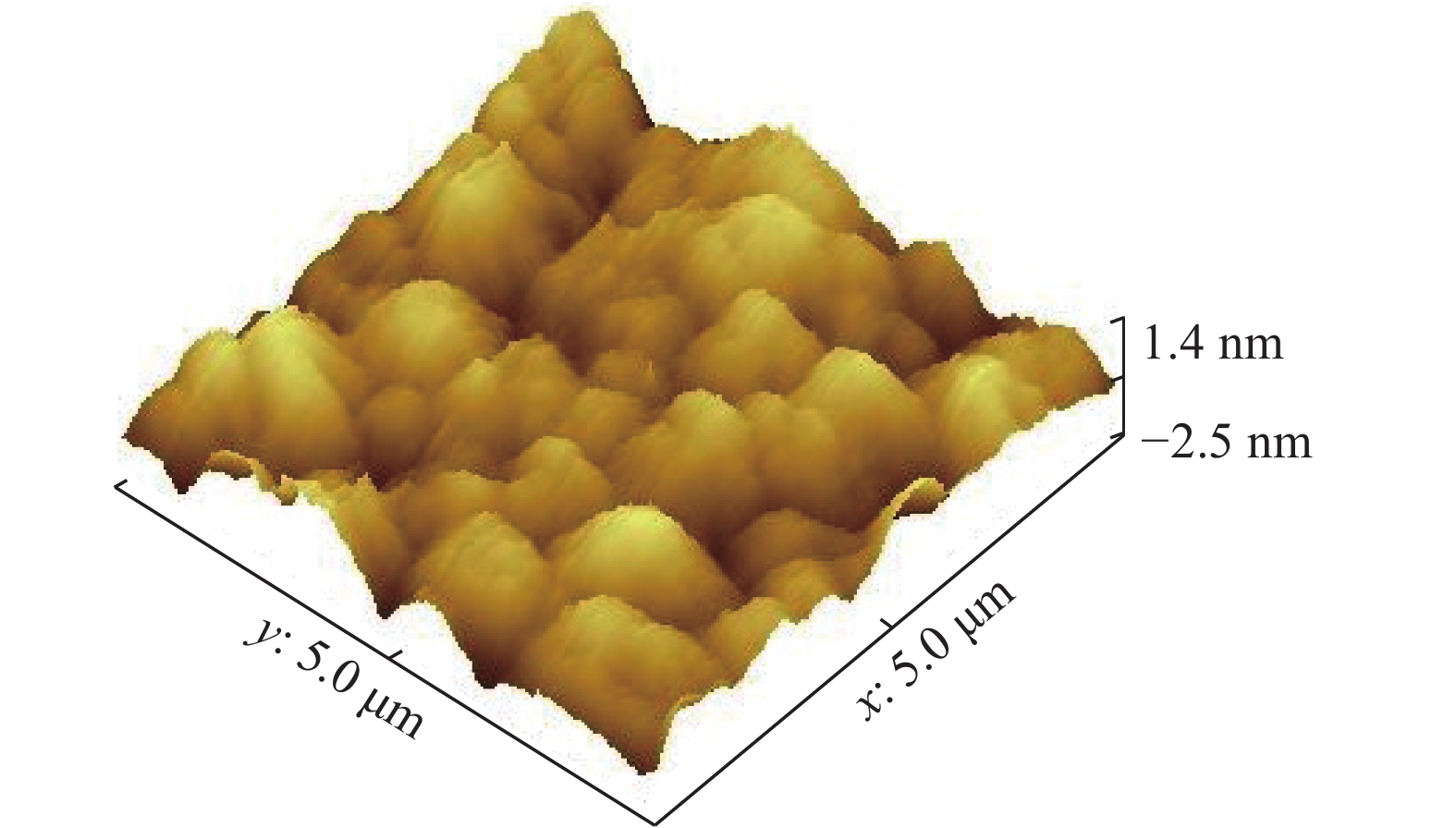
Fig. 3.  (Color online) Surface morphology of the SCD after hydrogen plasma treatment.

Fig. 4.  Surface morphology of the (a) 10 nm and (b) 40 nm MoO3 layer.

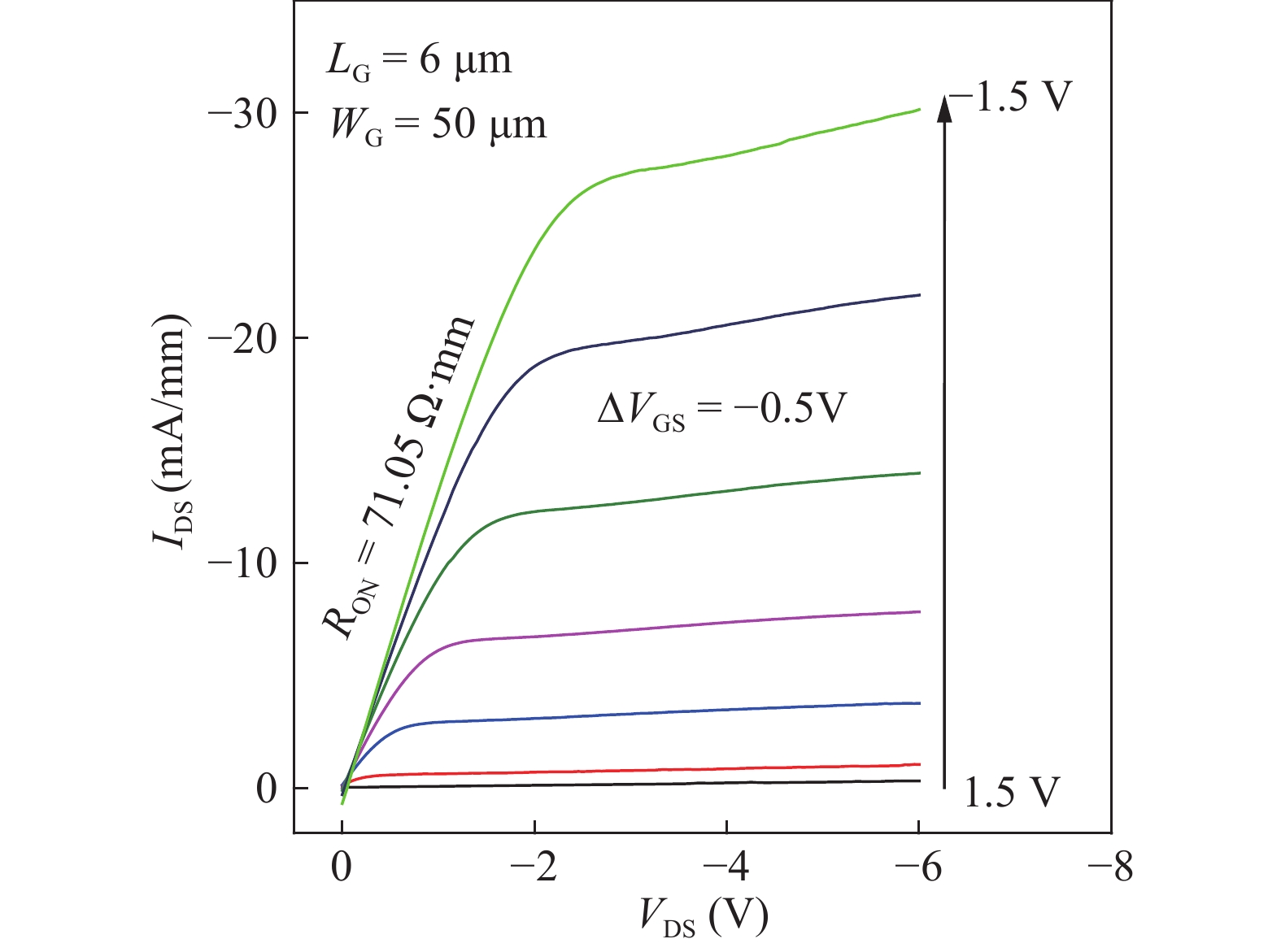
Fig. 5.  (Color online) Output characteristics of the H-diamond MOSFET.

Fig. 6.  (Color online) Gate current–voltage characteristics of the MoO3/H-diamond MOS structure.

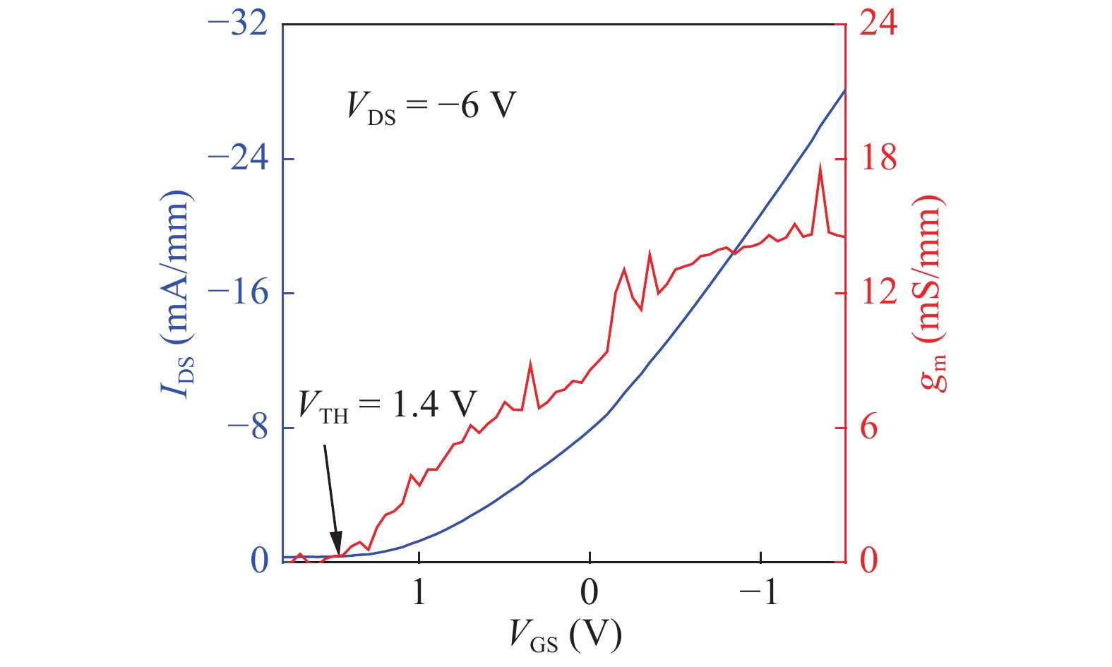
Fig. 7.  (Color online) Transfer characteristics of the H-diamond MOSFET.

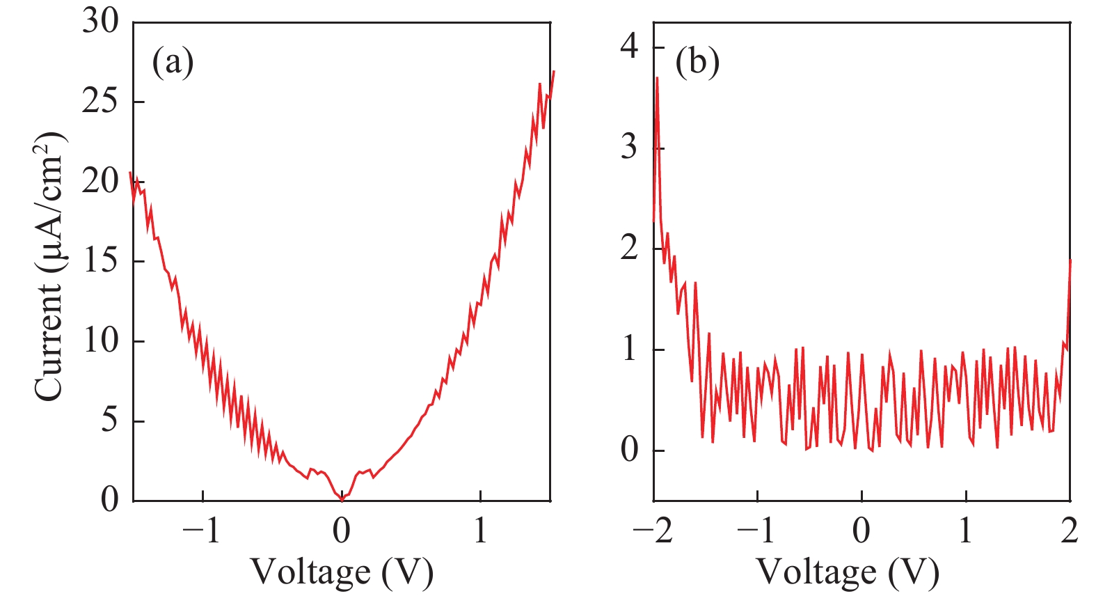
Fig. 8.  (Color online) The IV curve of (a) Au/MoO3/Au and (b) Al/MoO3/Au structure.

Fig. 9.  (Color online) XPS results of the Al metal surface, inner of the Al metal and the interface between Al and MoO3.

Fig. 10.  (Color online) Spectrum of the Al related peaks of (a) the Al metal surface, (b) the inner of the Al metal, and (c) the interface between Al and MoO3.

[1]
Liu J, Ohata H, Liao M, et al. Logic circuits with hydrogenated diamond field-effect transistors. IEEE Electron Device Lett, 2017, 38(7): 922 doi: 10.1109/LED.2017.2702744
[2]
Yamada H, Chaykhana A, Umezawa H, et al. Fabrication and fundamental characterizations of tiled clones of single-crystal diamond with 1-inch size. Diamond Relat Mater, 2012, 24: 29 doi: 10.1016/j.diamond.2011.09.007
[3]
Yamasaki S, Gheeraert E, Koide Y. Doping and interface of homoepitaxial diamond for electronic applications. Mrs Bulletin, 2014, 39(6): 499 doi: 10.1557/mrs.2014.100
[4]
Yamada H, Chayahara A, Mokuno Y, et al. A 2-in. mosaic wafer made of a single-crystal diamond. Appl Phys Lett, 2014, 104(10): 201 doi: 10.1063/1.4868720
[5]
Landstrass M I, Ravi K V. Resistivity of chemical vapor deposited diamond films. Appl Phys Lett, 1989, 55(10): 975 doi: 10.1063/1.101694
[6]
Russell S A O, Cao L, Qi D, et al. Surface transfer doping of diamond by MoO3: A combined spectroscopic and Hall measurement study. Appl Phys Lett, 2013, 103(20): 22
[7]
Crawford K G, Cao L, Qi D, et al. Enhanced surface transfer doping of diamond by V2O5 with improved thermal stability. Appl Phys Lett, 2016, 108(4): 22
[8]
He B, Ng T W, Lo M F, et al. Surface transfer doping of cubic boron nitride films by MoO3 and tetrafluoro-tetracyanoquinodimethane (F4-TCNQ). Acs Appl Mater Interfaces, 2015, 7(18): 9851 doi: 10.1021/acsami.5b01779
[9]
Russell S A O, Sharabi S, Tallaire A, et al. Hydrogen-terminated diamond field-effect transistors with cutoff frequency of 53 GHz. IEEE Electron Device Lett, 2012, 33(10): 1471 doi: 10.1109/LED.2012.2210020
[10]
Ueda K, Kasu M, Yamauchi Y, et al. Diamond FET using high-quality polycrystalline diamond with fT of 45 GHz and fmax of 120 GHz. IEEE Electron Device Lett, 2006, 27(7): 570 doi: 10.1109/LED.2006.876325
[11]
Syamsul M, Kitabayashi Y, Takuya K, et al. High voltage stress induced in transparent polycrystalline diamond field-effect transistor and enhanced endurance using thick Al2O3 passivation layer. IEEE Electron Device Lett, 2017, 38(5): 607 doi: 10.1109/LED.2017.2685081
[12]
Russell S A O, Cao L, Qi D, et al. Surface transfer doping of diamond by MoO3: A combined spectroscopic and Hall measurement study. Appl Phys Lett, 2013, 103(20): 202112 doi: 10.1063/1.4832455
[13]
Tordjman M, Saguy C, Bolker A, et al. Superior surface transfer doping of diamond with MoO3. Adv Mater Interfaces, 2014, 1(3): 1300155 doi: 10.1002/admi.201300155
[14]
Ren Z, Zhang J, Zhang J, et al. Diamond field effect transistors with MoO3 gate dielectric. IEEE Electron Device Lett, 2017, 38(6): 786 doi: 10.1109/LED.2017.2695495
[15]
Liu J W, Liao M Y, Imura M, et al. Normally-off HfO2-gated diamond field effect transistors. Appl Phys Lett, 2013, 103(9): 1899
[16]
Liu J, Liao M, Imura M, et al. Low on-resistance diamond field effect transistor with high-k ZrO2 as dielectric. Sci Rep, 2014, 4(7416): 6395
[17]
Madelung O, Rössler U, Schulz M. MoO3: optical properties, dielectric constants. Landolt-Börnstein - Group III Condensed Matter, 2000, 41d: 1
[18]
Wang J J, He Z Z, Yu C, et al. Rapid deposition of polycrystalline diamond film by DC arc plasma jet technique and its RF MESFETs. Diamond Relat Mater, 2014, 43(2): 43
[19]
Calvani P, Girolami M, Trucchi D M, et al. DC and RF performance of surface channel MESFETs on H-terminated polycrystalline diamond. Diamond Relat Mater, 2009, 18(5): 786
[20]
Kasu M, Kobayashi N. High mobility and high crystalline-quality chemical-vapor-deposition grown homoepitaxial diamond. Diamond Relat Mater, 2003, 12(3): 413
  • Search

    Advanced Search >>

    GET CITATION

    shu

    Export: BibTex EndNote

    Article Metrics

    Article views: 3900 Times PDF downloads: 50 Times Cited by: 0 Times

    History

    Received: 20 August 2017 Revised: 05 February 2018 Online: Published: 01 July 2018

    Catalog

      Email This Article

      User name:
      Email:*请输入正确邮箱
      Code:*验证码错误
      Zeyang Ren, Jinfeng Zhang, Jincheng Zhang, Chunfu Zhang, Pengzhi Yang, Dazheng Chen, Yao Li, Yue Hao. Research on the hydrogen terminated single crystal diamond MOSFET with MoO3 dielectric and gold gate metal[J]. Journal of Semiconductors, 2018, 39(7): 074003. doi: 10.1088/1674-4926/39/7/074003 ****Z Y Ren, J F Zhang, J C Zhang, C F Zhang, P Z Yang, D Z Chen, Y Li, Y Hao, Research on the hydrogen terminated single crystal diamond MOSFET with MoO3 dielectric and gold gate metal[J]. J. Semicond., 2018, 39(7): 074003. doi: 10.1088/1674-4926/39/7/074003.
      Citation:
      Zeyang Ren, Jinfeng Zhang, Jincheng Zhang, Chunfu Zhang, Pengzhi Yang, Dazheng Chen, Yao Li, Yue Hao. Research on the hydrogen terminated single crystal diamond MOSFET with MoO3 dielectric and gold gate metal[J]. Journal of Semiconductors, 2018, 39(7): 074003. doi: 10.1088/1674-4926/39/7/074003 ****
      Z Y Ren, J F Zhang, J C Zhang, C F Zhang, P Z Yang, D Z Chen, Y Li, Y Hao, Research on the hydrogen terminated single crystal diamond MOSFET with MoO3 dielectric and gold gate metal[J]. J. Semicond., 2018, 39(7): 074003. doi: 10.1088/1674-4926/39/7/074003.

      Research on the hydrogen terminated single crystal diamond MOSFET with MoO3 dielectric and gold gate metal

      DOI: 10.1088/1674-4926/39/7/074003
      More Information

      Catalog

        /

        DownLoad:  Full-Size Img  PowerPoint
        Return
        Return