| Citation: |
Tsung-Han Yang, Houqiang Fu, Hong Chen, Xuanqi Huang, Jossue Montes, Izak Baranowski, Kai Fu, Yuji Zhao. Temperature-dependent electrical properties of β-Ga2O3 Schottky barrier diodes on highly doped single-crystal substrates[J]. Journal of Semiconductors, 2019, 40(1): 012801. doi: 10.1088/1674-4926/40/1/012801
****
T Yang, H Q Fu, H Chen, X Q Huang, J Montes, I Baranowski, K Fu, Y J Zhao, Temperature-dependent electrical properties of β-Ga2O3 Schottky barrier diodes on highly doped single-crystal substrates[J]. J. Semicond., 2019, 40(1): 012801. doi: 10.1088/1674-4926/40/1/012801.
|
Temperature-dependent electrical properties of β-Ga2O3 Schottky barrier diodes on highly doped single-crystal substrates
DOI: 10.1088/1674-4926/40/1/012801
More Information
-
Abstract
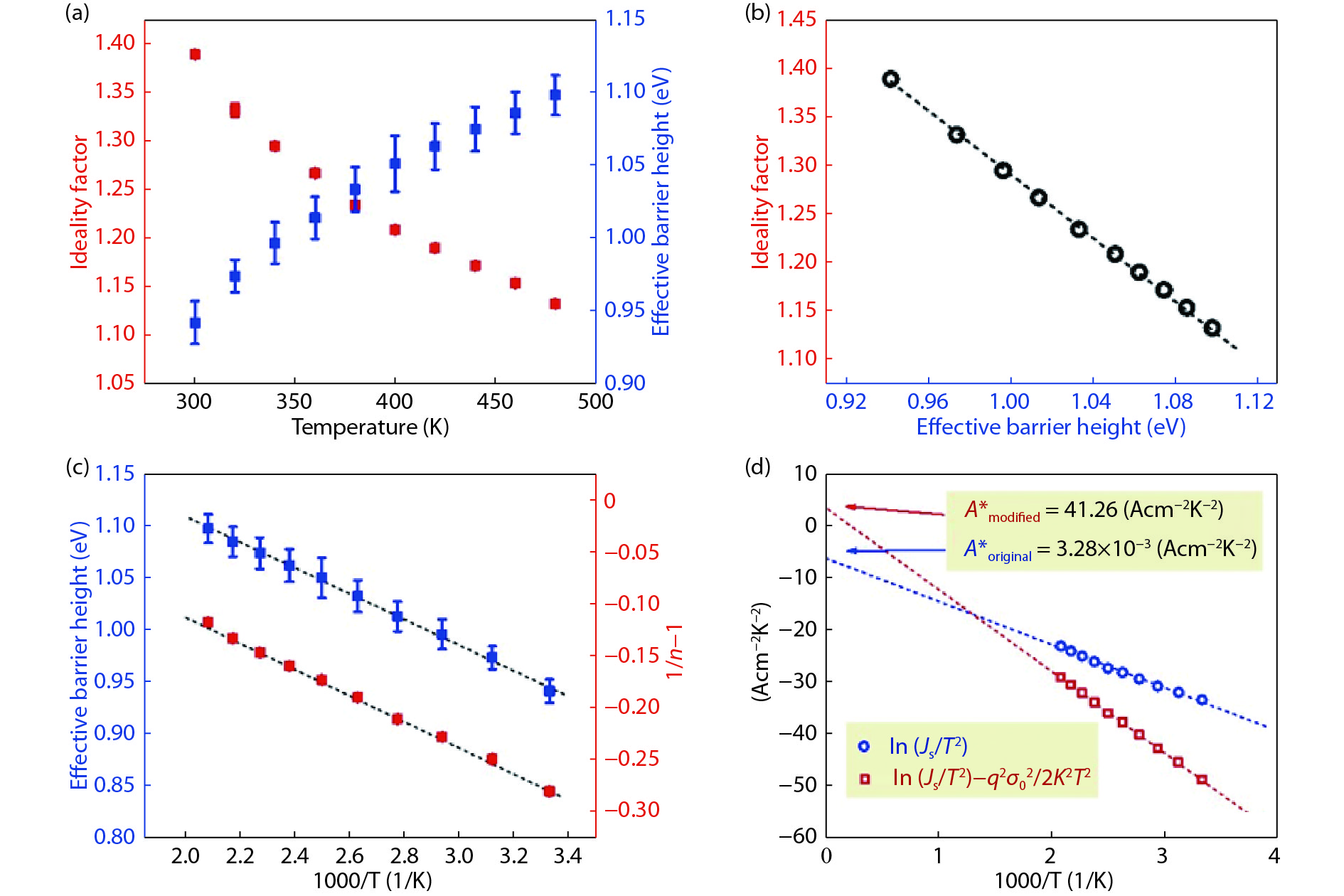
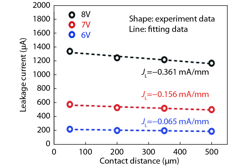
Beta-phase gallium oxide (β-Ga2O3) Schottky barrier diodes were fabricated on highly doped single-crystal substrates, where their temperature-dependent electrical properties were comprehensively investigated by forward and reverse current density – voltage and capacitance – voltage characterization. Both the Schottky barrier height and the ideality factor showed a temperature-dependence behavior, revealing the inhomogeneous nature of the Schottky barrier interface caused by the interfacial defects. With a voltage-dependent Schottky barrier incorporated into thermionic emission theory, the inhomogeneous barrier model can be further examined. Furthermore, the reverse leakage current was found to be dominated by the bulk leakage currents due to the good material and surface quality. Leakage current per distance was also obtained. These results can serve as important references for designing efficient β-Ga2O3 electronic and optoelectronic devices on highly doped substrates or epitaxial layers. -
References
[1] H Sun, K H Li, C G T Castanedo, et al. HCl flow-induced phase change of α-, β-, and ε- Ga2O3 films grown by MOCVD. Cryst Growth Design, 2018, 18: 2370 doi: 10.1021/acs.cgd.7b01791[2] H Sun, C G T Castanedo, K Liu, et al. Valence and conduction band offsets of β-Ga2O3/AlN heterojunction. Appl Phys Lett, 2017, 111: 162105, doi: 10.1063/1.5003930[3] Z Zhang, E Farzana, A Arehart, et al. Deep level defects throughout the bandgap of (010) β- Ga2O3 detected by optically and thermally stimulated defect spectroscopy. Appl Phys Lett, 2016, 108: 052105, doi: 10.1063/1.4941429[4] Q He, W Mu, H Dong, et al. Schottky barrier diode based on β-Ga2O3 (100) single crystal substrate and its temperature-dependent electrical characteristics. Appl Phys Lett, 2017, 110: 093503, doi: 10.1063/1.4977766[5] H Tippins. Optical absorption and photoconductivity in the band edge of β-Ga2O3. Phys Rev, 1965, 140: A316, doi: 10.1103/PhysRev.140.A316[6] M Higashiwaki, K Sasaki, A Kuramata, et al. Gallium oxide (Ga2O3) metal-semiconductor field-effect transistors on single-crystal β-Ga2O3 (010) substrates. Appl Phys Lett, 2012, 100: 013504, doi: 10.1063/1.3674287[7] M Higashiwaki, K Sasaki, T Kamimura, et al. Depletion-mode Ga2O3 metal–oxide–semiconductor field-effect transistors on β-Ga2O3 (010) substrates and temperature dependence of their device characteristics. Appl Phys Lett, 2013, 103: 123511, doi: 10.1063/1.4821858[8] T Oishi, Y Koga, K Harada, et al. High-mobility β-Ga2O3 ($\bar 2$ 01) single crystals grown by edge-defined film-fed growth method and their Schottky barrier diodes with Ni contact. Appl Phys Express, 2015, 8: 031101, doi: 10.7567/APEX.8.031101[9] A Kuramata, K Koshi, S Watanabe, et al. High-quality β-Ga2O3 single crystals grown by edge-defined film-fed growth. Jpn J Appl Phys, 2016, 55: 1202A2,[10] T Oishi, K Harada, Y Koga, et al. Conduction mechanism in highly doped β-Ga2O3 single crystals grown by edge-defined film-fed growth method and their Schottky barrier diodes. Jpn J Appl Phys, 2016, 55: 030305, doi: 10.7567/JJAP.55.030305[11] M Higashiwaki, K Konishi, K Sasaki, et al. Temperature-dependent capacitance–voltage and current–voltage characteristics of Pt/Ga2O3 (001) Schottky barrier diodes fabricated on n-Ga2O3 drift layers grown by halide vapor phase epitaxy. Appl Phys Lett, 2016, 108: 133503, doi: 10.1063/1.4945267[12] S Oh, M A Mastro, M J Tadjer, et al. Solar-blind metal-semiconductor-metal photodetectors based on an exfoliated β-Ga2O3 micro-flake. ECS J Solid State Sci Technol, 2017, 6: Q79 doi: 10.1149/2.0231708jss[13] M Higashiwaki, K Sasaki, A Kuramata, et al. Development of gallium oxide power devices. Phys Status Solidi A, 2014, 211: 21 doi: 10.1002/pssa.201330197[14] K Sasaki, A. Kuramata, T Masui, et al. Device-quality β-Ga2O3 epitaxial films fabricated by ozone moleular beam epitaxy. Appl Phys Express, 2012, 5: 035502, doi: 10.1143/APEX.5.035502[15] S Ahn, F Ren, L Yuan, et al. Temperature-dependent characteristics of Ni/Au and Pt/Au Schottky diodes on β-Ga2O3. ECS J Solid State Sci Technol, 2017, 6: P68 doi: 10.1149/2.0291701jss[16] K Sasaki, D Wakimoto, Q T Thieu, et al. First demonstration of Ga2O3 trench MOS-type Schottky barrier diodes. IEEE Electron Device Lett, 2017, 38: 783 doi: 10.1109/LED.2017.2696986[17] J Yang, S Ahn, F Ren, et al. High reverse breakdown voltage Schottky rectifiers without edge termination on Ga2O3. Appl Phys Lett, 2017, 110: 192101, doi: 10.1063/1.4983203[18] K Sasaki, M Higashiwaki, A Kuramata, et al. Ga2O3 Schottky barrier diodes fabricated by using single-crystal β-Ga2O3 (010) substrates. IEEE Electron Device Lett, 2013, 34: 493 doi: 10.1109/LED.2013.2244057[19] J Yang, S Ahn, F Ren, et al. High breakdown voltage (−201) β-Ga2O3 Schottky rectifiers. IEEE Electron Device Lett, 2017, 38: 906, doi: 10.1109/LED.2017.2703609[20] B Song, A K Verma, K Nomoto, et al. Vertical Ga2O3 Schottky barrier diodes on single-crystal β-Ga2O3 (−201) substrates. Device Research Conference (DRC), 2016, 2016: 1[21] H Fu, X Huang, H Chen, et al. Ultra-low turn-on voltage and on-resistance vertical GaN-on-GaN Schottky power diodes with high mobility double drift layers. Appl Phys Lett, 2017, 111: 152102, doi: 10.1063/1.4993201[22] F Iucolano, F. Roccaforte, F Giannazzo, et al. Barrier inhomogeneity and electrical properties of Pt/Ga N Shottky contacts. J Appl Phys, 2007, 102: 113701, doi: 10.1063/1.2817647[23] Y Son, R L Peterson. The effects of localized tail states on charge transport mechanisms in amorphous zinc tin oxide Schottky diodes. Semicond Sci Technol, 2017, 32: 12LT02,[24] D H Lee, K Nomura, T Kamiya, et al. Diffusion-limited a-IGZO/Pt Schottky junction fabricated at 200 °C on a flexible substrate. IEEE Electron Device Lett, 2011, 32: 1695 doi: 10.1109/LED.2011.2167123[25] J H Werner, H H Güttler. Barrier inhomogeneities at Schottky contacts. J Appl Phys, 1991, 69: 1522, doi: 10.1063/1.347243[26] H von Wenckstern, G Biehne, R A Rahman, et al. Mean barrier height of Pd Schottky contacts on ZnO thin films. Appl Phys Lett, 2006, 88: 092102, doi: 10.1063/1.2180445[27] H Fu, I Baranowski, X Huang, et al. Demonstration of AlN Schottky barrier diodes with blocking voltage over 1 kV. IEEE Electron Device Lett, 2017, 38: 1286, doi: 10.1109/LED.2017.2723603[28] E Miller, E Yu, P Waltereit, et al. Analysis of reverse-bias leakage current mechanisms in GaN grown by molecular-beam epitaxy. Appl Phys Lett, 2004, 84: 535, doi: 10.1063/1.1644029[29] F Padovani, R Stratton Field and thermionic-field emission in Schottky barriers. Solid-State Electron, 1966, 9: 695 doi: 10.1016/0038-1101(66)90097-9[30] E Miller, X Dang, E Yu Gate leakage current mechanisms in AlGaN/GaN heterostructure field-effect transistors. J Appl Phys, 2000, 88: 5951 doi: 10.1063/1.1319972[31] H Iwano, S Zaima, Y Yasuda. Hopping conduction and localized states in p-Si wires formed by focused ion beam implantations. J Vac Sci Technol B, 1998, 16: 2551 doi: 10.1116/1.590208[32] W Lu, L Wang, S Gu, et al. Analysis of reverse leakage current and breakdown voltage in GaN and InGaN/GaN Schottky barriers. IEEE Trans Electron Devices, 2011, 58: 1986 doi: 10.1109/TED.2011.2146254[33] H Fu, X Huang, H Chen, et al. Fabrication and characterization of ultra-wide bandgap AlN-based Schottky diodes on sapphire by MOCVD. IEEE J Electron Devices Soc, 2017, 5: 518 doi: 10.1109/JEDS.2017.2751554[34] T Loh, H Nguyen, R Murthy, et al. Selective epitaxial germanium on silicon-on-insulator high speed photodetectors using low-temperature ultrathin Si0.8Ge0.2 buffer. Appl Phys Lett, 2007, 91: 073503, doi: 10.1063/1.2769750[35] D Yu, C Wang, B L Wehrenberg, et al. Variable range hopping conduction in semiconductor nanocrystal solids. Phys Rev Lett, 2004, 92: 216802 doi: 10.1103/PhysRevLett.92.216802 -
Proportional views


 DownLoad:
