Processing math: 100%
J. Semicond. > 2019, Volume 40 > Issue 1 > 012802

ARTICLES

β-Ga2O3 thin film grown on sapphire substrate by plasma-assisted molecular beam epitaxy

Jiaqi Wei, Kumsong Kim, Fang Liu, Ping Wang, Xiantong Zheng, Zhaoying Chen, Ding Wang, Ali Imran, Xin Rong, Xuelin Yang, Fujun Xu, Jing Yang, Bo Shen and Xinqiang Wang

+ Author Affiliations

 Corresponding author: Xinqiang Wang, Email: wangshi@pku.edu.cn

DOI: 10.1088/1674-4926/40/1/012802

PDF

Turn off MathJax

Abstract: Monoclinic gallium oxide (Ga2O3) has been grown on (0001) sapphire (Al2O3) substrate by plasma-assisted molecular beam epitaxy (PA-MBE). The epitaxial relationship has been confirmed to be [010]( ˉ201 ) β-Ga2O3||[ 01ˉ10 ](0001)Al2O3 via in-situ reflection high energy electron diffraction (RHEED) monitoring and ex-situ X-ray diffraction (XRD) measurement. Crystalline quality is improved and surface becomes flatter with increasing growth temperature, with a best full width at half maximum (FWHM) of XRD ω-rocking curve of ( ˉ201 ) plane and root mean square (RMS) roughness of 0.68° and 2.04 nm for the sample grown at 730 °C, respectively. Room temperature cathodoluminescence measurement shows an emission at ~417 nm, which is most likely originated from recombination of donor–acceptor pair (DAP).

Key words: β-Ga2O3sapphire substratePA-MBEcrystalline qualityCL measurement

β-Ga2O3, a semiconductor with a bandgap energy of 4.6–4.9 eV at 300 K[1, 2], exhibits a great breakdown electric field of 6–8 MV/cm[3, 4] and high transparency in the deep ultraviolet (UV) and visible wavelength region. Therefore, β-Ga2O3 is attracting interest for solar-blind UV photodetectors[1, 5], gas sensors[6], transparent conducting films for electrodes on a variety of Schottky barrier diode (SBD)[4, 7, 8], metal–semiconductor field effect transistors (MESFETs)[9], metal oxide semiconductor field-effect transistors (MOSFETs)[4, 9], high dielectric oxide or active material for FET device and so on[1012]. Another important feature of Ga2O3 is that its substrate can be fabricated at low cost from bulk single crystal using the same methods such as floating zone (FZ)[13] and the edge-defined film-fed growth (EFG)[2, 14, 15] employed for manufacturing sapphire substrate, which provides a potential in mass production at low cost.

Many techniques have been employed to prepare Ga2O3 thin films, including sol-gel methods[16, 17], magnetron sputtering[18, 19], metal-organic chemical vapor deposition (MOCVD)[2022], pulsed laser deposition (PLD)[2325] and molecular beam epitaxy[2628]. Among them, MBE is an ideal technology for the growth of high quality and high purity Ga2O3 thin films due to ultrahigh vacuum growth environment and precise controllability on the growth parameters, though the growth rate is lower than some other growth methods such as MOCVD[22]. However, it is still a challenge to grow high quality β-Ga2O3 thin film on sapphire substrate, due to the large lattice mismatch between the β-Ga2O3 and sapphire.

In this paper, we report the systematical study on growth of β-Ga2O3 thin film on (0001) Al2O3 substrate by PA-MBE. It was found that crystal quality and surface flatness were improved with increasing growth temperature up to 730 °C, with a best full width at half maximum (FWHM) of XRD ω-rocking curve of ( ˉ201 ) plane and root mean square (RMS) roughness of 0.68° and 2.04 nm, respectively. Room temperature cathodoluminescence measurement shows an emission at ~417 nm, which is most likely originated from the recombination of acceptor or donor–acceptor pair (DAP).

Ga2O3 thin films are grown on (0001) plane sapphire substrate by PREVAC PA-MBE. The Ga beam is supplied by a conventional Knudsen-cell and the flux is modified by the temperature of Ga-cell. O atoms are supplied by a radio frequency plasma cell for oxygen gas, with a constant oxygen flux of 2 sccm and a forward plasma power of 280 W. The typical growth time is 200 min for all films. Reflection high-energy electron diffraction (RHEED) was used to monitor the growth process. The crystal structure and surface morphology were analyzed by X-ray diffraction (XRD), scanning electron microcopy (SEM) and atomic force microscopy (AFM). Cathodoluminescence (CL) measurement was performed at room temperature to characterize emission of the Ga2O3 thin films.

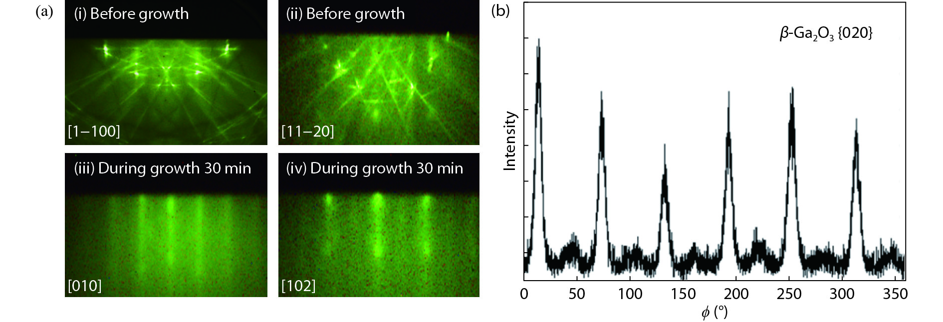
The whole growth procedure was in-situ monitored by RHEED. Fig. 1(a) shows the evolution of RHEED patterns before and after the deposition of Ga2O3 and displays that the films are single crystal. The typical RHEED patterns of sapphire (0001) plane along [ 1ˉ100 ] and [ 11ˉ20 ] azimuths were clearly observed before the growth of Ga2O3. As soon as the deposition of Ga2O3 starts, the bright fringes of sapphire were gradually transformed into faint streaky patterns. Fig. 1(a) (iii) and (iv) exhibit the RHEED patterns of Ga2O3 recorded at the same electron injection directions as those in Fig. 1(a) (i) and (ii), respectively. Compared with the patterns from sapphire substrate, not only the pattern intensity dimmed, but also the fringe spacing changed, indicating that new crystal structure is appeared. Taking into account the rectangle arranged in-plane atoms, one can easily predict that the RHEED patterns shown in Fig. 1(a) (iii) and (iv) were collected along the [010] and [102] azimuth ofβ-Ga2O3, respectively. And the epitaxial relationship between sapphire and Ga2O3 should be [010]( ˉ201 )β-Ga2O3||[ 1ˉ100 ](0001)Al2O3 and [102]( ˉ201 )β-Ga2O3||[ 11ˉ20 ](0001)Al2O3 with the lattice mismatch value of 4.2% and 10.7%, respectively[10, 22].

Figure  1.  (Color online) (a) RHEED patterns before and after the deposition of β-Ga2O3 films. (b) XRD in-plane ϕ scan for the β-Ga2O3 film grown at substrate temperature of 630 °C.

Meanwhile, the RHEED patterns were observed periodically every 60° rotation starting at the [ 1ˉ100 ] azimuth of Al2O3, which agrees well with the in-plane XRD scan result for the film grown at 630 °C shown in Fig. 1(b). The six peaks that appear every 60° indicate 6-fold in-plane rotational symmetry. Considering the fact that monoclinic β-Ga2O3 { ˉ201 } planes originally have 2-fold in-plane rotational symmetry, it can be concluded that the grown film contains in-plane rotational domains. The appearance of rotational domains is due to the 3-fold rotational symmetry of the c-sapphire surface; that is, the originally 2-fold β-Ga2O3 epitaxially grew in the three different directions at same rates, resulting in the 6-fold rotational symmetry[26, 29].

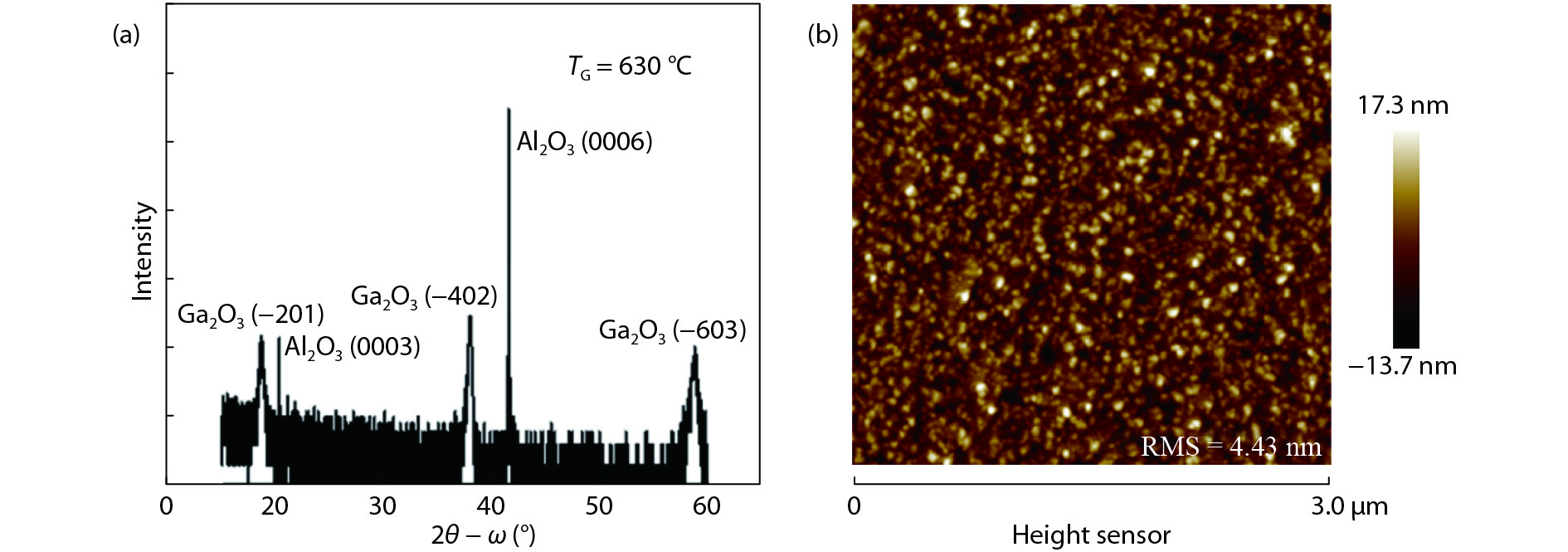
Fig. 2(a) presents the XRD 2θ–ω scan of the Ga2O3/Al2O3 sample grown at 630 °C. Comparing with the standard PDF card (No.: 43-1012)[29], the three diffraction peaks located at 18.98°, 38.48° and 59.28° can be ascribed to ( ˉ201 ), ( ˉ402 ), and ( ˉ603 ) planes of β-Ga2O3, respectively[3032]. The result indicates that the film deposited on (0001) Al2O3 substrate is pure β-Ga2O3 with single orientation along the [ ˉ201 ] direction and further confirms the predicted epitaxy relationship from the RHEED patterns.

FWHM of the XRD rocking curve obtained from the diffraction peak of ( ˉ201 ) plane was used to represent the crystal quality. The FWHM of ( ˉ201 ) of this sample is about 1.45°. According to the 3 × 3 μm2 AFM image shown in Fig. 2(b), the corresponding RMS roughness is about 4.43 nm, indicating that the crystalline quality is not satisfied. In order to improve the crystal quality and surface flatness of Ga2O3 epilayer, the growth conditions need to be optimized.

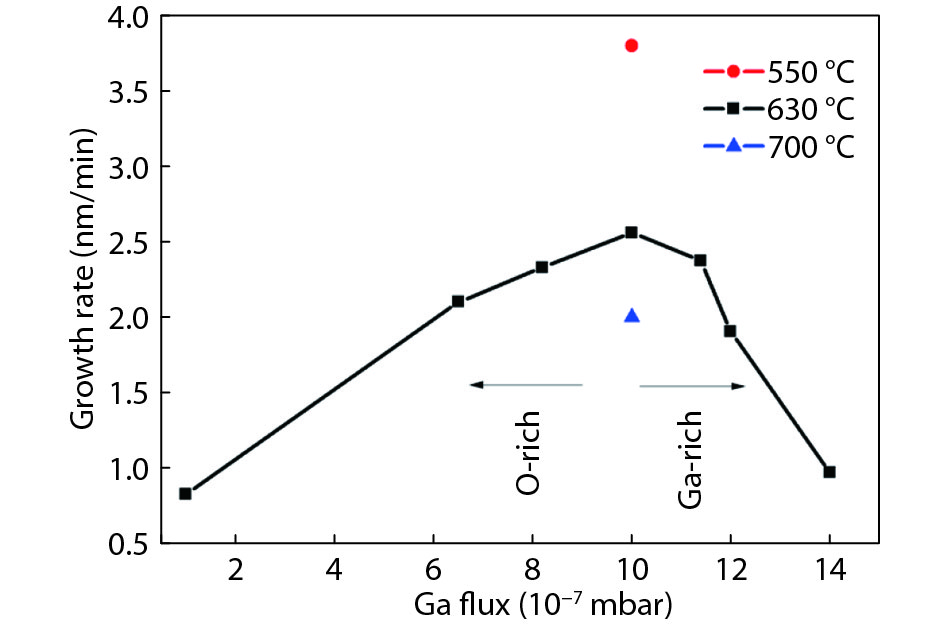
To optimize the efficient Ga to O atoms ratio, the growth temperature was maintained at 630 °C where the desorption of Ga adatoms nearly negligible, while the oxygen flux was kept constant at 2 sccm with forward plasma power of 280 W. The thickness of the β-Ga2O3 film was obtained by fitting the X-ray reflectivity (XRR) curve and further verified by scanning electron microscope (SEM) measurement. Even though the growth rate of β-Ga2O3 is low, it is clearly observed from the growth diagram shown in Fig. 3 that the growth rate increases almost linearly with increasing Ga flux up to 1.0 × 10⁻⁶ mbar at a fixed growth temperature of 630 °C and then the growth rate tends to decrease in the higher Ga flux. During the growth of Ga2O3, there is a competition between Ga2O3 (epilayer) and Ga2O (gas). The reactions for the layer growth and suboxide formations are[33]:

2Ga(g)+3O(g)Ga2O3(s),

(1)

2Ga(g)+1O(g)Ga2O1(g).

(2)

The labels g and s denote the gas and solid phase, respectively. The redundant Ga and O adatoms will form Ga2O, then desorb from the surface and does not contribute to the epitaxy of Ga2O3. This tendency has also been observed in other groups[26, 33], indicating that the growth rate is limited by the minority atom species on the growing surface and therefore the behavior in Fig. 3 can be classified into two regions of O-rich and Ga-rich. Since in Ref. [34], the growth around the stoichiometric region has resulted in the best quality, the optimum Ga flux was taken to be 1.0 × 10⁻⁶ mbar.

Figure  3.  (Color online) A growth diagram for the Ga2O3 MBE growth. The Ga flux dependent growth rate of Ga2O3 grown at different temperatures.

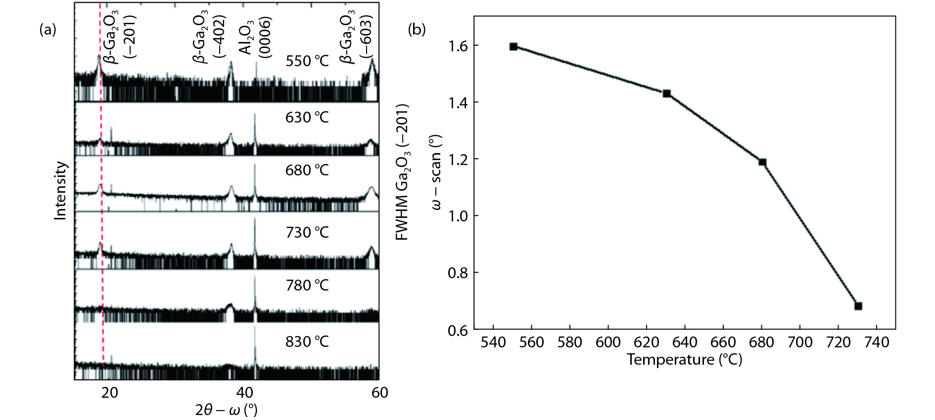
To explore the influence of growth temperature, several samples were grown at different temperatures ranging from 630 to 830 °C and the efficient Ga/O flux ratio was set at stoichiometric region. The XRD 2θ–ω scan spectra are presented in Fig. 4, Three diffraction peaks are observed in addition to the substrate’s peaks at 630 °C, 680 °C and 730 °C, which can be ascribed to the diffraction peaks from ( ˉ201 ), ( ˉ402 ) and ( ˉ603 ) planes of β-Ga2O3 with single orientation along the [ ˉ201 ] direction. Surprisingly, both of the ( ˉ201 ) and ( ˉ603 ) diffraction peaks of β-Ga2O3 disappear when the growth temperature is above 730 °C, and only the ( ˉ402 ) peak survives but tends to be annihilated. The absence of ( ˉ201 ) and ( ˉ603 ) peaks and the faint ( ˉ402 ) peak indicate the degradation of crystal structure and the reduction of growth rate due to the relatively large decomposition rate at higher growth temperature region. At higher temperature (780 °C and 830 °C), the stress caused by different coefficients of thermal expansion between film and substrate destroys the epitaxial growth, and the structure of the film changes to somehow polycrystalline[22]. The results imply that the film grown at 730 °C has optimized crystallization with an out-plane relationship of β-Ga2O3( ˉ201 )||Al2O3(0001).

Luckily, all of the diffraction peaks from β-Ga2O3 completely existed at lower growth temperature region (630–730 °C). Besides, the XRD peak intensity gradually increase and the line width gradually decrease with increasing growth temperature, indicating the improvement of crystal quality.

Fig. 4(b) shows FWHM of XRD ω-rocking curve for ( ˉ201 ) plane of β-Ga2O3 layers grown at different temperatures. Apparently, the FWHM value monotonically decreases with increasing growth temperature, and the values are 1.45°, 0.82°, and 0.68° for 630, 680, and 730 °C, respectively. The improvement of crystal quality with increasing growth temperature is a common phenomenon for materials epitaxy, but limited up to 730 °C for β-Ga2O3 in our MBE system.

Figure  4.  (Color online) (a) XRD patterns of Ga2O3 films deposited on (0001) sapphire substrates with different substrate temperatures. (b) The growth temperature dependent FWHM of XRD ω-scan for ( ˉ201 ) plane of Ga2O3 films.

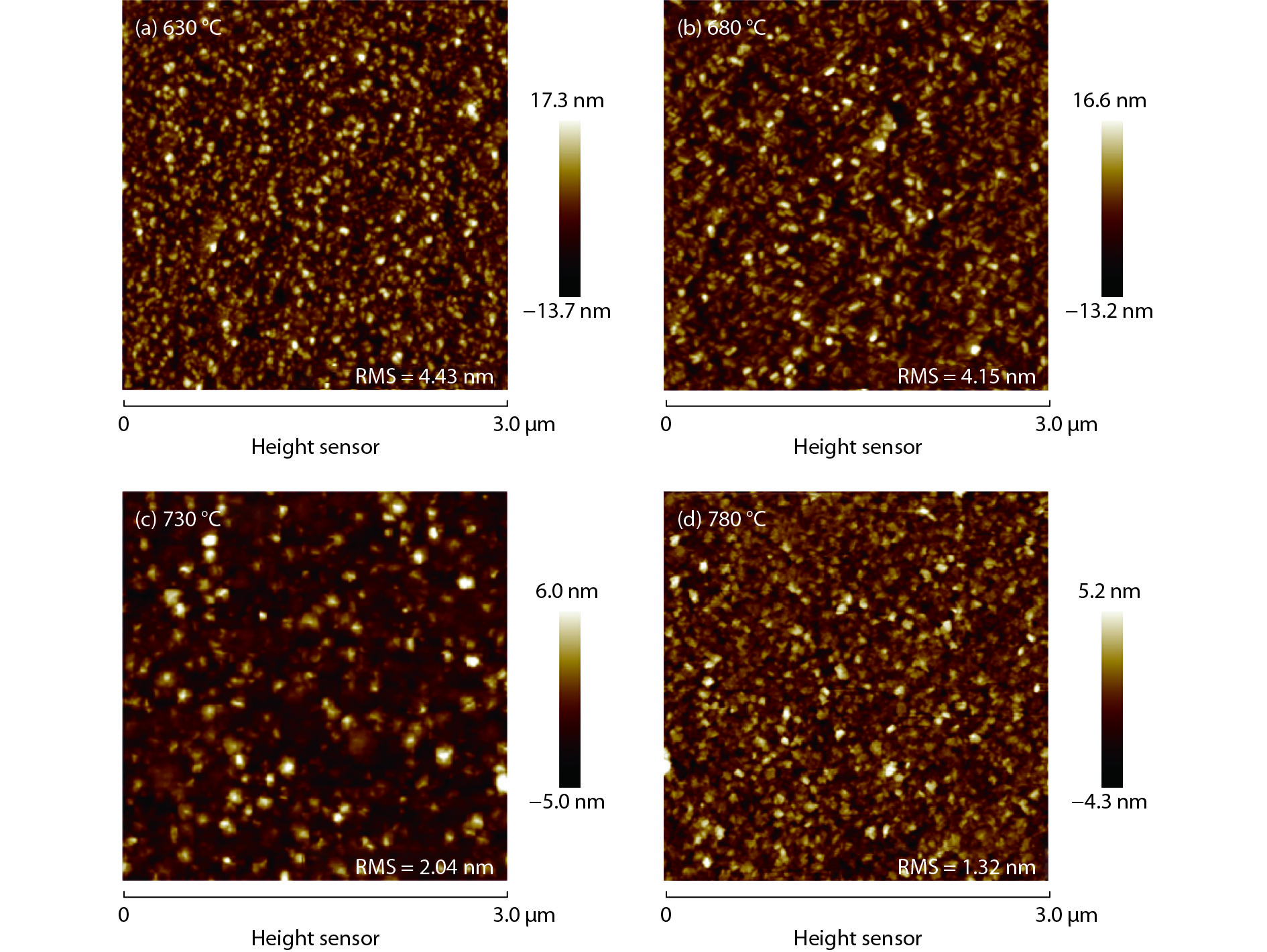
Fig. 5 shows surface morphology of Ga2O3 grown at different temperatures. Clearly, with increasing growth temperature, the RMS roughness in a scanned area of 3 × 3 μm2 gradually decreases from 4.43 nm (630 °C) to 1.32 nm (780 °C). Therefore, higher growth temperature is beneficial to improve surface flatness. Taking into account the AFM image shown in Fig. 2(b) (grown at 630 °C), all of the Ga2O3 surfaces were covered with crystal grains rather than steps. The large lattice mismatch (4.2% and 10.7%) between Ga2O3 and sapphire should be responsible for this phenomenon. Statistical analysis shows that the grain size significantly decreases with increasing growth temperature, while the grain density changes to the opposite direction. The evolution of grain size and density mainly result from the enhancement of adatoms diffusion length and the reduction of critical nucleation size with increasing growth temperature. Considering the growth rate, crystal quality, and surface flatness, the optimized growth temperature in our MBE system is 730 °C, and the corresponding Ga2O3 epilayer exhibits a FWHM of ( ˉ201 ) about 0.68° with a RMS value ~2.04 nm.

Figure  2.  (Color online) (a) XRD 2θ–ω scan of Ga2O3/ Al2O3 grown at 630 °C. (b) Surface morphology investigated by AFM in a scanned area of 3 × 3 μm2.
Figure  5.  (Color online) AFM surface morphology of β-Ga2O3 deposited at different substrate temperatures. (a) 630 °C. (b) 680 °C. (c) 730 °C. (d) 780 °C.

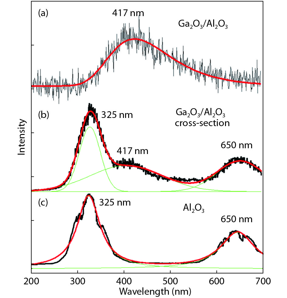
Room temperature cathodeluminescence (RT-CL) have been performed on the surface and cross section of Ga2O3/Al2O3 and Al2O3 substrate. The spectra in Fig. 6 shows a strong broad UV-blue and a weak red emission band centered at 325, 417 and 650 nm. Unfortunately, we did not find any band edge emission (240–270 nm) from these samples. Comparing with the emission behavior of sapphire substrate shown in Fig. 6(c), the emission peak in Fig. 6(b) around 325 and 650 nm mainly results from the defects in sapphire while the emission with peak at 417 nm comes from β-Ga2O3 film. This blue emission is due to recombination of electron on donor and hole at acceptor or donor–acceptor pair (DAP). These donors might be dominated by oxygen vacancies (VO) and acceptors might be created by gallium vacancies (VGa) or gallium–oxygen vacancies pair (VGa–VO)[3537]. It is clear that the quality of β-Ga2O3 film is not good enough and further study should be done to improve it.

Figure  6.  (Color online) RT-CL spectra of (a) 400-nm-thick β-Ga2O3 film, (b) cross sectional β-Ga2O3 thin film, (c) Al2O3 substrate.

In conclusion, β-Ga2O3 thin film has been grown on (0001) sapphire substrate by PA-MBE, and the epitaxial relationship is confirmed as [010]( ˉ201 )β-Ga2O3||[ 01ˉ10 ](0001)Al2O3. Crystalline quality and surface flatness have been improved with increasing growth temperature with the best FWHM of XRD ω-scans of ( ˉ201 ) plane and RMS roughness of 0.68° and 2.04 nm, respectively. RT-CL spectra suggests that the β-Ga2O3 thin film exhibits a strong defects-related emission at around 417 nm and further improvement of crystalline quality is needed.

Acknowledgements

This work was supported by the National Key R&D Program of China (No. 2018YFB0406502) and the National Natural Science Foundation of China (Nos. 61734001, 61521004).


[1]
Guo D, Wu Z, Li P, et al. Fabrication of β-Ga2O3 thin films and solar-blind photodetectors by laser MBE technology. Opt Mater Express, 2014, 4(5): 1067 doi: 10.1364/OME.4.001067
[2]
Mu W, Jia Z, Yin Y, et al. High quality crystal growth and anisotropic physical characterization of β-Ga2O3 single crystals grown by EFG method. J Alloys Compd, 2017, 714: 453 doi: 10.1016/j.jallcom.2017.04.185
[3]
Pearton S J, Yang J, Patrick C, et al. A review of Ga2O3 materials, processing, and devices. Appl Phys Rev, 2018, 5(1): 011301 doi: 10.1063/1.5006941
[4]
Xue H, He Q, Jian G, et al. An overview of the ultrawide bandgap Ga2O3 semiconductor-based schottky barrier diode for power electronics application. Nanoscale Res Lett, 2018 13: 290 doi: 10.1186/s11671-018-2712-1
[5]
Zhao X, Cui W, Wu Z, et al. Growth and characterization of Sn doped β-Ga2O3 thin films and enhanced performance in a solar-blind photodetector. J Electron Mater, 2017, 46(4): 2366 doi: 10.1007/s11664-017-5291-5
[6]
Kumar S S, Rubio E J, Noor-A-Alam M, et al. Structure, morphology, and optical properties of amorphous and nanocrystalline gallium oxide thin films. J Phys Chem C, 2013, 117(8): 4194 doi: 10.1021/jp311300e
[7]
Farzana E, Ahmadi E, Speck J S, et al. Deep level defects in Ge-doped (010) β-Ga2O3 layers grown by plasma-assisted molecular beam epitaxy. J Appl Phys, 2018, 123(16): 1
[8]
Hu Z, Zhou H, Feng Q, et al. Field-plated lateral β-Ga2O3 schottky barrier diode with high reverse blocking voltage of more than 3 kV and high DC power figure-of-merit of 500 MW/cm2. IEEE Electron Device Lett, 2018, 39(10): 1564
[9]
Higashiwaki M, Sasaki K, Kuramata A, et al. Development of gallium oxide power devices. Phys Status Solidi, 2014, 211(1): 21 doi: 10.1002/pssa.201330197
[10]
Galazka Z. β-Ga2O3 for wide-bandgap electronics and optoelectronics. Semicond Sci Technol, 2018, 33, 113001 doi: 10.1088/1361-6641/aadf78
[11]
Kumar S, Tessarek C, Christiansen S, et al. A comparative study of β-Ga2O3 nanowires grown on different substrates using CVD technique. J Alloys Compd, 2014, 587: 812 doi: 10.1016/j.jallcom.2013.10.165
[12]
Rafique S, Han L, Neal A T, et al. Towards high mobility heteroepitaxial β-Ga2O3 on sapphire-dependence on the substrate off-axis angle. Phys Status Solidi, 2018, 215(2): 1700467 doi: 10.1002/pssa.v215.2
[13]
E G Víllora, Shimamura K, Yoshikawa Y, et al. Large-size β-Ga2O3 single crystals and wafers. J Cryst Growth, 2004, 270(3/4): 420
[14]
Aida H, Nishiguchi K, Takeda H, et al. Growth of β-Ga2O3 single crystals by the edge-defined, film fed growth method. Jpn J Appl Phys, 2008, 47(11R): 8506
[15]
Higashiwaki M, Konishi K, Sasaki K, et al. Temperature-dependent capacitance-voltage and current-voltage characteristics of Pt/Ga2O3 (001) Schottky barrier diodes fabricated on n-Ga2O3 drift layers grown by halide vapor phase epitaxy. Appl Phys Lett, 2016, 108(13): 133503 doi: 10.1063/1.4945267
[16]
Sinha G, Adhikar K, Chaudhuri S, et al. Sol-gel derived phase pure α-Ga2O3 nanocrystalline thin film and its optical properties. J Cryst Growth, 2005, 276(1): 204
[17]
Kokubun Y, Miura K, Endo F, et al. Sol-gel prepared β-Ga2O3 thin films for ultraviolet photodetectors. Appl Phys Lett, 2007, 90(3): A316
[18]
Fleischer M, Hanrieder W, Meixner H. Stability of semiconducting gallium oxide thin films. Thin Solid Films, 1990, 190: 93 doi: 10.1016/0040-6090(90)90132-W
[19]
Liu J J, Yan J L, Shi L, et al. Electrical and optical properties of deep ultraviolet transparent conductive Ga2O3/ITO films by magnetron sputtering. J Semicond, 2010. 31: 103001. doi: 10.1088/1674-4926/31/10/103001
[20]
Ji Z, Du J, Fan J, et al. Gallium oxide films for filter and solar-blind UV detector. Opt Mater, 2006, 28(4): 415 doi: 10.1016/j.optmat.2005.03.006
[21]
Fleischer M, Hanrieder W, Meixner H. Stability of semiconducting gallium oxide thin films. Thin Solid Films, 2015, 190(1): 93
[22]
Lv Y, Ma J, Mi W, et al. Characterization of β-Ga2O3 thin films on sapphire (0001) using metal-organic chemical vapor deposition technique. Vacuum, 2012, 86(12): 1850 doi: 10.1016/j.vacuum.2012.04.019
[23]
Hayashi H, Huang R, Oba F, et al. Epitaxial growth of Mn-doped γ-Ga2O3 on spinel substrate. J Mater Res, 2011, 26(4): 578 doi: 10.1557/jmr.2010.32
[24]
Matsuzaki K, Hiramatsu H, Nomura K, et al. Growth, structure and carrier transport properties of Ga2O3 epitaxial film examined for transparent field-effect transistor. Thin Solid Films, 2006, 496(1): 37 doi: 10.1016/j.tsf.2005.08.187
[25]
Zhang F, Saito K, Tanaka T, et al. Electrical properties of Si doped Ga2O3 films grown by pulsed laser deposition. J Mater Sci: Mater Electron, 2015, 26(12): 9624 doi: 10.1007/s10854-015-3627-6
[26]
Oshima T, Okuno T, Fujita S. Ga2O3 thin film growth on c-plane sapphire substrates by molecular beam epitaxy for deep-ultraviolet photodetectors. Jpn J Appl Phys, 2007, 46(11): 7217 doi: 10.1143/JJAP.46.7217
[27]
Nakagomi S, Kokubun Y. Crystal orientation of β-Ga2O3 thin films formed on c-plane and a-plane sapphire substrate. J Cryst Growth, 2012, 349(1): 12 doi: 10.1016/j.jcrysgro.2012.04.006
[28]
Zhang Y, Joishi C, Xia Z, et al. Demonstration of β-(AlxGa1−x)2O3/Ga2O3 double heterostructure field effect transistors. Appl Phys Lett, 2018, 112(23): 233503 doi: 10.1063/1.5037095
[29]
Zhang F B, Saito K, Tanaka T, et al. Structural and optical properties of Ga2O3, films on sapphire substrates by pulsed laser deposition. J Cryst Growth, 2014, 387(2): 96
[30]
Huang L, Feng Q, Han G, et al. Comparison study of β-Ga2O3 photodetectors grown on sapphire at different oxygen pressures. IEEE Photonics J, 2017, 9(4): 1
[31]
Cheng Z, Hanke M, Vogt P, et al. Phase formation and strain relaxation of Ga2O3 on c-plane and a-plane sapphire substrates as studied by synchrotron-based x-ray diffraction. Appl Phys Lett, 2017, 111(16): 162104 doi: 10.1063/1.4998804
[32]
Villora E G, Shimamura K, Kitamura K, et al. Rf-plasma-assisted molecular-beam epitaxy of β-Ga2O3. Appl Phys Lett, 2006, 88(3): 841
[33]
Vogt P, Bierwagen O. Reaction kinetics and growth window for plasma-assisted molecular beam epitaxy of Ga2O3: Incorporation of Ga vs. Ga2O desorption. Appl Phys Lett, 2016, 108(7): 024001
[34]
Ravadgar P, Horng R H, Yao S D, et al. Effects of crystallinity and point defects on optoelectronic applications of β-Ga2O3 epilayers. Opt Express, 2013, 21(21): 24599 doi: 10.1364/OE.21.024599
[35]
Guzmán-Navarro G, Herrera-Zaldívar M, Valenzuela-Benavides J, et al. CL study of blue and UV emissions in β-Ga2O3 nanowires grown by thermal evaporation of GaN. J Appl Phys, 2011, 110(3): 033517 doi: 10.1063/1.3610386
[36]
Yu D P, Bubendorff J L, Zhou J F, et al. Localized cathodoluminescence investigation on single Ga2O3 nanoribbon/nanowire. Solid State Commun, 2002, 124(10/11): 417
[37]
Hao J, Cocivera M. Optical and luminescent properties of undoped and rare-earth-doped Ga2O3 thin films deposited by spray pyrolysis. J Phys D Appl Phys, 2002, 35(5): 433 doi: 10.1088/0022-3727/35/5/304
Fig. 1.  (Color online) (a) RHEED patterns before and after the deposition of β-Ga2O3 films. (b) XRD in-plane ϕ scan for the β-Ga2O3 film grown at substrate temperature of 630 °C.

Fig. 3.  (Color online) A growth diagram for the Ga2O3 MBE growth. The Ga flux dependent growth rate of Ga2O3 grown at different temperatures.

Fig. 4.  (Color online) (a) XRD patterns of Ga2O3 films deposited on (0001) sapphire substrates with different substrate temperatures. (b) The growth temperature dependent FWHM of XRD ω-scan for ( ˉ201 ) plane of Ga2O3 films.

Fig. 2.  (Color online) (a) XRD 2θ–ω scan of Ga2O3/ Al2O3 grown at 630 °C. (b) Surface morphology investigated by AFM in a scanned area of 3 × 3 μm2.

Fig. 5.  (Color online) AFM surface morphology of β-Ga2O3 deposited at different substrate temperatures. (a) 630 °C. (b) 680 °C. (c) 730 °C. (d) 780 °C.

Fig. 6.  (Color online) RT-CL spectra of (a) 400-nm-thick β-Ga2O3 film, (b) cross sectional β-Ga2O3 thin film, (c) Al2O3 substrate.

[1]
Guo D, Wu Z, Li P, et al. Fabrication of β-Ga2O3 thin films and solar-blind photodetectors by laser MBE technology. Opt Mater Express, 2014, 4(5): 1067 doi: 10.1364/OME.4.001067
[2]
Mu W, Jia Z, Yin Y, et al. High quality crystal growth and anisotropic physical characterization of β-Ga2O3 single crystals grown by EFG method. J Alloys Compd, 2017, 714: 453 doi: 10.1016/j.jallcom.2017.04.185
[3]
Pearton S J, Yang J, Patrick C, et al. A review of Ga2O3 materials, processing, and devices. Appl Phys Rev, 2018, 5(1): 011301 doi: 10.1063/1.5006941
[4]
Xue H, He Q, Jian G, et al. An overview of the ultrawide bandgap Ga2O3 semiconductor-based schottky barrier diode for power electronics application. Nanoscale Res Lett, 2018 13: 290 doi: 10.1186/s11671-018-2712-1
[5]
Zhao X, Cui W, Wu Z, et al. Growth and characterization of Sn doped β-Ga2O3 thin films and enhanced performance in a solar-blind photodetector. J Electron Mater, 2017, 46(4): 2366 doi: 10.1007/s11664-017-5291-5
[6]
Kumar S S, Rubio E J, Noor-A-Alam M, et al. Structure, morphology, and optical properties of amorphous and nanocrystalline gallium oxide thin films. J Phys Chem C, 2013, 117(8): 4194 doi: 10.1021/jp311300e
[7]
Farzana E, Ahmadi E, Speck J S, et al. Deep level defects in Ge-doped (010) β-Ga2O3 layers grown by plasma-assisted molecular beam epitaxy. J Appl Phys, 2018, 123(16): 1
[8]
Hu Z, Zhou H, Feng Q, et al. Field-plated lateral β-Ga2O3 schottky barrier diode with high reverse blocking voltage of more than 3 kV and high DC power figure-of-merit of 500 MW/cm2. IEEE Electron Device Lett, 2018, 39(10): 1564
[9]
Higashiwaki M, Sasaki K, Kuramata A, et al. Development of gallium oxide power devices. Phys Status Solidi, 2014, 211(1): 21 doi: 10.1002/pssa.201330197
[10]
Galazka Z. β-Ga2O3 for wide-bandgap electronics and optoelectronics. Semicond Sci Technol, 2018, 33, 113001 doi: 10.1088/1361-6641/aadf78
[11]
Kumar S, Tessarek C, Christiansen S, et al. A comparative study of β-Ga2O3 nanowires grown on different substrates using CVD technique. J Alloys Compd, 2014, 587: 812 doi: 10.1016/j.jallcom.2013.10.165
[12]
Rafique S, Han L, Neal A T, et al. Towards high mobility heteroepitaxial β-Ga2O3 on sapphire-dependence on the substrate off-axis angle. Phys Status Solidi, 2018, 215(2): 1700467 doi: 10.1002/pssa.v215.2
[13]
E G Víllora, Shimamura K, Yoshikawa Y, et al. Large-size β-Ga2O3 single crystals and wafers. J Cryst Growth, 2004, 270(3/4): 420
[14]
Aida H, Nishiguchi K, Takeda H, et al. Growth of β-Ga2O3 single crystals by the edge-defined, film fed growth method. Jpn J Appl Phys, 2008, 47(11R): 8506
[15]
Higashiwaki M, Konishi K, Sasaki K, et al. Temperature-dependent capacitance-voltage and current-voltage characteristics of Pt/Ga2O3 (001) Schottky barrier diodes fabricated on n-Ga2O3 drift layers grown by halide vapor phase epitaxy. Appl Phys Lett, 2016, 108(13): 133503 doi: 10.1063/1.4945267
[16]
Sinha G, Adhikar K, Chaudhuri S, et al. Sol-gel derived phase pure α-Ga2O3 nanocrystalline thin film and its optical properties. J Cryst Growth, 2005, 276(1): 204
[17]
Kokubun Y, Miura K, Endo F, et al. Sol-gel prepared β-Ga2O3 thin films for ultraviolet photodetectors. Appl Phys Lett, 2007, 90(3): A316
[18]
Fleischer M, Hanrieder W, Meixner H. Stability of semiconducting gallium oxide thin films. Thin Solid Films, 1990, 190: 93 doi: 10.1016/0040-6090(90)90132-W
[19]
Liu J J, Yan J L, Shi L, et al. Electrical and optical properties of deep ultraviolet transparent conductive Ga2O3/ITO films by magnetron sputtering. J Semicond, 2010. 31: 103001. doi: 10.1088/1674-4926/31/10/103001
[20]
Ji Z, Du J, Fan J, et al. Gallium oxide films for filter and solar-blind UV detector. Opt Mater, 2006, 28(4): 415 doi: 10.1016/j.optmat.2005.03.006
[21]
Fleischer M, Hanrieder W, Meixner H. Stability of semiconducting gallium oxide thin films. Thin Solid Films, 2015, 190(1): 93
[22]
Lv Y, Ma J, Mi W, et al. Characterization of β-Ga2O3 thin films on sapphire (0001) using metal-organic chemical vapor deposition technique. Vacuum, 2012, 86(12): 1850 doi: 10.1016/j.vacuum.2012.04.019
[23]
Hayashi H, Huang R, Oba F, et al. Epitaxial growth of Mn-doped γ-Ga2O3 on spinel substrate. J Mater Res, 2011, 26(4): 578 doi: 10.1557/jmr.2010.32
[24]
Matsuzaki K, Hiramatsu H, Nomura K, et al. Growth, structure and carrier transport properties of Ga2O3 epitaxial film examined for transparent field-effect transistor. Thin Solid Films, 2006, 496(1): 37 doi: 10.1016/j.tsf.2005.08.187
[25]
Zhang F, Saito K, Tanaka T, et al. Electrical properties of Si doped Ga2O3 films grown by pulsed laser deposition. J Mater Sci: Mater Electron, 2015, 26(12): 9624 doi: 10.1007/s10854-015-3627-6
[26]
Oshima T, Okuno T, Fujita S. Ga2O3 thin film growth on c-plane sapphire substrates by molecular beam epitaxy for deep-ultraviolet photodetectors. Jpn J Appl Phys, 2007, 46(11): 7217 doi: 10.1143/JJAP.46.7217
[27]
Nakagomi S, Kokubun Y. Crystal orientation of β-Ga2O3 thin films formed on c-plane and a-plane sapphire substrate. J Cryst Growth, 2012, 349(1): 12 doi: 10.1016/j.jcrysgro.2012.04.006
[28]
Zhang Y, Joishi C, Xia Z, et al. Demonstration of β-(AlxGa1−x)2O3/Ga2O3 double heterostructure field effect transistors. Appl Phys Lett, 2018, 112(23): 233503 doi: 10.1063/1.5037095
[29]
Zhang F B, Saito K, Tanaka T, et al. Structural and optical properties of Ga2O3, films on sapphire substrates by pulsed laser deposition. J Cryst Growth, 2014, 387(2): 96
[30]
Huang L, Feng Q, Han G, et al. Comparison study of β-Ga2O3 photodetectors grown on sapphire at different oxygen pressures. IEEE Photonics J, 2017, 9(4): 1
[31]
Cheng Z, Hanke M, Vogt P, et al. Phase formation and strain relaxation of Ga2O3 on c-plane and a-plane sapphire substrates as studied by synchrotron-based x-ray diffraction. Appl Phys Lett, 2017, 111(16): 162104 doi: 10.1063/1.4998804
[32]
Villora E G, Shimamura K, Kitamura K, et al. Rf-plasma-assisted molecular-beam epitaxy of β-Ga2O3. Appl Phys Lett, 2006, 88(3): 841
[33]
Vogt P, Bierwagen O. Reaction kinetics and growth window for plasma-assisted molecular beam epitaxy of Ga2O3: Incorporation of Ga vs. Ga2O desorption. Appl Phys Lett, 2016, 108(7): 024001
[34]
Ravadgar P, Horng R H, Yao S D, et al. Effects of crystallinity and point defects on optoelectronic applications of β-Ga2O3 epilayers. Opt Express, 2013, 21(21): 24599 doi: 10.1364/OE.21.024599
[35]
Guzmán-Navarro G, Herrera-Zaldívar M, Valenzuela-Benavides J, et al. CL study of blue and UV emissions in β-Ga2O3 nanowires grown by thermal evaporation of GaN. J Appl Phys, 2011, 110(3): 033517 doi: 10.1063/1.3610386
[36]
Yu D P, Bubendorff J L, Zhou J F, et al. Localized cathodoluminescence investigation on single Ga2O3 nanoribbon/nanowire. Solid State Commun, 2002, 124(10/11): 417
[37]
Hao J, Cocivera M. Optical and luminescent properties of undoped and rare-earth-doped Ga2O3 thin films deposited by spray pyrolysis. J Phys D Appl Phys, 2002, 35(5): 433 doi: 10.1088/0022-3727/35/5/304
1

2-inch diameter (010) principal-face β-Ga2O3 single crystals grown by EFG method

Xuyang Dong, Wenxiang Mu, Pei Wang, Yue Dong, Hao Zhao, et al.

Journal of Semiconductors, 2025, 46(6): 062501. doi: 10.1088/1674-4926/24110029

2

Two-step growth of β-Ga2O3 on c-plane sapphire using MOCVD for solar-blind photodetector

Peipei Ma, Jun Zheng, Xiangquan Liu, Zhi Liu, Yuhua Zuo, et al.

Journal of Semiconductors, 2024, 45(2): 022502. doi: 10.1088/1674-4926/45/2/022502

3

2.83-kV double-layered NiO/β-Ga2O3 vertical p-n heterojunction diode with a power figure-of-merit of 5.98 GW/cm2

Tingting Han, Yuangang Wang, Yuanjie Lv, Shaobo Dun, Hongyu Liu, et al.

Journal of Semiconductors, 2023, 44(7): 072802. doi: 10.1088/1674-4926/44/7/072802

4

Preparation and photodetection performance of high crystalline quality and large size β-Ga2O3 microwires

Yuefei Wang, Yurui Han, Chong Gao, Bingsheng Li, Jiangang Ma, et al.

Journal of Semiconductors, 2023, 44(6): 062806. doi: 10.1088/1674-4926/44/6/062806

5

Growth and characterization of β-Ga2O3 thin films grown on off-angled Al2O3 substrates by metal-organic chemical vapor deposition

Yabao Zhang, Jun Zheng, Peipei Ma, Xueyi Zheng, Zhi Liu, et al.

Journal of Semiconductors, 2022, 43(9): 092801. doi: 10.1088/1674-4926/43/9/092801

6

Morphology and crystalline property of an AlN single crystal grown on AlN seed

Li Zhang, Haitao Qi, Hongjuan Cheng, Yuezeng Shi, Zhanpin Lai, et al.

Journal of Semiconductors, 2021, 42(5): 052101. doi: 10.1088/1674-4926/42/5/052101

7

A review of β-Ga2O3 single crystal defects, their effects on device performance and their formation mechanism

Bo Fu, Zhitai Jia, Wenxiang Mu, Yanru Yin, Jian Zhang, et al.

Journal of Semiconductors, 2019, 40(1): 011804. doi: 10.1088/1674-4926/40/1/011804

8

Growth and fundamentals of bulk β-Ga2O3 single crystals

H. F. Mohamed, Changtai Xia, Qinglin Sai, Huiyuan Cui, Mingyan Pan, et al.

Journal of Semiconductors, 2019, 40(1): 011801. doi: 10.1088/1674-4926/40/1/011801

9

Catalyst-free growth of ZnO nanowires on various-oriented sapphire substrates by pulsed-laser deposition

Tetsuya Shimogaki, Masahiro Takahashi, Masaaki Yamasaki, Taichi Fukuda, Mitsuhiro Higashihata, et al.

Journal of Semiconductors, 2016, 37(2): 023001. doi: 10.1088/1674-4926/37/2/023001

10

High quality metal-quantum dot-metal structure fabricated with a highly compatible self-aligned process

Yingchun Fu, Xiaofeng Wang, Liuhong Ma, Yaling Zhou, Xiang Yang, et al.

Journal of Semiconductors, 2015, 36(12): 123004. doi: 10.1088/1674-4926/36/12/123004

11

Unstrained InAlN/GaN heterostructures grown on sapphire substrates by MOCVD

Bo Liu, Jiayun Yin, Yuanjie Lü, Shaobo Dun, Xiongwen Zhang, et al.

Journal of Semiconductors, 2014, 35(11): 113005. doi: 10.1088/1674-4926/35/11/113005

12

Effects of growth temperature on high-quality In0.2Ga0.8N layers by plasma-assisted molecular beam epitaxy

Zhang Dongyan, Zheng Xinhe, Li Xuefei, Wu Yuanyuan, Wang Jianfeng, et al.

Journal of Semiconductors, 2012, 33(10): 103001. doi: 10.1088/1674-4926/33/10/103001

13

Effect of substrate temperature on the properties of deep ultraviolet transparent conductive ITO/Ga2

Li Ting, Yan Jinliang, Ding Xingwei, Zhang Liying

Journal of Semiconductors, 2012, 33(1): 013002. doi: 10.1088/1674-4926/33/1/013002

14

Structural and optical properties of Zn-doped β-Ga2O3 films

Yue Wei, Yan Jinliang, Wu Jiangyan, Zhang Liying

Journal of Semiconductors, 2012, 33(7): 073003. doi: 10.1088/1674-4926/33/7/073003

15

Optimization of Al2O3/SiNx stacked antireflection structures for N-type surface-passivated crystalline silicon solar cells

Wu Dawei, Jia Rui, Ding Wuchang, Chen Chen, Wu Deqi, et al.

Journal of Semiconductors, 2011, 32(9): 094008. doi: 10.1088/1674-4926/32/9/094008

16

Electrical and optical properties of deep ultraviolet transparent conductive Ga2O3/ITO films by magnetron sputtering

Liu Jianjun, Yan Jinliang, Shi Liang, Li Ting

Journal of Semiconductors, 2010, 31(10): 103001. doi: 10.1088/1674-4926/31/10/103001

17

Effect of Annealing Temperature on ZnO Thin Film Grown on a TiO2 Buffer Layer

Xu Linhua, Li Xiangyin, Shi Linxing, Shen Hua

Journal of Semiconductors, 2008, 29(10): 1992-1997.

18

Synthesis and Characterization of GaN Nanorods by Ammoniating Ga2O3/Co Films Deposited on Si(111) Substrates

Qin Lixia, Xue Chengshan, Zhuang Huizhao, Yang Zhaozhu, Chen Jinhua, et al.

Journal of Semiconductors, 2008, 29(2): 210-213.

19

Dislocation Reduction in GaN on Sapphire by Epitaxial Lateral Overgrowth

Chen Jun, Wang Jianfeng, Wang Hui, Zhao Degang, Zhu Jianjun, et al.

Chinese Journal of Semiconductors , 2006, 27(3): 419-424.

20

0.25μm Gate-Length AlGaN/GaN Power HEMTs on Sapphire with fT of 77GHz

Zheng Yingkui, Liu Guoguo, He Zhijing, Liu Xinyu, Wu Dexin, et al.

Chinese Journal of Semiconductors , 2006, 27(6): 963-965.

1. Waseem, A., Latham, G.M., McAleese, C. et al. Comprehensive study of β-Ga2O3 epitaxial growth using a variable closed-coupled showerhead MOCVD reactor. Applied Physics Reviews, 2025, 12(2): 021412. doi:10.1063/5.0239454
2. Wang, L., Zhang, Y., Dong, J. et al. High-temporal dynamic self-powered β-Ga2O3/GaN heterojunction ultraviolet photodetector. Journal of Physics D: Applied Physics, 2025, 58(13): 135121. doi:10.1088/1361-6463/ada993
3. Zhang, S., Zhang, G., Wu, H. et al. Localized surface plasmon enhanced the photoresponse performance of Ga2O3 ultraviolet photodetectors. Micro and Nanostructures, 2025. doi:10.1016/j.micrna.2024.208063
4. Taboada Vasquez, J.M., Li, X. A Review of Vertical Ga2O3 Diodes: From Fabrication to Performance Optimization and Future Outlooks. Physica Status Solidi (B): Basic Research, 2025. doi:10.1002/pssb.202400635
5. Ganguly, S., Nama Manjunatha, K., Paul, S. Advances in Gallium Oxide: Properties, Applications, and Future Prospects. Advanced Electronic Materials, 2025. doi:10.1002/aelm.202400690
6. Serquen, E., Bravo, F., Chi, Z. et al. Impact of c- and m- sapphire plane orientations on the structural and electrical properties of β-Ga2O3 thin films grown by metal-organic chemical vapor deposition. Journal of Physics D: Applied Physics, 2024, 57(49): 495106. doi:10.1088/1361-6463/ad76bb
7. Aggarwal, V., Kumar, M., Kumar, R. et al. Unveiling the synergic potential of dual junction MoSe2/n-Ga2O3/p-GaN heterojunctions for ultra-broadband photodetection. Materials Advances, 2024, 5(24): 9744-9755. doi:10.1039/d4ma00934g
8. Mock, A., Richter, S., Papamichail, A. et al. Effective uniaxial dielectric function tensor and optical phonons in (2 ¯ 01)-oriented β - Ga2 O3 films with equally distributed sixfold-rotation domains. Physical Review Applied, 2024, 22(4): 044003. doi:10.1103/PhysRevApplied.22.044003
9. Yang, T., Shou, C., Almujtabi, A. et al. Beta to Spinel Phase Transition of Magnesium Gallium Oxide Thin Films and Their Photoluminescence Properties. ACS Applied Electronic Materials, 2024, 6(9): 6640-6647. doi:10.1021/acsaelm.4c01079
10. Vogt, P., Hensling, F.V.E., Azizie, K. et al. Adsorption-controlled growth of Ga2O3 by Suboxide Molecular-Beam Epitaxy. Zentropy: Tools, Modelling, and Applications, 2024.
11. Zhang, Z., Wang, T., Jiang, H. et al. Probing Hyperbolic Shear Polaritons in β-Ga2O3 Nanostructures Using STEM-EELS. Advanced Materials, 2024, 36(19): 2204884. doi:10.1002/adma.202204884
12. Li, J., Wang, Y., Li, W. et al. Effect of tin source temperature on the β-Ga2O3 film deposited by MOCVD. Materials Science and Engineering: B, 2024. doi:10.1016/j.mseb.2024.117221
13. Yadav, M.K., Mondal, A., Sharma, S.K. et al. Unveiling Thermal Effects on Sn-Doped β-Ga2O3Schottky Barrier Diodes on Sapphire for High-Temperature Power Electronics. IEEE Transactions on Electron Devices, 2024, 71(3): 1529-1534. doi:10.1109/TED.2023.3333818
14. Ganguly, S., Nama Manjunatha, K., Paul, S. Investigation on the Mist Intensity to Deposit Gallium Oxide Thin Films by Mist Chemical Vapor Deposition. Physica Status Solidi - Rapid Research Letters, 2024, 18(2): 2300296. doi:10.1002/pssr.202300296
15. Yang, T., Shou, C., Almujtabi, A. et al. Investigation of Phase Transition and Ultrawide Band Gap Engineering in MgGaO Semiconductor Thin Films. ACS Applied Optical Materials, 2023, 1(10): 1670-1678. doi:10.1021/acsaom.3c00237
16. Wang, J., Luo, T.-C., He, Y.-C. et al. Chemical reaction-mass transport model of Ga2O3 grown by TEGa in MOCVD and an intelligent system. Journal of Crystal Growth, 2023. doi:10.1016/j.jcrysgro.2023.127311
17. Wang, Z., Zhang, C., Sun, X. et al. MOCVD Epitaxy of β-Ga2O3 Films on Off-Cut Angled Sapphire Substrates and Fabrication of Solar-Blind Ultraviolet Photodetector | [切割角蓝宝石基氧化镓薄膜 MOCVD 外延及日盲紫外光电探测器制备]. Rengong Jingti Xuebao/Journal of Synthetic Crystals, 2023, 52(6): 1007-1015.
18. Yang, T., Shou, C., Xu, L. et al. Metal-Semiconductor-Metal Photodetectors Based on β-MgGaO Thin Films. ACS Applied Electronic Materials, 2023, 5(4): 2122-2130. doi:10.1021/acsaelm.3c00035
19. Fan, T., Tang, N., Wei, J. et al. Reduction of vacancy defects induced by thermal annealing in β-Ga2O3 epilayer. Micro and Nanostructures, 2023. doi:10.1016/j.micrna.2023.207525
20. Zuo, Y., Feng, Q., Zhang, T. et al. A Novel Method for Growing α-Ga2O3 Films Using Mist-CVD Face-to-face Heating Plates. Nanomaterials, 2023, 13(1): 72. doi:10.3390/nano13010072
21. Liu, Y., Wei, S., Shan, C. et al. Compositions and properties of high-conductivity nitrogen-doped p-type β-Ga2O3films prepared by the thermal oxidation of GaN in N2O ambient. Journal of Materials Research and Technology, 2022. doi:10.1016/j.jmrt.2022.10.110
22. Zhang, S., Wei, S., Liu, Z. et al. The rise of AI optoelectronic sensors: From nanomaterial synthesis, device design to practical application. Materials Today Physics, 2022. doi:10.1016/j.mtphys.2022.100812
23. Zhang, Y., Zheng, J., Ma, P. et al. Growth and characterization of β-Ga2O3 thin films grown on off-angled Al2O3 substrates by metal-organic chemical vapor deposition. Journal of Semiconductors, 2022, 43(9): 092801. doi:10.1088/1674-4926/43/9/092801
24. Chou, T.-S., Bin Anooz, S., Grüneberg, R. et al. Machine learning supported analysis of MOVPE grown β-Ga2O3 thin films on sapphire. Journal of Crystal Growth, 2022. doi:10.1016/j.jcrysgro.2022.126737
25. Schmidt, C., Zahn, D.R.T. Effect of impurities on the Raman spectra of spray-coated β-Ga2O3thin films. Journal of Vacuum Science and Technology A: Vacuum, Surfaces and Films, 2022, 40(4): 043404. doi:10.1116/6.0001822
26. Vogt, P., Hensling, F.V.E., Azizie, K. et al. Extending the Kinetic and Thermodynamic Limits of Molecular-Beam Epitaxy Utilizing Suboxide Sources or Metal-Oxide-Catalyzed Epitaxy. Physical Review Applied, 2022, 17(3): 034021. doi:10.1103/PhysRevApplied.17.034021
27. Wei, J., Liu, F., Rong, X. et al. Effect of unintentional nitrogen incorporation on n-type doping of β-Ga2O3grown by molecular beam epitaxy. CrystEngComm, 2022, 24(2): 269-274. doi:10.1039/d1ce01207j
28. Chen, X., Huet, B., Choudhury, T.H. et al. Orientation domain dispersions in wafer scale epitaxial monolayer WSe2 on sapphire. Applied Surface Science, 2021. doi:10.1016/j.apsusc.2021.150798
29. Zhang, T., Li, Y., Zhang, Y. et al. Investigation of β-Ga2O3 thin films grown on epi-GaN/sapphire(0001) substrates by low pressure MOCVD. Journal of Alloys and Compounds, 2021. doi:10.1016/j.jallcom.2020.157810
30. Hadamek, T., Posadas, A.B., Al-Quaiti, F. et al. β-Ga2O3on Si (001) grown by plasma-assisted MBE with γ-Al2O3(111) buffer layer: Structural characterization. AIP Advances, 2021, 11(4): 045209. doi:10.1063/5.0044923
31. Vogt, P., Hensling, F.V.E., Azizie, K. et al. Adsorption-controlled growth of Ga2O3by suboxide molecular-beam epitaxy. APL Materials, 2021, 9(3): 031101. doi:10.1063/5.0035469
32. Akyol, F.. Investigating the effect of self-trapped holes in the current gain mechanism of β−Ga2O3 Schottky diode photodetectors. Turkish Journal of Physics, 2021, 45(3): 169-177. doi:10.3906/fiz-2102-12
33. Zhang, T., Hu, Z., Li, Y. et al. Comparison of Ga2O3films grown on m- And r-plane sapphire substrates by MOCVD. ECS Journal of Solid State Science and Technology, 2020, 9(12): 125008. doi:10.1149/2162-8777/abd48d
34. Li, K., Yang, X., Tian, Y. et al. Ga2O3 solar-blind position-sensitive detectors. Science China: Physics, Mechanics and Astronomy, 2020, 63(11): 117312. doi:10.1007/s11433-020-1581-4
35. Wang, D., He, L., Ma, X. et al. Preparation and properties of heteroepitaxial β-Ga2O3 films on KTaO3 (100) substrates by MOCVD. Materials Characterization, 2020. doi:10.1016/j.matchar.2020.110391
36. Zhang, H., Yuan, L., Tang, X. et al. Progress of Ultra-Wide Bandgap Ga2O3 Semiconductor Materials in Power MOSFETs. IEEE Transactions on Power Electronics, 2020, 35(5): 5157-5179. doi:10.1109/TPEL.2019.2946367
37. Hao, S., Hetzl, M., Kunzelmann, V.F. et al. Sub-bandgap optical spectroscopy of epitaxial β -Ga2O3 thin films. Applied Physics Letters, 2020, 116(9): 092102. doi:10.1063/1.5143393
38. Jiao, T., Li, Z.-M., Wang, Q. et al. Growth of β-Ga2O3 Thin Films on Ga2O3/GaN/Sapphire Template | [Ga2O3/GaN/蓝宝石模板上β-Ga2O3薄膜的生长]. Faguang Xuebao/Chinese Journal of Luminescence, 2020, 41(3): 281-287. doi:10.3788/fgxb20204103.0281
39. Zhang, T., Li, Y., Zhang, Y. et al. Effect of Temperature on the Structural and Optical Properties of Ga2O3Thin Films Grown on m-plane Sapphire Substrates by Low-Pressure MOCVD. ECS Journal of Solid State Science and Technology, 2020, 9(6): 065009. doi:10.1149/2162-8777/aba67b
40. Saha, R., Sikdar, S., Chowdhury, B.N. et al. Catalyst-modified vapor-liquid-solid (VLS) growth of single crystalline β-Gallium Oxide (Ga2O3) thin film on Si-substrate. Superlattices and Microstructures, 2019. doi:10.1016/j.spmi.2019.106316
41. Li, Z.-M., Yu, Y., Jiao, T. et al. Preparation of β-Ga2O3 Films by Two-step Thermal Oxidation | [两步氧化法制备β-Ga2O3薄膜]. Faguang Xuebao/Chinese Journal of Luminescence, 2019, 40(10): 1247-1253. doi:10.3788/fgxb20194010.1247
42. Eric, D., Jiang, J., Imran, A. et al. Optical properties of InN/GaN quantum dot superlattice by changing dot size and interdot spacing. Results in Physics, 2019. doi:10.1016/j.rinp.2019.102246
  • Search

    Advanced Search >>

    GET CITATION

    Jiaqi Wei, Kumsong Kim, Fang Liu, Ping Wang, Xiantong Zheng, Zhaoying Chen, Ding Wang, Ali Imran, Xin Rong, Xuelin Yang, Fujun Xu, Jing Yang, Bo Shen, Xinqiang Wang. β-Ga2O3 thin film grown on sapphire substrate by plasma-assisted molecular beam epitaxy[J]. Journal of Semiconductors, 2019, 40(1): 012802. doi: 10.1088/1674-4926/40/1/012802
    J Q Wei, K Kim, F Liu, P Wang, X T Zheng, Z Y Chen, D Wang, A Imran, X Rong, X L Yang, F J Xu, J Yang, B Shen, X Q Wang, β-Ga2O3 thin film grown on sapphire substrate by plasma-assisted molecular beam epitaxy[J]. J. Semicond., 2019, 40(1): 012802. doi: 10.1088/1674-4926/40/1/012802.
    shu

    Export: BibTex EndNote

    Article Metrics

    Article views: 5577 Times PDF downloads: 303 Times Cited by: 42 Times

    History

    Received: 02 September 2018 Revised: 10 November 2018 Online: Accepted Manuscript: 10 December 2018Uncorrected proof: 10 December 2018Published: 07 January 2019

    Catalog

      Email This Article

      User name:
      Email:*请输入正确邮箱
      Code:*验证码错误
      Jiaqi Wei, Kumsong Kim, Fang Liu, Ping Wang, Xiantong Zheng, Zhaoying Chen, Ding Wang, Ali Imran, Xin Rong, Xuelin Yang, Fujun Xu, Jing Yang, Bo Shen, Xinqiang Wang. β-Ga2O3 thin film grown on sapphire substrate by plasma-assisted molecular beam epitaxy[J]. Journal of Semiconductors, 2019, 40(1): 012802. doi: 10.1088/1674-4926/40/1/012802 ****J Q Wei, K Kim, F Liu, P Wang, X T Zheng, Z Y Chen, D Wang, A Imran, X Rong, X L Yang, F J Xu, J Yang, B Shen, X Q Wang, β-Ga2O3 thin film grown on sapphire substrate by plasma-assisted molecular beam epitaxy[J]. J. Semicond., 2019, 40(1): 012802. doi: 10.1088/1674-4926/40/1/012802.
      Citation:
      Jiaqi Wei, Kumsong Kim, Fang Liu, Ping Wang, Xiantong Zheng, Zhaoying Chen, Ding Wang, Ali Imran, Xin Rong, Xuelin Yang, Fujun Xu, Jing Yang, Bo Shen, Xinqiang Wang. β-Ga2O3 thin film grown on sapphire substrate by plasma-assisted molecular beam epitaxy[J]. Journal of Semiconductors, 2019, 40(1): 012802. doi: 10.1088/1674-4926/40/1/012802 ****
      J Q Wei, K Kim, F Liu, P Wang, X T Zheng, Z Y Chen, D Wang, A Imran, X Rong, X L Yang, F J Xu, J Yang, B Shen, X Q Wang, β-Ga2O3 thin film grown on sapphire substrate by plasma-assisted molecular beam epitaxy[J]. J. Semicond., 2019, 40(1): 012802. doi: 10.1088/1674-4926/40/1/012802.

      β-Ga2O3 thin film grown on sapphire substrate by plasma-assisted molecular beam epitaxy

      DOI: 10.1088/1674-4926/40/1/012802
      More Information
      • Corresponding author: Email: wangshi@pku.edu.cn
      • Received Date: 2018-09-02
      • Revised Date: 2018-11-10
      • Published Date: 2019-01-01

      Catalog

        /

        DownLoad:  Full-Size Img  PowerPoint
        Return
        Return