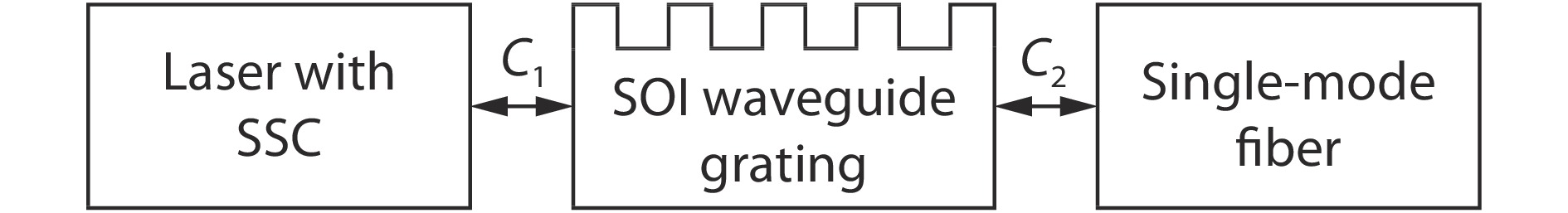
Processing math: 100%
J. Semicond. > 2019, Volume 40 > Issue 10 > 102302

ARTICLES

Simulation of structural design with high coupling efficiency in external cavity semiconductor laser

Yangjie Zhang1, 2, Wentao Guo1, , Di Xiong1, 2, Xiaofeng Guo1, Wenyuan Liao1, 2, Haifeng Liu1, 2, Weihua Liu1, 2 and Manqing Tan1, 2,

+ Author Affiliations

 Corresponding author: Wentao Guo, Email: wtguo@semi.ac.cn; Manqing Tan, Email: mqtan@semi.ac.cn

DOI: 10.1088/1674-4926/40/10/102302

PDF

Turn off MathJax

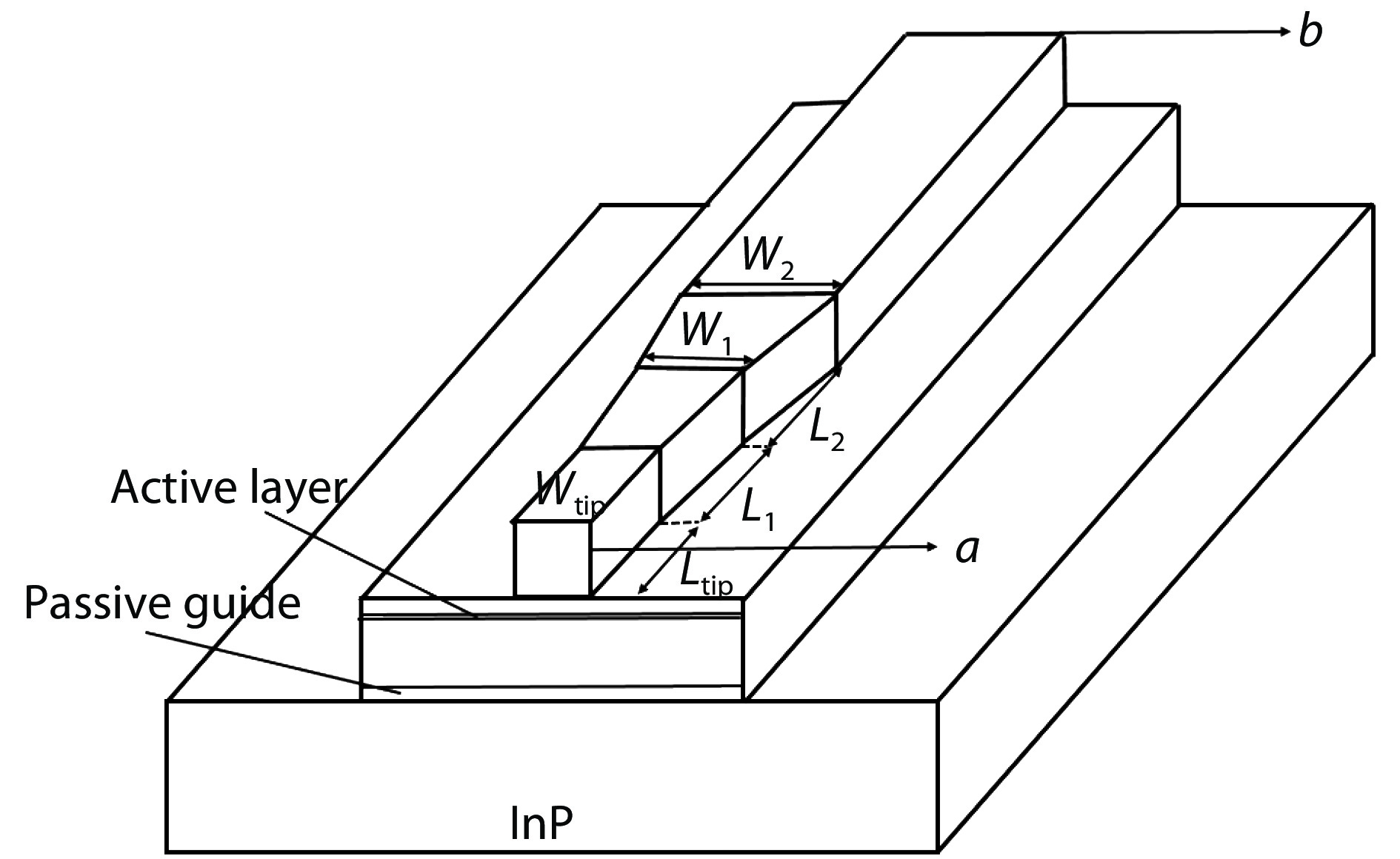
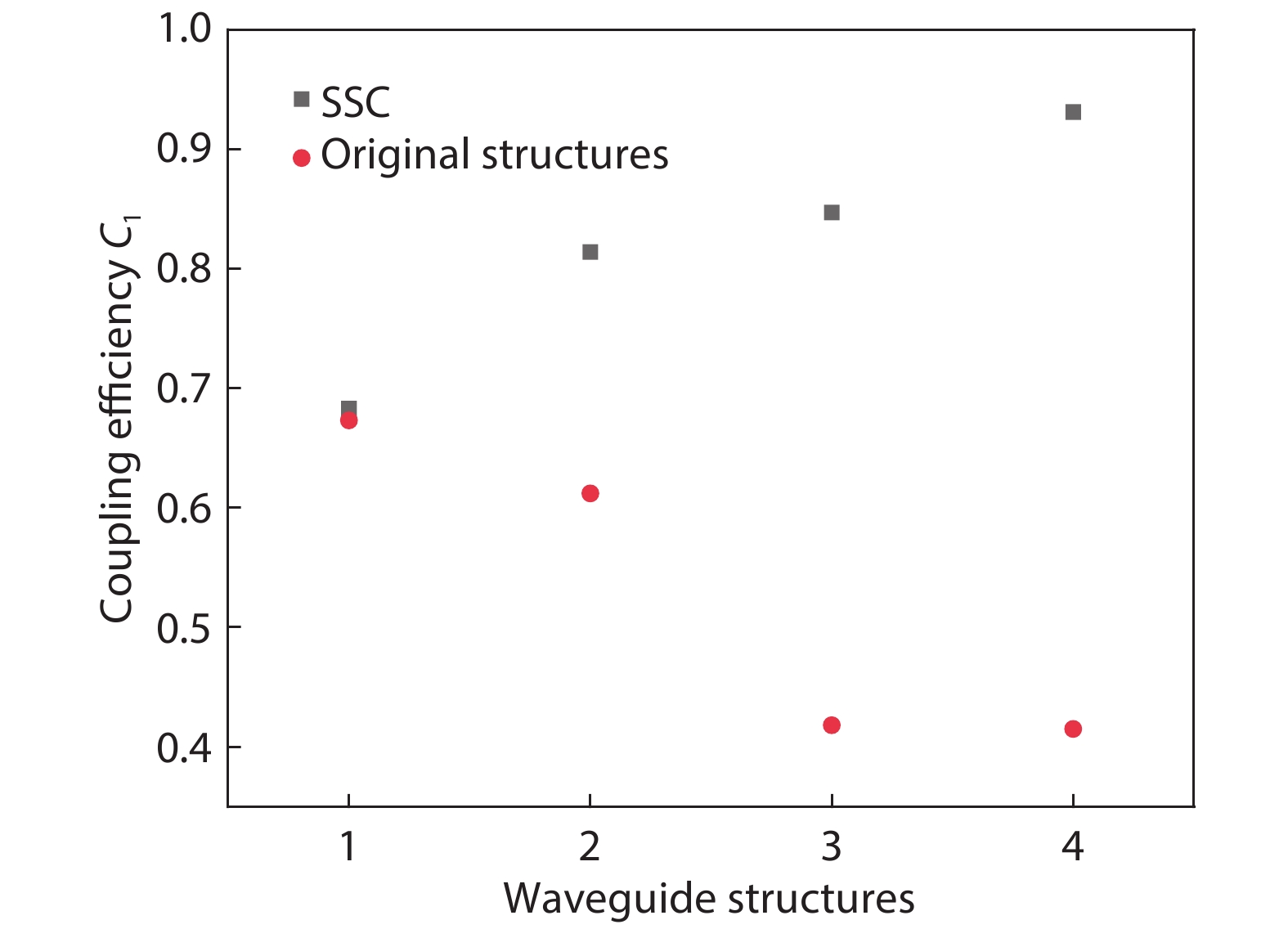
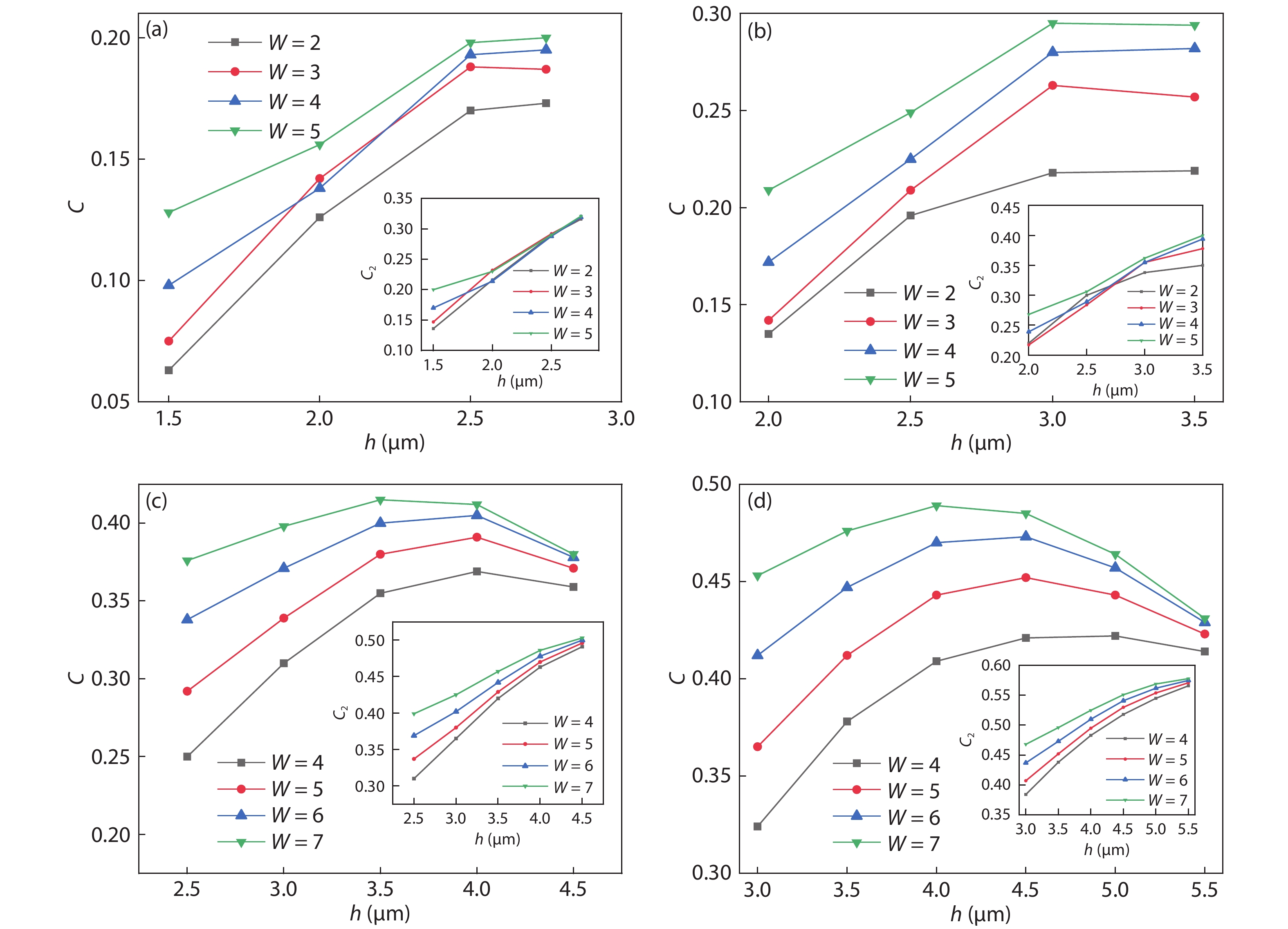
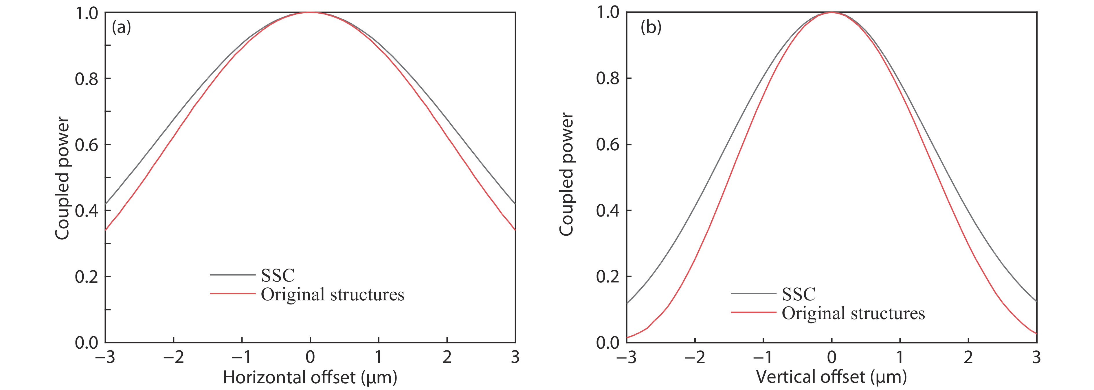
Abstract: For external cavity semiconductor lasers (ECSLs), high coupling efficiency is critical to reducing the linewidth. In this paper, the coupling efficiency between the laser diode and the waveguide grating has been improved, with proposals for its improvement presented, including adding spot-size conversion (SSC) and using a silicon-on-insulator (SOI) waveguide. The results indicate an increase of coupling efficiency from 41.5% to 93.1%, which exhibits an improvement of approximately 51.6% over conventional schemes. The relationship between coupling efficiency and SOI waveguide structures is mainly concerned in this article. These findings provide a new way for the future research of the narrow linewidth of ECSL.

Key words: spot-size conversioncoupling efficiencySOI waveguide

Lasers have been widely used in the field of optical communication and optical sensing, but their application in optical communication and optical sensing is limited owing to the problem of linewidth. ECSL is applied in many fields, such as optical fiber communication, optical storage, optical gyro, coherent detection and so on, due to narrow linewidth, simple structure and convenience for largescale production. In recent years, it has become a research hotspot in the field of international optoelectronic devices[1].

Generally, fiber gratings, waveguide gratings, plane mirrors, etc. are applied for external cavity feedback components of ECSL[2]. Most of the research at home and abroad focuses on fiber gratings and flare gratings[3-5]. The coupling efficiency between the traditional stripe laser structure and the optical fiber is very low. The linewidth of fiber grating external cavity laser is close to several kHz, but it is difficult to achieve precise temperature control. Poor peak wavelength temperature stability and vibration stability possibly cause laser mode hopping.

The expansion of the near-field spot and the improvement of the coupling efficiency are realized by using the SSC. In general, reducing the linewidth of ECSL by improving coupling efficiency has been reported in the research[6-10].

Compared with fiber grating external cavity lasers, waveguide grating external cavity lasesr have better temperature stability and vibration stability[11]. In addition, in order to ensure the high coupling efficiency of ECSL, the optimization of the structure of the SOI ridge waveguide is crucial.

In this paper, the coupling efficiency is calculated in detail, and the condition of single-mode is discussed. Improvement schemes including the structure of SSC and the optimizations of the structure of the SOI ridge waveguide are proposed.

A schematic structure of ECSL is shown in Fig. 1. C1 is the coupling efficiency between laser and SOI waveguide, and C2 is the coupling efficiency between SOI waveguide and single-mode fiber. The coupling efficiency C1 and C2 were calculated by MODE Solution, which is a powerful simulation tool for planar waveguide devices. The total coupling efficiency C (C = C1 × C2) of the corresponding SOI waveguide structures are obtained.

Figure  1.  Schematic structure of ECSL.

Up to now, most SSCs were based on a buried structure with or without selective area growth. Narrow waveguides (below 0.5 μm) are used in many of these structures, which require special lithography and may be sensitive to the width of the taper tip. Recently, a new structure using resonant coupling has been presented theoretically[12], which is a traditional ridge waveguide structure in a single epitaxial and traditional lithography[13]. A schematic of the waveguide structure is shown in Fig. 2. The laser light in the active layer is guided by a narrow 3 μm wide ridge which is gradually tapered down to typically 0.5 μm.

Figure  2.  Schematic of the spot-size converter based on ridge waveguides.

The fundamental transverse electric (TE) mode of the SSC is simulated by software[14]. By optimizing the parameter of Ltip, Wtip, L1, W1, L2, W2, etc. (Ltip is the length of the front rectangular segment, while Wtip is the width of the front rectangular segment. L1 is the length of the first taper and W1 is the width of the first taper; L2 is the length of the second taper, and W2 is the width of the second taper), the mode is squeezed out of the ridge and coupled to the thin passive guide located below the active layer, as is shown in Fig. 3. Fig. 3(a) is the output of TE mode, and Fig. 3(b) is the input of TE mode. The structural parameters in Fig. 2 are determined by simulating (Ltip = 100 μm, Wtip = 0.5 μm, L1 = 300 μm, W1 = 1.4 μm, L2 = 80 μm, W2 = 3 μm). In particular, the mode is guided by a broad ridge, which gradually narrows, and the small spot size of the elliptical shape of the semiconductor laser is converted to a large spot size close to a circle.

Figure  3.  (Color online) Fundamental TE mode at the both facets of the SSC. (a) Output of TE mode at section a in Fig. 2. (b) Input of TE mode at section b in Fig. 2.

MODE solution calculates the power coupling between the modes recorded by two monitors. Overlap measures the fraction of electromagnetic fields that overlap between the two modes. This is also the fraction of power from mode 2 that can propagate in mode 1 (mode 1 and mode 2 are the fundamental modes of two different waveguide structures). The overlap function is being used to estimate the efficiency C1 and C2 between the two waveguides. The overlap can be modeled as

overlap=|Re[(E1×H2dS)(E2×H1dS)E1×H1S]×1Re(E2×H2dS)|,

(1)

where E1, H1 is the electric and magnetic field of mode 1; E2, H2 is the electric and magnetic field of mode 2.

Four waveguide structures are selected to calculate the coupling efficiency C1 with or without SSC. Actually, these four waveguide structures are the structures with the highest total coupling efficiency when H = 3, 4, 5, and 6 μm, respectively. Structure 1: H = 3 μm, h = 2.5 μm, W = 5 μm; Structure 2: H = 4 μm, h = 3 μm, W = 5 μm; Structure 3: H = 5 μm, h = 4 μm, W = 7 μm; Structure 4: H = 6 μm, h = 4 μm, W = 7 μm. H is the height of the inner ridge, h is the height of the outer ridge, and W is the width of the ridge. The coupling efficiency C1 under different waveguide structures is shown in Fig. 4.

Figure  4.  (Color online) Coupling efficiency under different waveguide structures (Structure 1: H = 3 μm, h = 2.5 μm, W = 5 μm; Structure 2: H = 4 μm, h = 3 μm, W = 5 μm; Structure 3: H = 5 μm, h = 4 μm, W = 7 μm; Structure 4: H = 6 μm, h = 4 μm, W = 7 μm).

As can be seen from Fig. 4, the coupling efficiency C1 is greatly improved compared with the original structure without SSC except structure 1. SSC can transform the elliptical spot size of the semiconductor laser into a larger one that is close to the circular one. In addition, since the near-field spot size of the laser output end face becomes larger, the power density of the laser output surface is lowered, which effectively reduces the catastrophic damage of the laser and improves the reliability of the laser. With this method, the coupling efficiency C1 of structure 4 is increased to 93.1%, from 41.5% that of the original structure without SSC.

Fig. 5 is a schematic diagram of SOI ridge waveguide structure. n1,n2 and n3 are refractive indexes of each layer. The parameters of the SOI ridge waveguide model used in the analysis as follows. n1 = 3.5 and n2 = n3 = 1.45; fiber diameter is 8.7 μm; core index is 1.4516; cladding index is 1.4473.

Figure  5.  Schematic diagram of SOI ridge waveguide structure.

In this section, the coupling efficiencies C1 and C2 of different waveguide structures are respectively calculated to obtain the total coupling efficiency C, as shown in Figs. 6(a), 6(b), 6(c) and 6(d), respectively.

Figure  6.  (Color online) Total coupling efficiency C of different SOI waveguide structures. (a) H = 3 μm. (b) H = 4 μm. (c) H = 5 μm. (d) H = 6 μm.

The single mode condition of the waveguide structure is not considered in the above figure, so the subsequent analysis is combined with the single mode cutoff condition. Soref[15, 16] et al.'s research results have indicated that a single-mode SOI waveguide with a large cross-section can be realized as long as the waveguide structure parameters satisfy the single-mode condition:

t0.3+r1r2,r>0.5,

(2)

where t = W/H, r = h/H. Therefore, the size of waveguide section is equivalent to the size of the fiber core layer, which can greatly reduce the coupling loss between waveguide and fiber.

According to the single mode condition, the critical ridge width W is theoretically calculated successively at H = 3, 4, 5, and 6 μm. Under the premise of satisfying the single mode condition, it can be seen from Fig. 6 (a) that the structure with H = 3 μm, h = 2.5 μm and W = 5 μm has the maximum total coupling efficiency, but it is still only 19.8%. The result in Fig. 6(b) confirms that the maximum total coupling efficiency (C) occurs at structure 2 (H = 4 μm, h = 3 μm, W = 5 μm), which is increased to 29.5%. The structure 3 (H = 5 μm, h = 4 μm, W = 7 μm) and structure 4 (H = 6 μm, h = 4 μm, W = 7 μm) corresponding to the maximum C are 41.2% and 48.9%, respectively. Thus, by increasing the height of the outer ridge h, the coupling efficiency between the waveguide and the optical fiber can be improved, since the mode field shape of the SOI waveguide is closer to the mode field shape of the optical fiber. However, at the same time, its overlapping mode field with the SSC is reduced. The optimum point can be determined by the above figures, which is the maximum value at a certain point in the middle of the change of the height h of the outer ridge. The total coupling efficiency of structure 4 is 48.9%. After this, the grating structure which was designed by software can be etched on the SOI waveguide.

By increasing the C0, the linewidth reduces significantly[6], as shown in Fig. 7, where C0 is the coupling coefficient and Iinj is the injection current. On the one hand, the threshold current and threshold carrier density decreased with increasing equivalent reflectance; on the other hand, the strong external cavity feedback makes the mode gain larger.

Figure  7.  (Color online) Effect of coupling coefficient on linewidth characteristics of laser.

Alignment tolerance is a critical aspect that has to be considered in the packaging[17-19]. Fig. 8 shows the normalized coupling efficiencies between SSC and SOI waveguide when both lateral and vertical misalignments of the SOI waveguide are considered. The 50% lateral tolerances of the SOI waveguide are ±1.8 and ±2.7 μm in vertical and horizontal directions, respectively, that meet the requirements in the actual packaging. Compared with the traditional structure, the alignment tolerance is improved by increasing the SSC structure. The tolerance in vertical direction is tighter than that of the horizontal direction, which is most critical in packaging.

Figure  8.  (Color online) Normalized coupling power varied with the offset. (a) Vertical directions. (b) Horizontal directions (SOI waveguide of structure 4: H = 6 μm, h = 4 μm, W = 7 μm).

Aiming at the problems of poor spot quality, low coupling efficiency and poor stability of vibration in the waveguide grating external cavity laser, two improvement schemes are proposed. The experimental results verify the effectiveness of the new approaches investigated in this paper, which can effectively improve the coupling efficiency. In addition, we propose a scheme of SSC to optimize coupling efficiency. SOI ridge waveguide is adopted for the stability of wavelength temperature and vibration to ameliorate. The waveguide structure with the highest coupling efficiency has been determined. According to simulated results, the proposed methodology illustrated 51.6% improvement in coupling efficiency over conventional schemes.


[1]
Lu B, Wei F, Zhang Z, et al. Research on tunable local laser used in ground-to-satellite coherent laser communication. Chin Opt Lett, 2015, 13(9), 091402 doi: 10.3788/COL201513.091402
[2]
Mroziewicz B. External cavity wavelength tunable semiconductor lasers-a review. Opto-Electron Rev, 2008, 16(4), 347 doi: 10.2478/s11772-008-0045-9
[3]
Konosuke A, Shuhei K, Masashi W, et al. Stable and narrow linewidth semiconductor laser assembly with coherent optical negative feedback. Conference on Lasers and Electro-Optics, OSA Technical Digest, 2017
[4]
Liu B, Tong X, Jiang C Y, et al. Development of stable, narrow spectral line-width, fiber delivered laser source for spin exchange optical pumping. Appl Opt, 2015, 54(17), 5420 doi: 10.1364/AO.54.005420
[5]
Fang W, Fei Y, Zhang X, et al. Subkilohertz linewidth reduction of a DFB diode laser using self-injection locking with a fiber Bragg grating Fabry-Perot cavity. Opt Express, 2016, 24(15), 17406 doi: 10.1364/OE.24.017406
[6]
Hisham H K, Mahdiraji G A, Abas A F, et al. Linewidth optimization in fiber grating Fabry-Perot laser. Opt Eng, 2014, 53(2), 026107 doi: 10.1117/1.OE.53.2.026107
[7]
Liu D P, Chen C, Qin L, et al. Study on linewidth characteristics of fiber grating external cavity semiconductor laser. Semicond Optoelectron, 2016, 37(2), 165
[8]
Henry C H. Theory of the linewidth of semiconductor lasers. IEEE J Quantum Electron, 1982, 18(2), 259 doi: 10.1109/JQE.1982.1071522
[9]
Chai Y J, Zhang H Y, Zhou B K. Line width performance and lysis of semiconductor lasers with strong feed back external cavity. Chin J Semicond, 1995, 16(12), 885
[10]
Pan B W, Yu L Q, Lu D, et al. 20 kHz narrow linewidth fiber Bragg grating external cavity semiconductor laser. Chin J Lasers, 2015, 42(05), 49 doi: 10.3788/CJL201542.0502007
[11]
Alalusi M, Brasil P, Lee S, et al. Low noise planar external cavity laser for interferometric fiber optic sensors. Proc SPIE, 2009, 7316
[12]
Vusirikala V, Saini S S, Bartolo R E, et al. Compact mode expanders using resonant coupling between a tapered active region and an underlying coupling waveguide. IEEE Photonics Technol Lett, 1998, 10(2), 203 doi: 10.1109/68.655358
[13]
Bissessur H, Graver C, Gouezigou O L, et al. Ridge laser with spot-size converter in a single epitaxial step for high coupling efficiency to single-mode fibers. IEEE Photonics Technol Lett, 1998, 10(9), 1235 doi: 10.1109/68.705601
[14]
Tsuchizawa T, Watanabe T, Yamada K, et al. Microphotonics devices based on silicon microfabrication technology. IEEE J Sel Top Quantum Electron, 2005, 11(1), 232 doi: 10.1109/JSTQE.2004.841479
[15]
Soref R A, Schmidthen J, Petermann K. Large single-mode rib waveguide in GeSi and Si-on-SiO2. IEEE J Quantum Electron, 1991, 27(8), 1971 doi: 10.1109/3.83406
[16]
Richman A G, Ree G T, Namavar F. Silicon-on-insulator optical rib waveguide loss and mode characteristics. J Lightwave Technol, 1994, 12(10), 1771 doi: 10.1109/50.337489
[17]
Sumy M, Steffen S, Ralf S, et al. Geometrical tolerance of optical fiber and laser diode for passive alignment using LTCC technology. German Microwave Conference, 2015, 363 doi: 10.1109/GEMIC.2015.7107828
[18]
Romero-Garcia S, Marzban B, Merget F, et al. Edge Couplers with relaxed alignment tolerance for pick-and-place hybrid integration of III–V lasers with SOI waveguides. IEEE J Sel Top Quantum Electron, 2014, 20(4), 369 doi: 10.1109/JSTQE.2013.2292523
[19]
Shen P K, Chen C T, Chang C H, et al. Implementation of chip-level optical interconnect with laser and photodetector using SOI-based 3-D guided-wave path. IEEE Photonics J, 2014, 6(6), 1 doi: 10.1109/JPHOT.2014.2366165
Fig. 1.  Schematic structure of ECSL.

Fig. 2.  Schematic of the spot-size converter based on ridge waveguides.

Fig. 3.  (Color online) Fundamental TE mode at the both facets of the SSC. (a) Output of TE mode at section a in Fig. 2. (b) Input of TE mode at section b in Fig. 2.

Fig. 4.  (Color online) Coupling efficiency under different waveguide structures (Structure 1: H = 3 μm, h = 2.5 μm, W = 5 μm; Structure 2: H = 4 μm, h = 3 μm, W = 5 μm; Structure 3: H = 5 μm, h = 4 μm, W = 7 μm; Structure 4: H = 6 μm, h = 4 μm, W = 7 μm).

Fig. 5.  Schematic diagram of SOI ridge waveguide structure.

Fig. 6.  (Color online) Total coupling efficiency C of different SOI waveguide structures. (a) H = 3 μm. (b) H = 4 μm. (c) H = 5 μm. (d) H = 6 μm.

Fig. 7.  (Color online) Effect of coupling coefficient on linewidth characteristics of laser.

Fig. 8.  (Color online) Normalized coupling power varied with the offset. (a) Vertical directions. (b) Horizontal directions (SOI waveguide of structure 4: H = 6 μm, h = 4 μm, W = 7 μm).

[1]
Lu B, Wei F, Zhang Z, et al. Research on tunable local laser used in ground-to-satellite coherent laser communication. Chin Opt Lett, 2015, 13(9), 091402 doi: 10.3788/COL201513.091402
[2]
Mroziewicz B. External cavity wavelength tunable semiconductor lasers-a review. Opto-Electron Rev, 2008, 16(4), 347 doi: 10.2478/s11772-008-0045-9
[3]
Konosuke A, Shuhei K, Masashi W, et al. Stable and narrow linewidth semiconductor laser assembly with coherent optical negative feedback. Conference on Lasers and Electro-Optics, OSA Technical Digest, 2017
[4]
Liu B, Tong X, Jiang C Y, et al. Development of stable, narrow spectral line-width, fiber delivered laser source for spin exchange optical pumping. Appl Opt, 2015, 54(17), 5420 doi: 10.1364/AO.54.005420
[5]
Fang W, Fei Y, Zhang X, et al. Subkilohertz linewidth reduction of a DFB diode laser using self-injection locking with a fiber Bragg grating Fabry-Perot cavity. Opt Express, 2016, 24(15), 17406 doi: 10.1364/OE.24.017406
[6]
Hisham H K, Mahdiraji G A, Abas A F, et al. Linewidth optimization in fiber grating Fabry-Perot laser. Opt Eng, 2014, 53(2), 026107 doi: 10.1117/1.OE.53.2.026107
[7]
Liu D P, Chen C, Qin L, et al. Study on linewidth characteristics of fiber grating external cavity semiconductor laser. Semicond Optoelectron, 2016, 37(2), 165
[8]
Henry C H. Theory of the linewidth of semiconductor lasers. IEEE J Quantum Electron, 1982, 18(2), 259 doi: 10.1109/JQE.1982.1071522
[9]
Chai Y J, Zhang H Y, Zhou B K. Line width performance and lysis of semiconductor lasers with strong feed back external cavity. Chin J Semicond, 1995, 16(12), 885
[10]
Pan B W, Yu L Q, Lu D, et al. 20 kHz narrow linewidth fiber Bragg grating external cavity semiconductor laser. Chin J Lasers, 2015, 42(05), 49 doi: 10.3788/CJL201542.0502007
[11]
Alalusi M, Brasil P, Lee S, et al. Low noise planar external cavity laser for interferometric fiber optic sensors. Proc SPIE, 2009, 7316
[12]
Vusirikala V, Saini S S, Bartolo R E, et al. Compact mode expanders using resonant coupling between a tapered active region and an underlying coupling waveguide. IEEE Photonics Technol Lett, 1998, 10(2), 203 doi: 10.1109/68.655358
[13]
Bissessur H, Graver C, Gouezigou O L, et al. Ridge laser with spot-size converter in a single epitaxial step for high coupling efficiency to single-mode fibers. IEEE Photonics Technol Lett, 1998, 10(9), 1235 doi: 10.1109/68.705601
[14]
Tsuchizawa T, Watanabe T, Yamada K, et al. Microphotonics devices based on silicon microfabrication technology. IEEE J Sel Top Quantum Electron, 2005, 11(1), 232 doi: 10.1109/JSTQE.2004.841479
[15]
Soref R A, Schmidthen J, Petermann K. Large single-mode rib waveguide in GeSi and Si-on-SiO2. IEEE J Quantum Electron, 1991, 27(8), 1971 doi: 10.1109/3.83406
[16]
Richman A G, Ree G T, Namavar F. Silicon-on-insulator optical rib waveguide loss and mode characteristics. J Lightwave Technol, 1994, 12(10), 1771 doi: 10.1109/50.337489
[17]
Sumy M, Steffen S, Ralf S, et al. Geometrical tolerance of optical fiber and laser diode for passive alignment using LTCC technology. German Microwave Conference, 2015, 363 doi: 10.1109/GEMIC.2015.7107828
[18]
Romero-Garcia S, Marzban B, Merget F, et al. Edge Couplers with relaxed alignment tolerance for pick-and-place hybrid integration of III–V lasers with SOI waveguides. IEEE J Sel Top Quantum Electron, 2014, 20(4), 369 doi: 10.1109/JSTQE.2013.2292523
[19]
Shen P K, Chen C T, Chang C H, et al. Implementation of chip-level optical interconnect with laser and photodetector using SOI-based 3-D guided-wave path. IEEE Photonics J, 2014, 6(6), 1 doi: 10.1109/JPHOT.2014.2366165
1

Cross-dimensional electron–phonon coupling

Jun Zhang

Journal of Semiconductors, 2019, 40(9): 090201. doi: 10.1088/1674-4926/40/9/090201

2

Simulation and application of external quantum efficiency of solar cells based on spectroscopy

Guanlin Chen, Can Han, Lingling Yan, Yuelong Li, Ying Zhao, et al.

Journal of Semiconductors, 2019, 40(12): 122701. doi: 10.1088/1674-4926/40/12/122701

3

A high-efficiency grating coupler between single-mode fiber and silicon-on-insulator waveguide

Rongrui Liu, Yubing Wang, Dongdong Yin, Han Ye, Xiaohong Yang, et al.

Journal of Semiconductors, 2017, 38(5): 054007. doi: 10.1088/1674-4926/38/5/054007

4

Electro-magnetic weak coupling optical polaron and temperature effect in quantum dot

M. Tiotsop, A. J. Fotue, S. C. Kenfack, N. Issofa, A. V. Wirngo, et al.

Journal of Semiconductors, 2015, 36(10): 102001. doi: 10.1088/1674-4926/36/10/102001

5

Tunable filters based on an SOI nano-wire waveguide micro ring resonator

Li Shuai, Wu Yuanda, Yin Xiaojie, An Junming, Li Jianguang, et al.

Journal of Semiconductors, 2011, 32(8): 084007. doi: 10.1088/1674-4926/32/8/084007

6

Analysis of the thermo-optic effect in lateral-carrier-injection SOI ridge waveguide devices

Zhao Jiate, Zhao Yong, Wang Wanjun, Hao Yinlei, Zhou Qiang, et al.

Journal of Semiconductors, 2010, 31(6): 064009. doi: 10.1088/1674-4926/31/6/064009

7

Photoelectric conversion characteristics of ZnO/SiC/Si heterojunctions

Wu Xiaopeng, Chen Xiaoqing, Sun Lijie, Mao Shun, Fu Zhuxi, et al.

Journal of Semiconductors, 2010, 31(10): 103002. doi: 10.1088/1674-4926/31/10/103002

8

A high efficiency charge pump circuit for low power applications

Feng Peng, Li Yunlong, Wu Nanjian

Journal of Semiconductors, 2010, 31(1): 015009. doi: 10.1088/1674-4926/31/1/015009

9

A Single Fiber Coupling Technique for High Power Diode Laser Arrays

Niu Gang, Fan Zhongwei, Wang Peifeng, Cui Jianfeng, Shi Zhaohui, et al.

Chinese Journal of Semiconductors , 2007, 28(10): 1607-1610.

10

An Implementation of a CMOS Down-Conversion Mixer for GSM1900 Receivers

Chu Fangqing, Li Wei, Su Yanfeng, Ren Junyan

Chinese Journal of Semiconductors , 2006, 27(3): 467-472.

11

Low-Microwave Loss Coplanar Waveguides Fabricated on High-Resistivity Silicon Substrate

Yang Hua, Zhu Hongliang, Xie Hongyun, Zhao Lingjuan, Zhou Fan, et al.

Chinese Journal of Semiconductors , 2006, 27(1): 1-4.

12

An Analytical Expression of Free Carrier Lifetime in an SOI Rib Waveguide Used for Raman Amplification

Chen Mingyi, Mao Luhong, Hao Xianren, Zhang Shilin, Guo Weilian, et al.

Chinese Journal of Semiconductors , 2006, 27(7): 1310-1315.

13

An Evanescent Coupling Approach for Optical Characterization of ZnO Nanowires

Yang Qing, Lou Jingyi, Yang Deren, Tong Limin

Chinese Journal of Semiconductors , 2006, 27(3): 425-428.

14

Recent Progress on SOI-Based High-Speed Electro-Optic Modulators

Huang Qingzhong, Yu Jinzhong

Chinese Journal of Semiconductors , 2006, 27(12): 2069-2074.

15

Analysis of Coupling Efficiency of TO-Packaged VCSELs

Liu Chao, Wang Xin, Yuan Haiqing, Zhong Baoxuan, Zhu Ninghua, et al.

Chinese Journal of Semiconductors , 2006, 27(4): 751-755.

16

Optimization Design of Superluminescent Diodes with RWGStructure for High Efficiency Coupling with SMFs

Zhong Xin, Huang Yidong, Zhao Han, Zhang Wei, Peng Jiangde, et al.

Chinese Journal of Semiconductors , 2006, 27(4): 683-687.

17

Monolithically Integrated Laser Diode and Electroabsorption Modulator with Dual- Waveguide Spot-Size Converter Output

Chinese Journal of Semiconductors , 2005, 26(6): 1094-1099.

18

An Electroabsorption Modulator Monolithically Integrated with a Semiconductor Optical Amplifier and a Dual-Waveguide Spot-Size Converter

Chinese Journal of Semiconductors , 2005, 26(8): 1504-1508.

19

An Efficient MMI SOI Splitter with Multimode Input/Output Waveguides

Fang Qing, He Yuejiao, Xin Hongli, Li Fang,and Liu Yuliang

Chinese Journal of Semiconductors , 2005, 26(2): 276-280.

20

1.55μm Laser Diode Monolithically Integrated with Spot-Size Converter Using Conventional Process

Hou Lianping, Wang Wei, and Zhu Hongliang

Chinese Journal of Semiconductors , 2005, 26(3): 443-447.

  • Search

    Advanced Search >>

    GET CITATION

    Yangjie Zhang, Wentao Guo, Di Xiong, Xiaofeng Guo, Wenyuan Liao, Haifeng Liu, Weihua Liu, Manqing Tan. Simulation of structural design with high coupling efficiency in external cavity semiconductor laser[J]. Journal of Semiconductors, 2019, 40(10): 102302. doi: 10.1088/1674-4926/40/10/102302
    Y J Zhang, W T Guo, D Xiong, X F Guo, W Y Liao, H F Liu, W H Liu, M Q Tan, Simulation of structural design with high coupling efficiency in external cavity semiconductor laser[J]. J. Semicond., 2019, 40(10): 102302. doi: 10.1088/1674-4926/40/10/102302.
    shu

    Export: BibTex EndNote

    Article Metrics

    Article views: 3527 Times PDF downloads: 72 Times Cited by: 0 Times

    History

    Received: 01 July 2019 Revised: 16 August 2019 Online: Accepted Manuscript: 10 September 2019Uncorrected proof: 11 September 2019Published: 01 October 2019

    Catalog

      Email This Article

      User name:
      Email:*请输入正确邮箱
      Code:*验证码错误
      Yangjie Zhang, Wentao Guo, Di Xiong, Xiaofeng Guo, Wenyuan Liao, Haifeng Liu, Weihua Liu, Manqing Tan. Simulation of structural design with high coupling efficiency in external cavity semiconductor laser[J]. Journal of Semiconductors, 2019, 40(10): 102302. doi: 10.1088/1674-4926/40/10/102302 ****Y J Zhang, W T Guo, D Xiong, X F Guo, W Y Liao, H F Liu, W H Liu, M Q Tan, Simulation of structural design with high coupling efficiency in external cavity semiconductor laser[J]. J. Semicond., 2019, 40(10): 102302. doi: 10.1088/1674-4926/40/10/102302.
      Citation:
      Yangjie Zhang, Wentao Guo, Di Xiong, Xiaofeng Guo, Wenyuan Liao, Haifeng Liu, Weihua Liu, Manqing Tan. Simulation of structural design with high coupling efficiency in external cavity semiconductor laser[J]. Journal of Semiconductors, 2019, 40(10): 102302. doi: 10.1088/1674-4926/40/10/102302 ****
      Y J Zhang, W T Guo, D Xiong, X F Guo, W Y Liao, H F Liu, W H Liu, M Q Tan, Simulation of structural design with high coupling efficiency in external cavity semiconductor laser[J]. J. Semicond., 2019, 40(10): 102302. doi: 10.1088/1674-4926/40/10/102302.

      Simulation of structural design with high coupling efficiency in external cavity semiconductor laser

      DOI: 10.1088/1674-4926/40/10/102302
      More Information

      Catalog

        /

        DownLoad:  Full-Size Img  PowerPoint
        Return
        Return