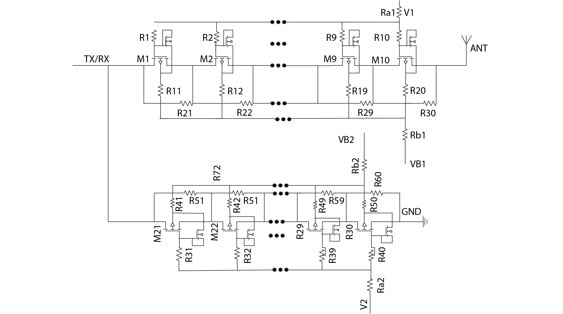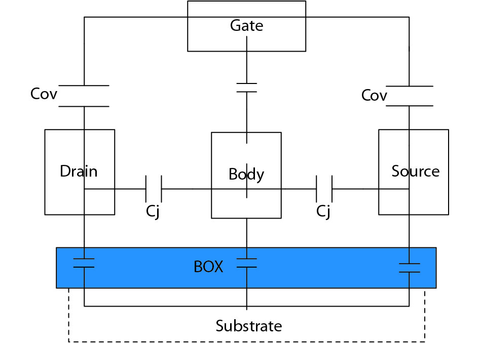
Fig. 1.
(Color online) Simplified capacitive models.
ARTICLES
Hong Guan1, , Hao Sun2, Junlin Bao1, Zhipeng Wang2, Shuguang Zhou2 and Hongwei Zhu2
Corresponding author: Hong Guan, Email: guanhong116@163.com
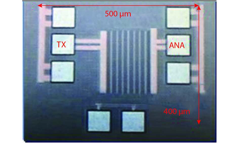
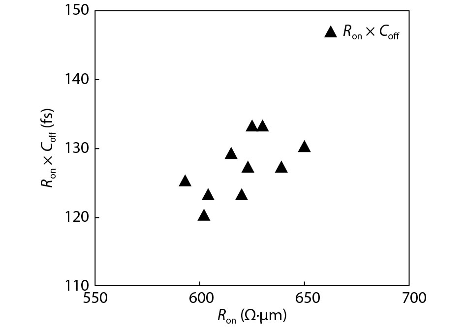
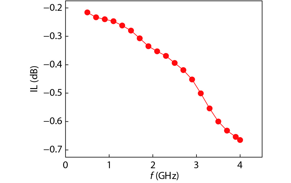
Abstract: A high-performance single-pole single-throw (SPST) RF switch for mobile phone RF front-end modules (FEMs) was designed and characterized in a 0.13 μm partially depleted silicon-on-insulator (PD SOI) process. In this paper, the traditional series-shunt configuration design was improved by introducing a suitably large DC bias resistor and leakage-preventing PMOS, together with the floating body technique. The performance of the RF switch is greatly improved. Furthermore, a new Ron × Coff testing method is also proposed. The size of this SPST RF switch is 0.2 mm2. This switch can be widely used for present 4G and forthcoming 5G mobile phone FEMs.
Keywords: RF switch, SOI, insertion loss, isolation, linearity
| [1] |
C L Chen, P W Wyatt, D R Yost. Fully depleted SOI RF switch with dynamic biasing. IEEE Radio Frequency Integrated Circuits Symposium, 2007: 175 doi: 10.1109/RFIC.2007.380859
|
| [2] |
D Kelly, C Brindle, C Kemerling. The state-of-the-art of silicon-on-sapphire CMOS RF switches. Compound Semiconductor Integrated Circuit Symposium, 2005: 200 doi: 10.1109/CSICS.2005.1531812
|
| [3] |
S Makioka, Y Anda, K Miyatsuji. Super self-aligned GaAs RF switch IC with 0.25 dB extremely low insertion loss for mobile communication systems. IEEE Trans Electron Devices, 2001, 48(8): 1500. doi: 10.1109/16.936499
|
| [4] |
F J Huang, O Kenneth. A 0.5-μm CMOS T/R switch for 900 MHz wireless applications. IEEE J Solid-State Circuit, 2001, 36(3): 486. doi: 10.1109/4.910487
|
| [5] |
F Gianesello, A Momroy, V Vialla. Highly linear and sub 120 fs Ron × Coff 130 nm RF SOI technology targeting 5G carrier aggregation RF switches and FEM SOC. IEEE Silicon Monolithic Integrated Circuits in RF Systems, 2016: 9. doi: 10.1109/SIRF.2016.7445454
|
| [6] |
P A Rabbeni, A Joseph. RF SOI: revolutionizing RF system design. Microwave J, 2015, 58(10): 22.
|
| [7] |
X S Wang, X Wang, F Lu. Concurrent design analysis of high-linearity SP10T switch with 8.5 kV ESD protection. IEEE J Solid-State Circuit, 2014, 49(9): 1927. doi: 10.1109/JSSC.2014.2331956
|
| [8] |
X S Wang, X Wang, F Lu. A smartphone SP10T T/R switch in 180-nm SOI CMOS with 8kV + ESD protection by co-design. Custom Integrated Circuit Conference, 2013: 1 doi: 10.1109/CICC.2013.6658474
|
| [9] |
B K Esfeh, M Rack, S Makovejev. A SPDT RF switch small and large signal characteristics on TR-HR SOI substrates. IEEE J Electron Devices Soc, 2018,(6): 543. doi: 10.1109/JEDS.2018.2805780
|
| [10] |
C Tinella, O Richard, A Cathelin. 0.13μm CMOS SOI SP6T antenna switch for multi-standard handsets. IEEE Silicon Monolithic Integrated Circuits in RF Systems, 2006: 4. doi: 10.1109/SMIC.2005.1587904
|
| [11] |
I Song, M K Cho. PNP-based RF switches for the mitigation of single-event transients in a complementary SiGe BiCMOS platform. IEEE Trans Nucl Sci, 2017, 65(1): 391. doi: 10.1109/TNS.2017.2780120
|
| [12] |
M D Wei, R Negra. High-isolation stacked RF switch using dc-lift and feed forward cancellation techniques in standard 65 nm CMOS. IEEE International Symposium, 2018: 1 doi: 10.1109/ISCAS.2018.8351259
|


Article views: 7472 Times PDF downloads: 320 Times Cited by: 0 Times
Received: 06 June 2018 Revised: 21 September 2018 Online: Accepted Manuscript: 05 November 2018Uncorrected proof: 05 November 2018Published: 01 February 2019
| Citation: |
Hong Guan, Hao Sun, Junlin Bao, Zhipeng Wang, Shuguang Zhou, Hongwei Zhu. High-performance RF Switch in 0.13 μm RF SOI process[J]. Journal of Semiconductors, 2019, 40(2): 022401. doi: 10.1088/1674-4926/40/2/022401
****
H Guan, H Sun, J L Bao, Z P Wang, S G Zhou, H W Zhu, High-performance RF Switch in 0.13 μm RF SOI process[J]. J. Semicond., 2019, 40(2): 022401. doi: 10.1088/1674-4926/40/2/022401.

|
| [1] |
C L Chen, P W Wyatt, D R Yost. Fully depleted SOI RF switch with dynamic biasing. IEEE Radio Frequency Integrated Circuits Symposium, 2007: 175 doi: 10.1109/RFIC.2007.380859
|
| [2] |
D Kelly, C Brindle, C Kemerling. The state-of-the-art of silicon-on-sapphire CMOS RF switches. Compound Semiconductor Integrated Circuit Symposium, 2005: 200 doi: 10.1109/CSICS.2005.1531812
|
| [3] |
S Makioka, Y Anda, K Miyatsuji. Super self-aligned GaAs RF switch IC with 0.25 dB extremely low insertion loss for mobile communication systems. IEEE Trans Electron Devices, 2001, 48(8): 1500. doi: 10.1109/16.936499
|
| [4] |
F J Huang, O Kenneth. A 0.5-μm CMOS T/R switch for 900 MHz wireless applications. IEEE J Solid-State Circuit, 2001, 36(3): 486. doi: 10.1109/4.910487
|
| [5] |
F Gianesello, A Momroy, V Vialla. Highly linear and sub 120 fs Ron × Coff 130 nm RF SOI technology targeting 5G carrier aggregation RF switches and FEM SOC. IEEE Silicon Monolithic Integrated Circuits in RF Systems, 2016: 9. doi: 10.1109/SIRF.2016.7445454
|
| [6] |
P A Rabbeni, A Joseph. RF SOI: revolutionizing RF system design. Microwave J, 2015, 58(10): 22.
|
| [7] |
X S Wang, X Wang, F Lu. Concurrent design analysis of high-linearity SP10T switch with 8.5 kV ESD protection. IEEE J Solid-State Circuit, 2014, 49(9): 1927. doi: 10.1109/JSSC.2014.2331956
|
| [8] |
X S Wang, X Wang, F Lu. A smartphone SP10T T/R switch in 180-nm SOI CMOS with 8kV + ESD protection by co-design. Custom Integrated Circuit Conference, 2013: 1 doi: 10.1109/CICC.2013.6658474
|
| [9] |
B K Esfeh, M Rack, S Makovejev. A SPDT RF switch small and large signal characteristics on TR-HR SOI substrates. IEEE J Electron Devices Soc, 2018,(6): 543. doi: 10.1109/JEDS.2018.2805780
|
| [10] |
C Tinella, O Richard, A Cathelin. 0.13μm CMOS SOI SP6T antenna switch for multi-standard handsets. IEEE Silicon Monolithic Integrated Circuits in RF Systems, 2006: 4. doi: 10.1109/SMIC.2005.1587904
|
| [11] |
I Song, M K Cho. PNP-based RF switches for the mitigation of single-event transients in a complementary SiGe BiCMOS platform. IEEE Trans Nucl Sci, 2017, 65(1): 391. doi: 10.1109/TNS.2017.2780120
|
| [12] |
M D Wei, R Negra. High-isolation stacked RF switch using dc-lift and feed forward cancellation techniques in standard 65 nm CMOS. IEEE International Symposium, 2018: 1 doi: 10.1109/ISCAS.2018.8351259
|

 WeChat ID
Journal of Semiconductors © 2017 All Rights Reserved 京ICP备05085259号-2

 DownLoad: