


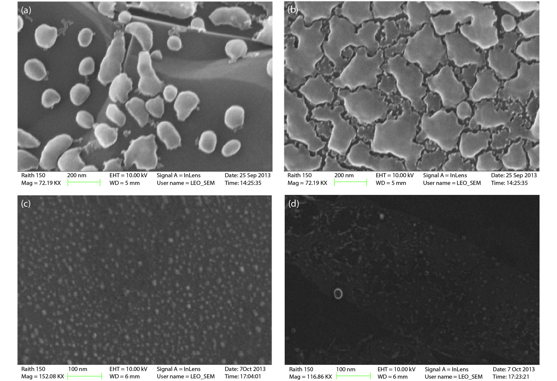
Fig. 1.
SEM images of epitaxial silicon grown on graphite substrates. (a) and (b) from two areas on S1; (c) and (d) from two areas on S2.
ARTICLES
Naili Yue1, Joshua Myers2, Liqin Su1, Wentao Wang3, Fude Liu3, Raphael Tsu1, Yan Zhuang2 and Yong Zhang1,
Corresponding author: Yong Zhang, E-mail: Yong.Zhang@uncc.edu
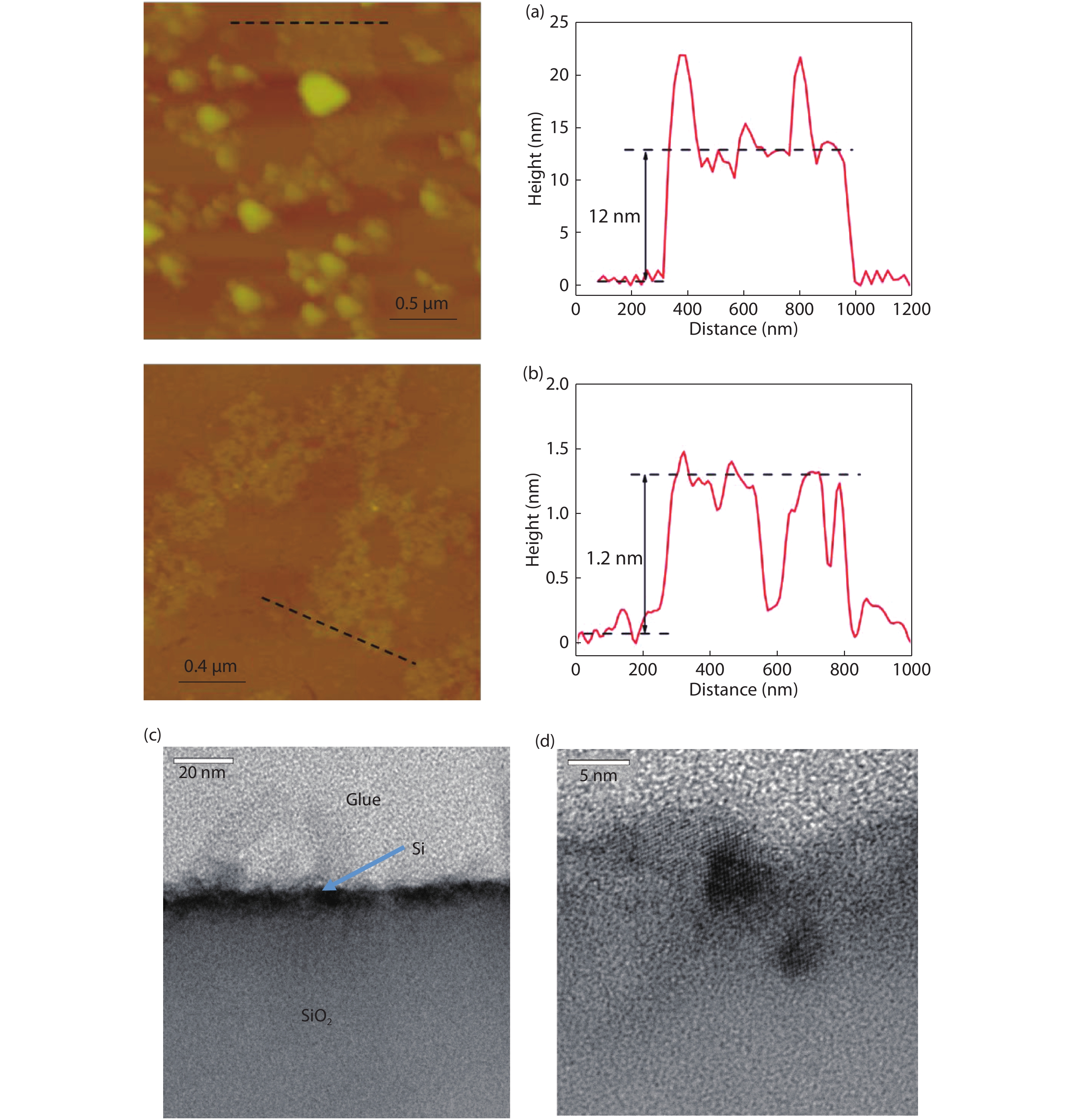
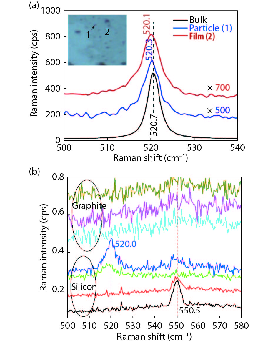
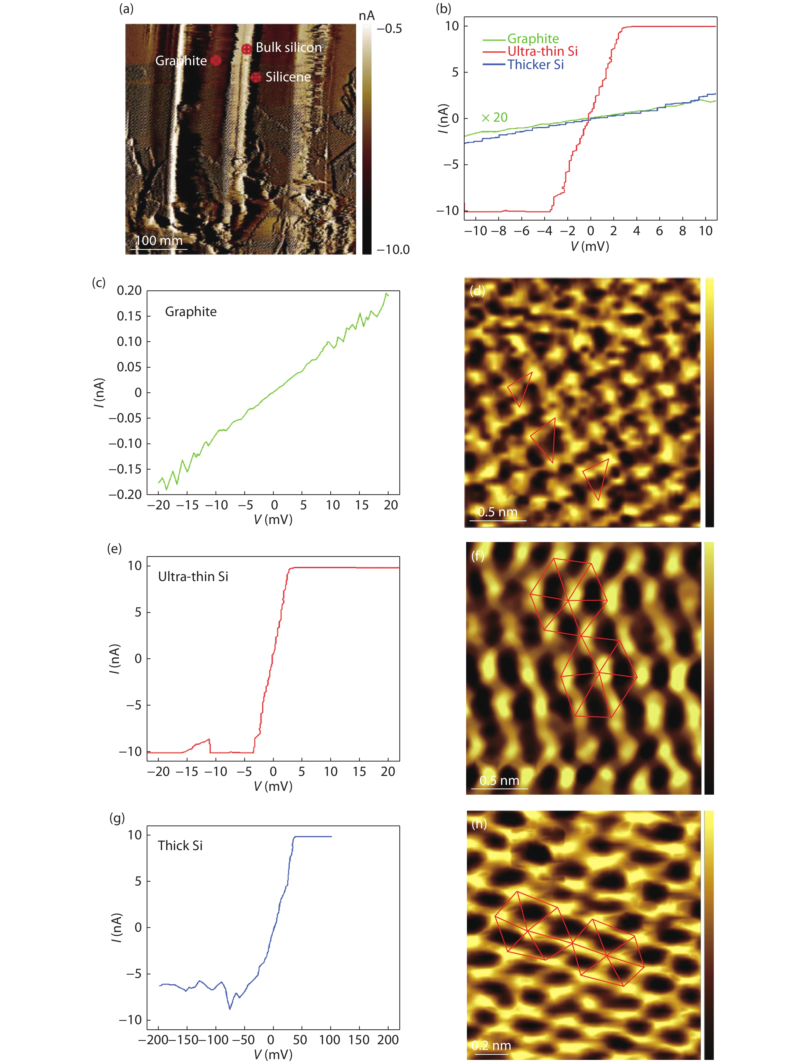
Abstract: We report the growth of Si nanostructures, either as thin films or nanoparticles, on graphene substrates. The Si nanostructures are shown to be single crystalline, air stable and oxidation resistive, as indicated by the observation of a single crystalline Si Raman mode at around 520 cm–1, a STM image of an ordered surface structure under ambient condition, and a Schottky junction with graphite. Ultra-thin silicon regions exhibit silicene-like behavior, including a Raman mode at around 550 cm–1, a triangular lattice structure in STM that has distinctly different lattice spacing from that of either graphene or thicker Si, and metallic conductivity of up to 500 times higher than that of graphite. This work suggests a bottom-up approach to forming a Si nanostructure array on a large-scale patterned graphene substrate that can be used to fabricate nanoscale Si electronic devices.
Keywords: silicene, silicon, Raman, STM, epitaxial growth, oxidation
| [1] |
Guzm-Verri G G, Lew Yan Voon L C. Electronic structure of silicon-based nanostructures. Phys Rev B, 2007, 76, 075131 doi: 10.1103/PhysRevB.76.075131
|
| [2] |
Vogt P, De Padova P, Quaresima C, et al. Silicene: compelling experimental evidence for graphenelike two-dimensional silicon. Phys Rev Lett, 2012, 108, 155501 doi: 10.1103/PhysRevLett.108.155501
|
| [3] |
Fleurence A, Friedlein R, Ozaki T, et al. Experimental evidence for epitaxial silicene on diboride thin Films. Phys Rev Lett, 2012, 108, 245501 doi: 10.1103/PhysRevLett.108.245501
|
| [4] |
Cinquanta E, Scalise E., Chiappe D, et al Getting through the nature of silicene: an sp2-sp3 two-dimensional silicon nanosheet. J Phys Chem C, 20113, 117, 16719 doi: 10.1021/jp405642g
|
| [5] |
Yan J A, Stein R, Schaefer D M, et al. Electron-phonon coupling in two-dimensional silicene and germanene. Phys Rev B, 2013, 88, 121403 doi: 10.1103/PhysRevB.88.121403
|
| [6] |
Scalise E, Houssa M, Pourtois G, et al. Vibrational properties of silicene and germanene. Nano Res, 2013, 6, 19 doi: 10.1007/s12274-012-0277-3
|
| [7] |
Solonenko D, Gordan O, Lay G L, et al. 2D vibrational properties of epitaxial silicene on Ag(111). 2D Mater, 2017, 4, 015008 doi: 10.1088/2053-1583/4/1/015008
|
| [8] |
Zhuang J, Xu X, Du Y, et al. Investigation of electron–phonon coupling in epitaxial silicene by in situ Raman spectroscopy. Phys Rev B, 2015, 91, 161409 doi: 10.1103/PhysRevB.91.161409
|
| [9] |
Sheng S, Wu J B, Cong X, et al. Vibrational properties of a monolayer silicene sheet studied by tip-enhanced Raman spectroscopy. Phys Rev Lett, 2017, 119, 196803 doi: 10.1103/PhysRevLett.119.196803
|
| [10] |
Wu J B, Lin M L, Cong X, et al. Raman spectroscopy of graphene-based materials and its applications in related devices. Chem Soc Rev, 2018, 47, 1822 doi: 10.1039/C6CS00915H
|
| [11] |
De Padova P, Ottaviani C, Quaresima C, et al. 24 h stability of thick multilayer silicene in air. 2D Mater, 2014, 1, 021003 doi: 10.1088/2053-1583/1/2/021003
|
| [12] |
Zhang Y, Tsu R. Binding graphene sheets together using silicon: graphene/silicon superlattice. Nanoscale Res Lett, 2010, 5, 805 doi: 10.1007/s11671-010-9561-x
|
| [13] |
Neuendorf R, Palmer R E, Smith R. Low energy deposition of size-selected Si clusters onto graphite. Chem Phys Lett, 2001, 333, 304 doi: 10.1016/S0009-2614(00)01364-6
|
| [14] |
Cai Y, Chuu C P, Wei C M, et al. Stability and electronic properties of two-dimensional silicene and germanene on graphene. Phys Rev B, 2013, 88, 245408 doi: 10.1103/PhysRevB.88.245408
|
| [15] |
Yu S, Li X D, Wu S Q, et al. Novel electronic structures of superlattice composed of graphene and silicene. Mater Res Bull, 2014, 50, 268 doi: 10.1016/j.materresbull.2013.11.033
|
| [16] |
Fahy S, Louie S G, Cohen M L. Pseudopotential total-energy study of the transition from rhombohedral graphite to diamond. Phys Rev B, 1986, 34, 1191 doi: 10.1103/PhysRevB.34.1191
|
| [17] |
Wang J, Zhang Y. Topologic connection between 2-D layered structures and 3-D diamond structures for conventional semiconductors. Sci Rep, 2016, 6, 24660 doi: 10.1038/srep24660
|
| [18] |
Zhang Y, Tsu R, Yue N. Growth of semiconductors on hetero-substrates using graphene as an interfacial layer. US Patent, US2014/039596, 2014
|
| [19] |
De Crescenzi M, Berbezier I, Scarselli M, et al. Formation of silicene nanosheets on graphite. ACS Nano, 2016, 10, 11163 doi: 10.1021/acsnano.6b06198
|
| [20] |
Li Y, Wang H, Xie L, et al. MoS2 nanoparticles grown on graphene: an advanced catalyst for the hydrogen evolution reaction. J Am Cheml Soc, 2011, 133, 7296 doi: 10.1021/ja201269b
|
| [21] |
Ugeda M M, Bradley A J, Shi S F, et al. Giant bandgap renormalization and excitonic effects in a monolayer transition metal dichalcogenide semiconductor. Nat Mater, 2014, 13, 1091 doi: 10.1038/nmat4061
|
| [22] |
Teplin C W, Paranthaman M P, Fanning T R, et al. Heteroepitaxial film crystal silicon on Al2O3: new route to inexpensive crystal silicon photovoltaics. Energy Environ Sci, 2011, 4, 3346 doi: 10.1039/c1ee01555a
|
| [23] |
Zhang K, Seo J H, Zhou W D, et al. Fast flexible electronics using transferrable silicon nanomembranes. J Phys D, 2012, 45, 143001 doi: 10.1088/0022-3727/45/14/143001
|
| [24] |
Marsen B, Sattler K. Fullerene-structured nanowires of silicon. Phys Rev B, 1999, 60, 11593 doi: 10.1103/PhysRevB.60.11593
|
| [25] |
Nath K G, Shimoyama I, Sekiguchi T, et al. Chemical-state analysis for low-dimensional Si and Ge films on graphite. J Appl Phys, 2003, 94, 4583 doi: 10.1063/1.1605253
|
| [26] |
Kunze T, Hauttmann S, Seekamp J, et al. Recrystallized and epitaxially thickened poly-silicon layers on graphite substrates. Conference Record of the IEEE Photovoltaic Specialists Conference, 1997, 735
|
| [27] |
Beaucarne G, Bourdais S, Slaoui A, et al. Impurity diffusion from uncoated foreign substrates during high temperature CVD for thin-film Si solar cells. Sol Energy Mater Sol Cells, 2000, 61, 301 doi: 10.1016/S0927-0248(99)00118-X
|
| [28] |
Wang L, Tu H L, Zhu S W, et al. Dispersed Si nanoparticles with narrow photoluminescence peak prepared by laser ablated deposition. Chin J Nonferrous Metals, 2010, 20, 724
|
| [29] |
Baba Y, Shimoyama I, Hirao N, et al. Structure of ultra-thin silicon film on HOPG studied by polarization-dependence of X-ray absorption fine structure. Chem Phys Lett, 2014, 594, 64 doi: 10.1016/j.cplett.2014.01.025
|
| [30] |
Evanoff K, Magasinski A, Yang J, et al. Nanosilicon-coated graphene granules as anodes for Li-ion batteries. Adv Energy Mater, 2011, 1, 495 doi: 10.1002/aenm.201100071
|
| [31] |
Su L, Zhang Y, Yu Y, et al. Dependence of coupling of quasi 2-D MoS2 with substrates on substrate types, probed by temperature dependent Raman scattering. Nanoscale, 2014, 6, 4920 doi: 10.1039/C3NR06462J
|
| [32] |
Su L, Yu Y, Cao L, et al. Effects of substrate type and material-substrate bonding on high-temperature behavior of monolayer WS2. Nano Res, 2015, 8, 2686 doi: 10.1007/s12274-015-0775-1
|
| [33] |
Su L, Yu Y, Cao L, et al. In situ in situ monitoring of the thermal-annealing effect in a monolayer of MoS2. Phys Rev Appl, 2017, 7, 034009 doi: 10.1103/PhysRevApplied.7.034009
|
| [34] |
Li L X, Han W P, Wu W. J B, et al Layer-number dependent optical properties of 2D materials and their application for thickness determination. Adv Funct Mater, 2017, 27, 1604468 doi: 10.1002/adfm.v27.19
|
| [35] |
Malinovsky V K, Novikov V N, Surovtsev N V, et al. Investigation of amorphous states of SiO2 by Raman scattering spectroscopy. Phys Solid State, 2000, 42, 65 doi: 10.1134/1.1131169
|
| [36] |
Ivanda M, Clasen R, Hornfeck M, et al. Raman spectroscopy on SiO2 glasses sintered from nanosized particles. J Non-Cryst Solids, 2003, 322, 46 doi: 10.1016/S0022-3093(03)00172-8
|
| [37] |
Raider S I, Flitsch R, Palmer M J. Oxide growth on etched silicon in air at room temperature. J Electrochem Soc, 1975, 122, 413 doi: 10.1149/1.2134225
|
| [38] |
Ryckman J D, Reed R A, Weller R A, et al. Enhanced room temperature oxidation in silicon and porous silicon under 10 keV X-ray irradiation. J Appl Phys, 2010, 108, 113528 doi: 10.1063/1.3512965
|
| [39] |
Tongay S, Schumann T, Hebard A F. Graphite based Schottky diodes formed on Si, GaAs, and 4H-SiC substrates. Appl Phys Lett, 2009, 95, 222103 doi: 10.1063/1.3268788
|
| [40] |
Sinha D, Lee J U. Ideal graphene/silicon schottky junction diodes. Nano Lett, 2014, 14, 4660 doi: 10.1021/nl501735k
|
| [41] |
Riazimehr S, Schneider D, Yim C, et al. Spectral sensitivity of a graphene/silicon pn-junction photodetector. 2015 Joint International EUROSOI Workshop and International Conference on Ultimate Integration on Silicon, 2015, 77
|
| [42] |
Guo Z X, Zhang Y Y, Xiang H, et al. Structural evolution and optoelectronic applications of multilayer silicene. Phys Rev B, 2015, 92, 201413 doi: 10.1103/PhysRevB.92.201413
|
| [43] |
Mizes H A, Park S I, Harrison W A. Multiple-tip interpretation of anomalous scanning-tunneling-microscopy images of layered materials. Phys Rev B, 1987, 36, 4491 doi: 10.1103/PhysRevB.36.4491
|
| [44] |
Hembacher S, Giessibl F J, Mannhart J, et al. Revealing the hidden atom in graphite by low-temperature atomic force microscopy. Proc Natl Acad Sci, 2003, 100, 12539 doi: 10.1073/pnas.2134173100
|
| [45] |
Neddermeyer H. Scanning tunnelling microscopy of semiconductor surfaces. Rep Prog Phys, 1996, 59, 701 doi: 10.1088/0034-4885/59/6/001
|
| [46] |
Zhang Y, Dalpian G M, Fluegel B, et al. Novel approach to tuning the physical properties of organic-inorganic hybrid semiconductors. Phys Rev Lett, 2006, 96, 026405 doi: 10.1103/PhysRevLett.96.026405
|
| [47] |
Yue N, Zhang Y, Tsu R. Ambient condition laser writing of graphene structures on polycrystalline SiC thin film deposited on Si wafer. Appl Phys Lett, 2013, 102, 071912 doi: 10.1063/1.4793520
|


Article views: 6100 Times PDF downloads: 59 Times Cited by: 0 Times
Received: 05 February 2019 Revised: 01 March 2019 Online: Accepted Manuscript: 23 April 2019Uncorrected proof: 24 April 2019Published: 05 June 2019
| Citation: |
Naili Yue, Joshua Myers, Liqin Su, Wentao Wang, Fude Liu, Raphael Tsu, Yan Zhuang, Yong Zhang. Growth of oxidation-resistive silicene-like thin flakes and Si nanostructures on graphene[J]. Journal of Semiconductors, 2019, 40(6): 062001. doi: 10.1088/1674-4926/40/6/062001
****
N L Yue, J Myers, L Q Su, W T Wang, F D Liu, R Tsu, Y Zhuang, Y Zhang, Growth of oxidation-resistive silicene-like thin flakes and Si nanostructures on graphene[J]. J. Semicond., 2019, 40(6): 062001. doi: 10.1088/1674-4926/40/6/062001.

|
| [1] |
Guzm-Verri G G, Lew Yan Voon L C. Electronic structure of silicon-based nanostructures. Phys Rev B, 2007, 76, 075131 doi: 10.1103/PhysRevB.76.075131
|
| [2] |
Vogt P, De Padova P, Quaresima C, et al. Silicene: compelling experimental evidence for graphenelike two-dimensional silicon. Phys Rev Lett, 2012, 108, 155501 doi: 10.1103/PhysRevLett.108.155501
|
| [3] |
Fleurence A, Friedlein R, Ozaki T, et al. Experimental evidence for epitaxial silicene on diboride thin Films. Phys Rev Lett, 2012, 108, 245501 doi: 10.1103/PhysRevLett.108.245501
|
| [4] |
Cinquanta E, Scalise E., Chiappe D, et al Getting through the nature of silicene: an sp2-sp3 two-dimensional silicon nanosheet. J Phys Chem C, 20113, 117, 16719 doi: 10.1021/jp405642g
|
| [5] |
Yan J A, Stein R, Schaefer D M, et al. Electron-phonon coupling in two-dimensional silicene and germanene. Phys Rev B, 2013, 88, 121403 doi: 10.1103/PhysRevB.88.121403
|
| [6] |
Scalise E, Houssa M, Pourtois G, et al. Vibrational properties of silicene and germanene. Nano Res, 2013, 6, 19 doi: 10.1007/s12274-012-0277-3
|
| [7] |
Solonenko D, Gordan O, Lay G L, et al. 2D vibrational properties of epitaxial silicene on Ag(111). 2D Mater, 2017, 4, 015008 doi: 10.1088/2053-1583/4/1/015008
|
| [8] |
Zhuang J, Xu X, Du Y, et al. Investigation of electron–phonon coupling in epitaxial silicene by in situ Raman spectroscopy. Phys Rev B, 2015, 91, 161409 doi: 10.1103/PhysRevB.91.161409
|
| [9] |
Sheng S, Wu J B, Cong X, et al. Vibrational properties of a monolayer silicene sheet studied by tip-enhanced Raman spectroscopy. Phys Rev Lett, 2017, 119, 196803 doi: 10.1103/PhysRevLett.119.196803
|
| [10] |
Wu J B, Lin M L, Cong X, et al. Raman spectroscopy of graphene-based materials and its applications in related devices. Chem Soc Rev, 2018, 47, 1822 doi: 10.1039/C6CS00915H
|
| [11] |
De Padova P, Ottaviani C, Quaresima C, et al. 24 h stability of thick multilayer silicene in air. 2D Mater, 2014, 1, 021003 doi: 10.1088/2053-1583/1/2/021003
|
| [12] |
Zhang Y, Tsu R. Binding graphene sheets together using silicon: graphene/silicon superlattice. Nanoscale Res Lett, 2010, 5, 805 doi: 10.1007/s11671-010-9561-x
|
| [13] |
Neuendorf R, Palmer R E, Smith R. Low energy deposition of size-selected Si clusters onto graphite. Chem Phys Lett, 2001, 333, 304 doi: 10.1016/S0009-2614(00)01364-6
|
| [14] |
Cai Y, Chuu C P, Wei C M, et al. Stability and electronic properties of two-dimensional silicene and germanene on graphene. Phys Rev B, 2013, 88, 245408 doi: 10.1103/PhysRevB.88.245408
|
| [15] |
Yu S, Li X D, Wu S Q, et al. Novel electronic structures of superlattice composed of graphene and silicene. Mater Res Bull, 2014, 50, 268 doi: 10.1016/j.materresbull.2013.11.033
|
| [16] |
Fahy S, Louie S G, Cohen M L. Pseudopotential total-energy study of the transition from rhombohedral graphite to diamond. Phys Rev B, 1986, 34, 1191 doi: 10.1103/PhysRevB.34.1191
|
| [17] |
Wang J, Zhang Y. Topologic connection between 2-D layered structures and 3-D diamond structures for conventional semiconductors. Sci Rep, 2016, 6, 24660 doi: 10.1038/srep24660
|
| [18] |
Zhang Y, Tsu R, Yue N. Growth of semiconductors on hetero-substrates using graphene as an interfacial layer. US Patent, US2014/039596, 2014
|
| [19] |
De Crescenzi M, Berbezier I, Scarselli M, et al. Formation of silicene nanosheets on graphite. ACS Nano, 2016, 10, 11163 doi: 10.1021/acsnano.6b06198
|
| [20] |
Li Y, Wang H, Xie L, et al. MoS2 nanoparticles grown on graphene: an advanced catalyst for the hydrogen evolution reaction. J Am Cheml Soc, 2011, 133, 7296 doi: 10.1021/ja201269b
|
| [21] |
Ugeda M M, Bradley A J, Shi S F, et al. Giant bandgap renormalization and excitonic effects in a monolayer transition metal dichalcogenide semiconductor. Nat Mater, 2014, 13, 1091 doi: 10.1038/nmat4061
|
| [22] |
Teplin C W, Paranthaman M P, Fanning T R, et al. Heteroepitaxial film crystal silicon on Al2O3: new route to inexpensive crystal silicon photovoltaics. Energy Environ Sci, 2011, 4, 3346 doi: 10.1039/c1ee01555a
|
| [23] |
Zhang K, Seo J H, Zhou W D, et al. Fast flexible electronics using transferrable silicon nanomembranes. J Phys D, 2012, 45, 143001 doi: 10.1088/0022-3727/45/14/143001
|
| [24] |
Marsen B, Sattler K. Fullerene-structured nanowires of silicon. Phys Rev B, 1999, 60, 11593 doi: 10.1103/PhysRevB.60.11593
|
| [25] |
Nath K G, Shimoyama I, Sekiguchi T, et al. Chemical-state analysis for low-dimensional Si and Ge films on graphite. J Appl Phys, 2003, 94, 4583 doi: 10.1063/1.1605253
|
| [26] |
Kunze T, Hauttmann S, Seekamp J, et al. Recrystallized and epitaxially thickened poly-silicon layers on graphite substrates. Conference Record of the IEEE Photovoltaic Specialists Conference, 1997, 735
|
| [27] |
Beaucarne G, Bourdais S, Slaoui A, et al. Impurity diffusion from uncoated foreign substrates during high temperature CVD for thin-film Si solar cells. Sol Energy Mater Sol Cells, 2000, 61, 301 doi: 10.1016/S0927-0248(99)00118-X
|
| [28] |
Wang L, Tu H L, Zhu S W, et al. Dispersed Si nanoparticles with narrow photoluminescence peak prepared by laser ablated deposition. Chin J Nonferrous Metals, 2010, 20, 724
|
| [29] |
Baba Y, Shimoyama I, Hirao N, et al. Structure of ultra-thin silicon film on HOPG studied by polarization-dependence of X-ray absorption fine structure. Chem Phys Lett, 2014, 594, 64 doi: 10.1016/j.cplett.2014.01.025
|
| [30] |
Evanoff K, Magasinski A, Yang J, et al. Nanosilicon-coated graphene granules as anodes for Li-ion batteries. Adv Energy Mater, 2011, 1, 495 doi: 10.1002/aenm.201100071
|
| [31] |
Su L, Zhang Y, Yu Y, et al. Dependence of coupling of quasi 2-D MoS2 with substrates on substrate types, probed by temperature dependent Raman scattering. Nanoscale, 2014, 6, 4920 doi: 10.1039/C3NR06462J
|
| [32] |
Su L, Yu Y, Cao L, et al. Effects of substrate type and material-substrate bonding on high-temperature behavior of monolayer WS2. Nano Res, 2015, 8, 2686 doi: 10.1007/s12274-015-0775-1
|
| [33] |
Su L, Yu Y, Cao L, et al. In situ in situ monitoring of the thermal-annealing effect in a monolayer of MoS2. Phys Rev Appl, 2017, 7, 034009 doi: 10.1103/PhysRevApplied.7.034009
|
| [34] |
Li L X, Han W P, Wu W. J B, et al Layer-number dependent optical properties of 2D materials and their application for thickness determination. Adv Funct Mater, 2017, 27, 1604468 doi: 10.1002/adfm.v27.19
|
| [35] |
Malinovsky V K, Novikov V N, Surovtsev N V, et al. Investigation of amorphous states of SiO2 by Raman scattering spectroscopy. Phys Solid State, 2000, 42, 65 doi: 10.1134/1.1131169
|
| [36] |
Ivanda M, Clasen R, Hornfeck M, et al. Raman spectroscopy on SiO2 glasses sintered from nanosized particles. J Non-Cryst Solids, 2003, 322, 46 doi: 10.1016/S0022-3093(03)00172-8
|
| [37] |
Raider S I, Flitsch R, Palmer M J. Oxide growth on etched silicon in air at room temperature. J Electrochem Soc, 1975, 122, 413 doi: 10.1149/1.2134225
|
| [38] |
Ryckman J D, Reed R A, Weller R A, et al. Enhanced room temperature oxidation in silicon and porous silicon under 10 keV X-ray irradiation. J Appl Phys, 2010, 108, 113528 doi: 10.1063/1.3512965
|
| [39] |
Tongay S, Schumann T, Hebard A F. Graphite based Schottky diodes formed on Si, GaAs, and 4H-SiC substrates. Appl Phys Lett, 2009, 95, 222103 doi: 10.1063/1.3268788
|
| [40] |
Sinha D, Lee J U. Ideal graphene/silicon schottky junction diodes. Nano Lett, 2014, 14, 4660 doi: 10.1021/nl501735k
|
| [41] |
Riazimehr S, Schneider D, Yim C, et al. Spectral sensitivity of a graphene/silicon pn-junction photodetector. 2015 Joint International EUROSOI Workshop and International Conference on Ultimate Integration on Silicon, 2015, 77
|
| [42] |
Guo Z X, Zhang Y Y, Xiang H, et al. Structural evolution and optoelectronic applications of multilayer silicene. Phys Rev B, 2015, 92, 201413 doi: 10.1103/PhysRevB.92.201413
|
| [43] |
Mizes H A, Park S I, Harrison W A. Multiple-tip interpretation of anomalous scanning-tunneling-microscopy images of layered materials. Phys Rev B, 1987, 36, 4491 doi: 10.1103/PhysRevB.36.4491
|
| [44] |
Hembacher S, Giessibl F J, Mannhart J, et al. Revealing the hidden atom in graphite by low-temperature atomic force microscopy. Proc Natl Acad Sci, 2003, 100, 12539 doi: 10.1073/pnas.2134173100
|
| [45] |
Neddermeyer H. Scanning tunnelling microscopy of semiconductor surfaces. Rep Prog Phys, 1996, 59, 701 doi: 10.1088/0034-4885/59/6/001
|
| [46] |
Zhang Y, Dalpian G M, Fluegel B, et al. Novel approach to tuning the physical properties of organic-inorganic hybrid semiconductors. Phys Rev Lett, 2006, 96, 026405 doi: 10.1103/PhysRevLett.96.026405
|
| [47] |
Yue N, Zhang Y, Tsu R. Ambient condition laser writing of graphene structures on polycrystalline SiC thin film deposited on Si wafer. Appl Phys Lett, 2013, 102, 071912 doi: 10.1063/1.4793520
|

 WeChat ID
Journal of Semiconductors © 2017 All Rights Reserved 京ICP备05085259号-2

 DownLoad:

