


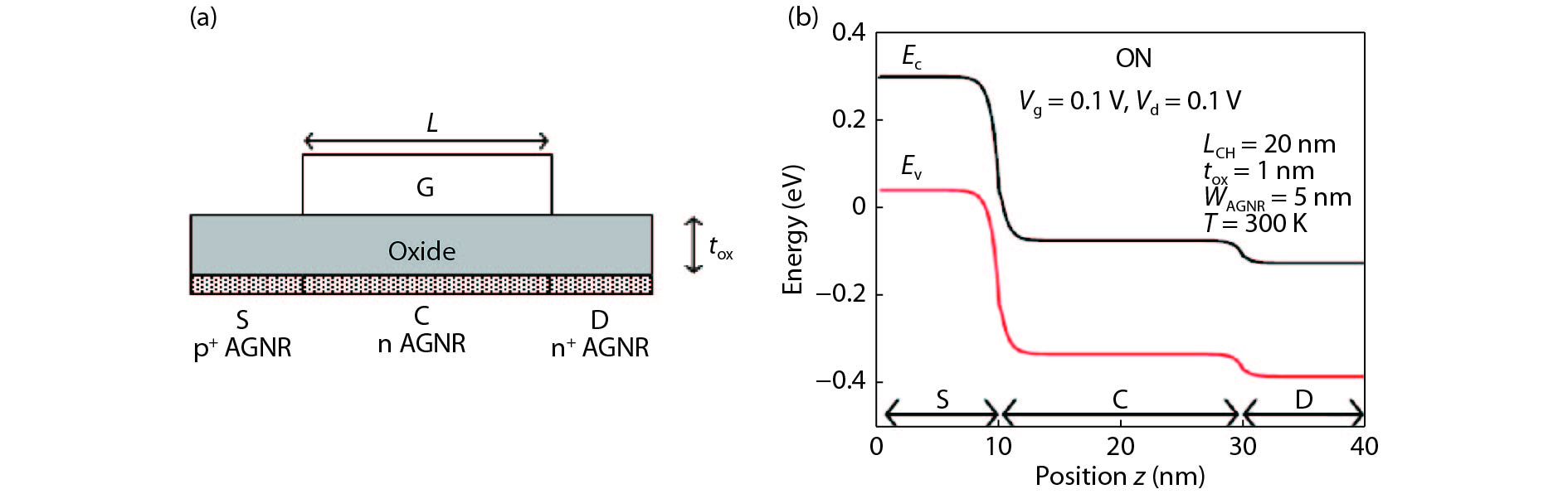
Fig. 1.
(Color online) (a) The device structure of the n-channel GNR-TFET. (b) The conduction band of the GNR-TFET after self-consistency achieved.
ARTICLES
Endi Suhendi1, , Lilik Hasanah1, Dadi Rusdiana1, Fatimah A. Noor2, Neny Kurniasih3 and Khairurrijal2
Corresponding author: Endi Suhendi, Email: endis@upi.edu
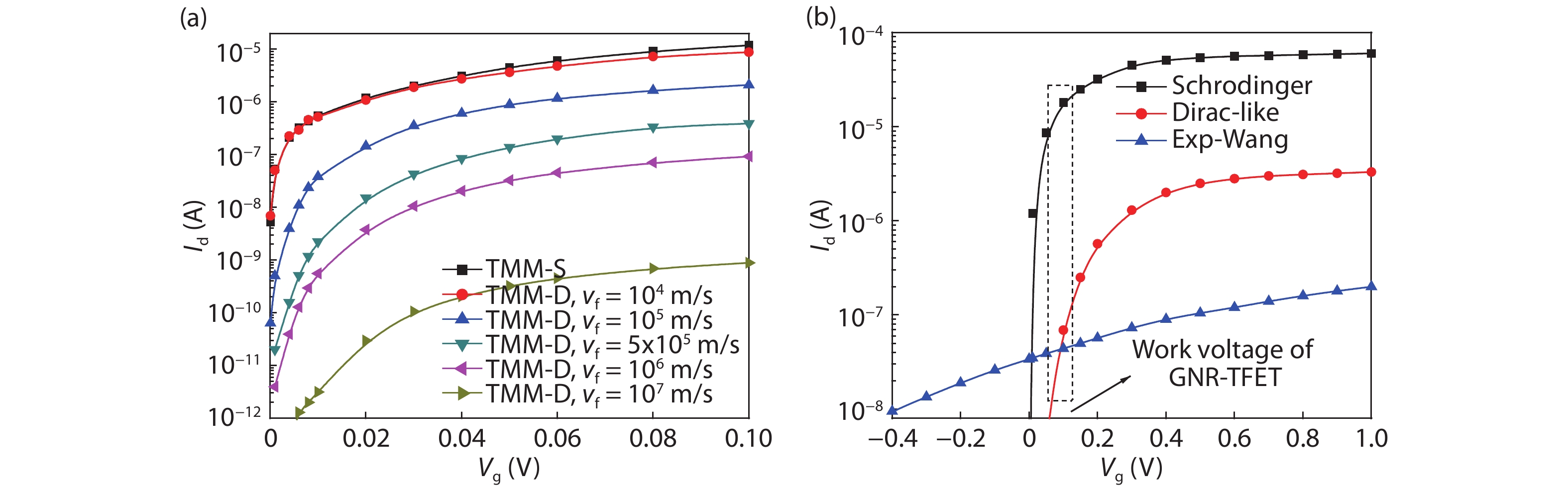
Abstract: The tunneling current in a graphene nanoribbon tunnel field effect transistor (GNR-TFET) has been quantum mechanically modeled. The tunneling current in the GNR-TFET was compared based on calculations of the Dirac-like equation and Schrödinger's equation. To calculate the electron transmittance, a numerical approach-namely the transfer matrix method (TMM)-was employed and the Launder formula was used to compute the tunneling current. The results suggest that the tunneling currents that were calculated using both equations have similar characteristics for the same parameters, even though they have different values. The tunneling currents that were calculated by applying the Dirac-like equation were lower than those calculated using Schrödinger's equation.
Keywords: graphene nanoribbon, tunnel field effect transistor, tunneling current, Schrödinger equation, Dirac-like equation
| [1] |
Novoselov K S, Geim A K, Morozov S V, et al. Electric field effect in atomically thin carbon films. Science, 2004, 306, 666 doi: 10.1126/science.1102896
|
| [2] |
Berger C, Song Z, Li X, et al. Electronic confinement and coherence in patterned epitaxial graphene. Science, 2006, 312, 1191 doi: 10.1126/science.1125925
|
| [3] |
Jena D, Fang T, Zhang Q, et al. Zener tunneling in semiconducting nanotube and graphene nanoribbon p−n junctions. Appl Phys Lett, 2008, 93, 112106 doi: 10.1063/1.2983744
|
| [4] |
Yansen W, Abdullah M, Khairurrijal. Application of airy function approach to model electron tunneling in graphene nanoribbon-based P−N junction diodes. Journal Nanosains & Nanoteknologi, 2010, 3, 18 doi: 2064728#.XNi_23duIbo
|
| [5] |
Brey L, Fertig H A. Electronic states of graphene nanoribbons. Phys Rev, 2006, B73, 235411 doi: 10.1103/PhysRevB.73.235411
|
| [6] |
Son Y W, Cohen M L, Loui S G. Energy gaps in graphene nanoribbons. Phys Rev Lett, 2006, 97, 216803 doi: 10.1103/PhysRevLett.97.216803
|
| [7] |
Huang B, Yan Q, Zhou G, et al. Making a field effect transistor on a single graphene nanoribbon by selective doping. Appl Phys Lett, 2007, 91, 253122 doi: 10.1063/1.2826547
|
| [8] |
Knoch J, Appenzeller J. Tunneling phenomena in carbon nanotube field-effect transistors. Phys. Status Solidi A, 2008, 205, 679 doi: 10.1002/pssa.v205:4
|
| [9] |
Katsnelson M I, Novoselov K S, Geim A K. Chiral tunneling and the Klein paradox in graphene. Nat Phys, 2006, 2, 620 doi: 10.1038/nphys384
|
| [10] |
Suhendi E, Syariati R, Noor F A, et al. Simulation of Dirac tunneling current of an armchair graphene nanoribbon-based p–n junction using a transfer matrix method. Adv Mater Res, 2014, 974, 205 doi: 10.4028/www.scientific.net/AMR.974
|
| [11] |
Hung Nguyen V, Bournel A, Dollfus P. Large peak-to-valley ratio of negative-differential-conductance in graphene p–n junctions. J Appl Phys, 2011, 109, 093706 doi: 10.1063/1.3587570
|
| [12] |
Nam Do P, Dollfus P. Negative differential resistance in zigzag-edge graphene nanoribbon junction. J Appl Phys, 2010, 107, 063705 doi: 10.1063/1.3340834
|
| [13] |
Xu X, Xu G, Cao J. Electron tunneling through a trapezoidal barrier in graphene. Jpn J Appl Phys, 2010, 49, 085201 doi: 10.1143/JJAP.49.085201
|
| [14] |
Suhendi E, Syariati R, Noor F A, et al. Modeling of Dirac electron tunneling current in bipolar transistor based on armchair graphene nanoribbon using a transfer matrix method. Adv Comput Sci Res, 2015, 5, 164 doi: 10.2991/iccst-15.2015.32
|
| [15] |
Chauhan J, Guo J. Assessment of high-frequency performance limits of graphene field-effect transistors. Nano Res, 2011, 4(6), 571 doi: 10.1007/s12274-011-0113-1
|
| [16] |
Mukherjee U, Banerjee S, Sarkar R, et al. Single quantum well p–n junction diode based on graphene nanoribbon. Graphene, 2015, 3(1), 6 doi: 10.1166/graph.2015.1057
|
| [17] |
Khatami Y, Kang J, Banerjee K. Graphene nanoribbon based negative resistance device for ultra-low voltage digital logic applications. App Phys Lett, 2013, 102, 043114 doi: 10.1063/1.4788684
|
| [18] |
Noei M, Moradinasab M, Fathipour M. A computational study of ballistic graphene nanoribbon field effect transistors. Phys E, 2012, 44, 1780 doi: 10.1016/j.physe.2011.12.018
|
| [19] |
Yang X, Chauhan J, Guo J, et al. Graphene tunneling FET and its applications in low-power circuit design. Proc of the 20th symposium on Great lakes symposium on VLSI, 2010, 263
|
| [20] |
Zhang Q, Fang T, Xing H, et al. Graphene nanoribbon tunnel transistors. Electron Device Lett, 2008, 29(12), 1344 doi: 10.1109/LED.2008.2005650
|
| [21] |
Abdolkader T M, Hassan M H, Fikry W. Solution of Schrödinger equation in double-gate MOSFETs using transfer matrix method. Electron Lett, 2004, 40(20), 20 doi: 10.1049/el:20045595
|
| [22] |
Noor F A, Abdullah M, Sukirno, et al. Comparison of electron transmittances and tunneling currents in an anisotropic TiN x/HfO2/SiO2/p-Si(100) metal–oxide–semiconductor (MOS) capacitor calculated using exponential- and airy-wavefunction approaches and a transfer matrix method. J Semicond, 2010, 31(12), 124002 doi: 10.1088/1674-4926/31/12/124002
|
| [23] |
Shangguan W Z, Zhou X, Chiah S B, et al. Compact gate-current model based on transfer-matrix method. J Appl Phys, 2005, 97, 123709 doi: 10.1063/1.1929885
|
| [24] |
Terrill K W, Hu C, Ko P K. An analytical model for the channel electric field in MOSFETs with graded-drain structures. IEEE Electron Device Lett, 1984, 5(11), 440 doi: 10.1109/EDL.1984.25980
|
| [25] |
Ferry D K, Goodnick S M, Bird J. Transport in nanostructures. Cambrige: Cambridge University Press, 2009
|
| [26] |
Tiwari M, Sharma K K, Rawat L S, et al. Impact of oxide thickness on gate capacitance, drain current and transconductance – a comprehensive analysis on MOSFET, nanowire FET and CNTFET devices. Int J Res Emerg Sci Technol, 2015, 2, 73 doi: 10.1109/TNANO.2013.2278021
|
| [27] |
Bolotin K I, Sikes K J, Jiang, Z, et al. Ultrahigh electron mobility in suspended graphene. Solid State Commun, 2008, 146, 351 doi: 10.1016/j.ssc.2008.02.024
|
| [28] |
Du X, Skachko I, Barker A, et al. Approaching ballistic transport in suspended graphene. Nature Nanotechnol, 2008, 3, 491 doi: 10.1038/nnano.2008.199
|
| [29] |
Sze S M. Semiconductor devices, physics and technology. New Jersey: John Wiley & Sons, 1985
|
| [30] |
Wang X, Ouyang Y, Li X, et al. Room-temperature all-semiconducting sub-10-nm graphene nanoribbon field-effect transistors. Phys Rev Lett, 2008, 100(20), 206803 doi: 10.1103/PhysRevLett.100.206803
|
| [31] |
Jimenez D. A current-voltage model for Schottky-barrier graphene based transistors. Nanotechnology, 2008, 19, 345204 doi: 10.1088/0957-4484/19/34/345204
|


Article views: 6083 Times PDF downloads: 84 Times Cited by: 0 Times
Received: 31 January 2019 Revised: 21 March 2019 Online: Accepted Manuscript: 30 April 2019Uncorrected proof: 13 May 2019Published: 05 June 2019
| Citation: |
Endi Suhendi, Lilik Hasanah, Dadi Rusdiana, Fatimah A. Noor, Neny Kurniasih, Khairurrijal. Comparison of tunneling currents in graphene nanoribbon tunnel field effect transistors calculated using Dirac-like equation and Schrödinger's equation[J]. Journal of Semiconductors, 2019, 40(6): 062002. doi: 10.1088/1674-4926/40/6/062002
****
E Suhendi, L Hasanah, D Rusdiana, F A Noor, N Kurniasih, Khairurrijal, Comparison of tunneling currents in graphene nanoribbon tunnel field effect transistors calculated using Dirac-like equation and Schrödinger\'s equation[J]. J. Semicond., 2019, 40(6): 062002. doi: 10.1088/1674-4926/40/6/062002.

|
| [1] |
Novoselov K S, Geim A K, Morozov S V, et al. Electric field effect in atomically thin carbon films. Science, 2004, 306, 666 doi: 10.1126/science.1102896
|
| [2] |
Berger C, Song Z, Li X, et al. Electronic confinement and coherence in patterned epitaxial graphene. Science, 2006, 312, 1191 doi: 10.1126/science.1125925
|
| [3] |
Jena D, Fang T, Zhang Q, et al. Zener tunneling in semiconducting nanotube and graphene nanoribbon p−n junctions. Appl Phys Lett, 2008, 93, 112106 doi: 10.1063/1.2983744
|
| [4] |
Yansen W, Abdullah M, Khairurrijal. Application of airy function approach to model electron tunneling in graphene nanoribbon-based P−N junction diodes. Journal Nanosains & Nanoteknologi, 2010, 3, 18 doi: 2064728#.XNi_23duIbo
|
| [5] |
Brey L, Fertig H A. Electronic states of graphene nanoribbons. Phys Rev, 2006, B73, 235411 doi: 10.1103/PhysRevB.73.235411
|
| [6] |
Son Y W, Cohen M L, Loui S G. Energy gaps in graphene nanoribbons. Phys Rev Lett, 2006, 97, 216803 doi: 10.1103/PhysRevLett.97.216803
|
| [7] |
Huang B, Yan Q, Zhou G, et al. Making a field effect transistor on a single graphene nanoribbon by selective doping. Appl Phys Lett, 2007, 91, 253122 doi: 10.1063/1.2826547
|
| [8] |
Knoch J, Appenzeller J. Tunneling phenomena in carbon nanotube field-effect transistors. Phys. Status Solidi A, 2008, 205, 679 doi: 10.1002/pssa.v205:4
|
| [9] |
Katsnelson M I, Novoselov K S, Geim A K. Chiral tunneling and the Klein paradox in graphene. Nat Phys, 2006, 2, 620 doi: 10.1038/nphys384
|
| [10] |
Suhendi E, Syariati R, Noor F A, et al. Simulation of Dirac tunneling current of an armchair graphene nanoribbon-based p–n junction using a transfer matrix method. Adv Mater Res, 2014, 974, 205 doi: 10.4028/www.scientific.net/AMR.974
|
| [11] |
Hung Nguyen V, Bournel A, Dollfus P. Large peak-to-valley ratio of negative-differential-conductance in graphene p–n junctions. J Appl Phys, 2011, 109, 093706 doi: 10.1063/1.3587570
|
| [12] |
Nam Do P, Dollfus P. Negative differential resistance in zigzag-edge graphene nanoribbon junction. J Appl Phys, 2010, 107, 063705 doi: 10.1063/1.3340834
|
| [13] |
Xu X, Xu G, Cao J. Electron tunneling through a trapezoidal barrier in graphene. Jpn J Appl Phys, 2010, 49, 085201 doi: 10.1143/JJAP.49.085201
|
| [14] |
Suhendi E, Syariati R, Noor F A, et al. Modeling of Dirac electron tunneling current in bipolar transistor based on armchair graphene nanoribbon using a transfer matrix method. Adv Comput Sci Res, 2015, 5, 164 doi: 10.2991/iccst-15.2015.32
|
| [15] |
Chauhan J, Guo J. Assessment of high-frequency performance limits of graphene field-effect transistors. Nano Res, 2011, 4(6), 571 doi: 10.1007/s12274-011-0113-1
|
| [16] |
Mukherjee U, Banerjee S, Sarkar R, et al. Single quantum well p–n junction diode based on graphene nanoribbon. Graphene, 2015, 3(1), 6 doi: 10.1166/graph.2015.1057
|
| [17] |
Khatami Y, Kang J, Banerjee K. Graphene nanoribbon based negative resistance device for ultra-low voltage digital logic applications. App Phys Lett, 2013, 102, 043114 doi: 10.1063/1.4788684
|
| [18] |
Noei M, Moradinasab M, Fathipour M. A computational study of ballistic graphene nanoribbon field effect transistors. Phys E, 2012, 44, 1780 doi: 10.1016/j.physe.2011.12.018
|
| [19] |
Yang X, Chauhan J, Guo J, et al. Graphene tunneling FET and its applications in low-power circuit design. Proc of the 20th symposium on Great lakes symposium on VLSI, 2010, 263
|
| [20] |
Zhang Q, Fang T, Xing H, et al. Graphene nanoribbon tunnel transistors. Electron Device Lett, 2008, 29(12), 1344 doi: 10.1109/LED.2008.2005650
|
| [21] |
Abdolkader T M, Hassan M H, Fikry W. Solution of Schrödinger equation in double-gate MOSFETs using transfer matrix method. Electron Lett, 2004, 40(20), 20 doi: 10.1049/el:20045595
|
| [22] |
Noor F A, Abdullah M, Sukirno, et al. Comparison of electron transmittances and tunneling currents in an anisotropic TiN x/HfO2/SiO2/p-Si(100) metal–oxide–semiconductor (MOS) capacitor calculated using exponential- and airy-wavefunction approaches and a transfer matrix method. J Semicond, 2010, 31(12), 124002 doi: 10.1088/1674-4926/31/12/124002
|
| [23] |
Shangguan W Z, Zhou X, Chiah S B, et al. Compact gate-current model based on transfer-matrix method. J Appl Phys, 2005, 97, 123709 doi: 10.1063/1.1929885
|
| [24] |
Terrill K W, Hu C, Ko P K. An analytical model for the channel electric field in MOSFETs with graded-drain structures. IEEE Electron Device Lett, 1984, 5(11), 440 doi: 10.1109/EDL.1984.25980
|
| [25] |
Ferry D K, Goodnick S M, Bird J. Transport in nanostructures. Cambrige: Cambridge University Press, 2009
|
| [26] |
Tiwari M, Sharma K K, Rawat L S, et al. Impact of oxide thickness on gate capacitance, drain current and transconductance – a comprehensive analysis on MOSFET, nanowire FET and CNTFET devices. Int J Res Emerg Sci Technol, 2015, 2, 73 doi: 10.1109/TNANO.2013.2278021
|
| [27] |
Bolotin K I, Sikes K J, Jiang, Z, et al. Ultrahigh electron mobility in suspended graphene. Solid State Commun, 2008, 146, 351 doi: 10.1016/j.ssc.2008.02.024
|
| [28] |
Du X, Skachko I, Barker A, et al. Approaching ballistic transport in suspended graphene. Nature Nanotechnol, 2008, 3, 491 doi: 10.1038/nnano.2008.199
|
| [29] |
Sze S M. Semiconductor devices, physics and technology. New Jersey: John Wiley & Sons, 1985
|
| [30] |
Wang X, Ouyang Y, Li X, et al. Room-temperature all-semiconducting sub-10-nm graphene nanoribbon field-effect transistors. Phys Rev Lett, 2008, 100(20), 206803 doi: 10.1103/PhysRevLett.100.206803
|
| [31] |
Jimenez D. A current-voltage model for Schottky-barrier graphene based transistors. Nanotechnology, 2008, 19, 345204 doi: 10.1088/0957-4484/19/34/345204
|

 WeChat ID
Journal of Semiconductors © 2017 All Rights Reserved 京ICP备05085259号-2

 DownLoad:

