J. Semicond. > 2019, Volume 40 > Issue 9 > 092001

ARTICLES

Broadband polarized photodetector based on p-BP/n-ReS2 heterojunction

Wenkai Zhu1, 2, Xia Wei1, 2, Faguang Yan1, 2, Quanshan Lv1, 2, Ce Hu1, 2 and Kaiyou Wang1, 2, 3, 4,

+ Author Affiliations

 Corresponding author: Kaiyou Wang, E-mail: kywang@semi.ac.cn

DOI: 10.1088/1674-4926/40/9/092001

PDF

Turn off MathJax

Abstract: Two-dimensional (2D) atomic crystals, such as graphene, black phosphorus (BP) and transition metal dichalcogenides (TMDCs) are attractive for use in optoelectronic devices, due to their unique crystal structures and optical absorption properties. In this study, we fabricated BP/ReS2 van der Waals (vdWs) heterojunction devices. The devices realized broadband photoresponse from visible to near infrared (NIR) (400–1800 nm) with stable and repeatable photoswitch characteristics, and the photoresponsivity reached 1.8 mA/W at 1550 nm. In addition, the polarization sensitive detection in the visible to NIR spectrum (532–1750 nm) was demonstrated, and the photodetector showed a highly polarization sensitive photocurrent with an anisotropy ratio as high as 6.44 at 1064 nm. Our study shows that van der Waals heterojunction is an effective way to realize the broadband polarization sensitive photodetection, which is of great significance to the realization and application of multi-functional devices based on 2D vdWs heterostructures.

Key words: broadbandpolarized photodetectionp-BP/n-ReS2vdWs herterojunction broadbandpolarized photodetectionvdWs heterojunction

Two dimensional (2D) van der Waals (vdWs) crystals, such as graphene[1], black phosphorus (BP)[2], silicene[3], group-IV monochalcogenides[4] and transition metal dichalcogenides (TMDCs)[5], are attractive for use in various field, such as electronics and optoelectronics[68], valleytronics[9], flexible devices[10], memory devices[11], sensors[12], due to their unique electronic, mechanical, thermal, optical properties. The vdWs crystals have atomically flat thickness and clean interfaces that are free of dangling bonds due to relatively weak van der Waals interactions among layers. This offers opportunities to stack different individual 2D materials into vdWs heterostructures without the limitations of lattice mismatch. The vdWs heterostructures have opened a new platform for fundamental research and device applications[13]. Broadband photodetector have great potential for optoelectronic applications, such as optical communication, imaging, night vision, environmental monitoring, and remote sensing[1418]. Polarization properties is another degree of freedom for light that is largely uncorrelated with spectral and intensity images, and thus has the ability to carry more information[16]. Therefore, the broadband polarization sensitive photodetector based on vdWs structure will promote the development of the next generation photodetectors.

Black phosphorus is a layered material, where each phosphorus atom is bonded covalently to three neighboring atoms forming a puckered orthorhombic lattice. The BP is a direct bandgap semiconductor. The band gap of BP is dependent on the number of layers, which increases from ~0.3 eV for bulk to ~2 eV for monolayer limit[19]. The ultrahigh carrier mobility of ~1000 cm2V−1s−1 was obtained in BP field effect transistor (FET) for a thickness of ~10 nm[2]. BP also has high in-plane anisotropy properties due to its different bond angles and lengths along the direction of armchair (AC) and zigzag (ZZ)[20, 21]. The hole mobility of BP can theoretically reach 10 000 to 26 000 cm2V−1s−1 for the monolayer (ZZ direction)[22]. Polarization sensitive broadband photodetectors based on BP FET have been demonstrated, which indicating BP is a promising candidate for broadband polarization sensitive photodetection[23].

Rhenium disulphide (ReS2) as a member of TMDCs also have been extensively investigated[24, 25]. ReS2 is a semiconductor with a single direct band gap of 1.55 eV that is nearly independent of the number of atomic layers[26, 27]. It exhibits a strong in-plane anisotropy in nature due to its stable Peierls distorted octahedral (1T) phase where the buckled S layers and zigzag Re chains along one of the lattice vectors in the plane[26, 28]. According to the reported ReS2 photodetectors, it shows an n-type behavior with the electron mobility of ~40 cm2V-1s-1, and a photoresponsivity of 103 A/W was achieved at low intensity of light, which implies ReS2 has a potential for sensitive photodetection[29, 30].

Recently, the reported BP-on-WSe2 heterostructure photodetector exhibits a broadband photoresponsivity in a spectral range of 400–1550 nm[19]. A similar photodetectors based on BP/ReS2 p–n diode were reported, which shows the photoresponse properties can be modified by adjusting the back gate voltage, however a high photoresponsivity achieved only in the ultraviolet (UV) band[31]. Another photodetector based on BP/ReS2 heterojunctions were stacked by controlling their crystal orientation, which exhibits a stronger polarization-dependent photocurrent characteristic in the visible region[32]. In this work, we systematically studied the variation of photoresponsivity and the polarization sensitive photocurrent anisotropy ratio of the BP/ReS2 heterojunction devices with the incident light power and wavelength. The devices realize broadband photoresponse from visible to near infrared (NIR) (400–1800 nm) with stable and repeatable photoswitch characteristics, and the photoresponsivities reaches 1.8 mA/W at 1550 nm. In addition, the polarization sensitive detection from the visible to NIR spectrum (532–1750 nm) was demonstrated, which shows a highly polarization sensitive photocurrent with an anisotropy ratio as high as 2.98 at 532 nm, 3.39 at 650 nm, 6.44 at 1064 nm, 5.5 at 1550 nm, and 4.3 at 1750 nm. Our study shows that the vdWs heterojunctions is an effective way to realize the broadband and polarized photodetection.

Fabrication of the BP/ReS2 heterojunction-based polarized photodetector devices. First, a BP (from HQ graphene) flake was exfoliated onto polydimethylsiloxane (PDMS) stamps by adhesive tape. The stamps are adhered to a glass slide. Under optical microscope, the BP flake with appropriate thickness and shape can be chosen. Afterwards, the target BP flake was transferred onto a 300 nm thick SiO2/Si substrate by using a site-controllable dry transfer method[33]. Then, using the same method, a ReS2 (from HQ graphene) flake was transferred onto the BP flake to fabricate a 2D heterojunction. Notably, the whole transfer processes were performed in a glove box to ensure a clean interface. Finally, the source and drain electrode regions were patterned by standard electron beam lithography, and Ta/Au (5/45 nm) layers were deposited on an ultrahigh vacuum evaporative sputtering system, followed by a lift-off process. The lift-off process was also performed in a glove box to avoid BP degradation. The thickness of both BP and ReS2 flakes were measured by atomic force microscopy (AFM) (Bruker Multimode 8). The device was stored in a small vacuum chamber with 2 × 10⁻⁵ mbar during the whole electric and optoelectric measurement processes.

Electrical and optoelectrical properties were measured using a semiconductor characterization system (Agilent Technology B1500A) and a lock-in amplifier (SR830) with a light chopper. The visible to NIR light illumination was provided by a Fianium WhiteLase supercontinuum laser source. The output light was tuned into monochromatic light by an Omni-λ300 monochromator. For the spatially-dependent photocurrent measurement, a microscope objective lens (50×), a lock-in amplifier (SR830) with a light chopper and a micromechanical stage were combined. Linearly polarized light was obtained by making a laser beam pass through a Glan-Taylor prism (polarizer) and a half-wave plate (HWP). The polarization direction of the light was controlled by rotating the HWP while keeping the incident laser power a constant.

Calculation details of the FET device mobility: The field-effect mobility can be calculated using the equation μ = (L/W)(d/ε0εrVds)(∆Ids/∆Vbg), where L and W are the length and width of the channel respectively, d is the oxide thickness, ε0 and εr are the permittivity of free space and the relative permittivity of the SiO2, and the last term is the slope of the transfer curve in the linear regime of the ON state.

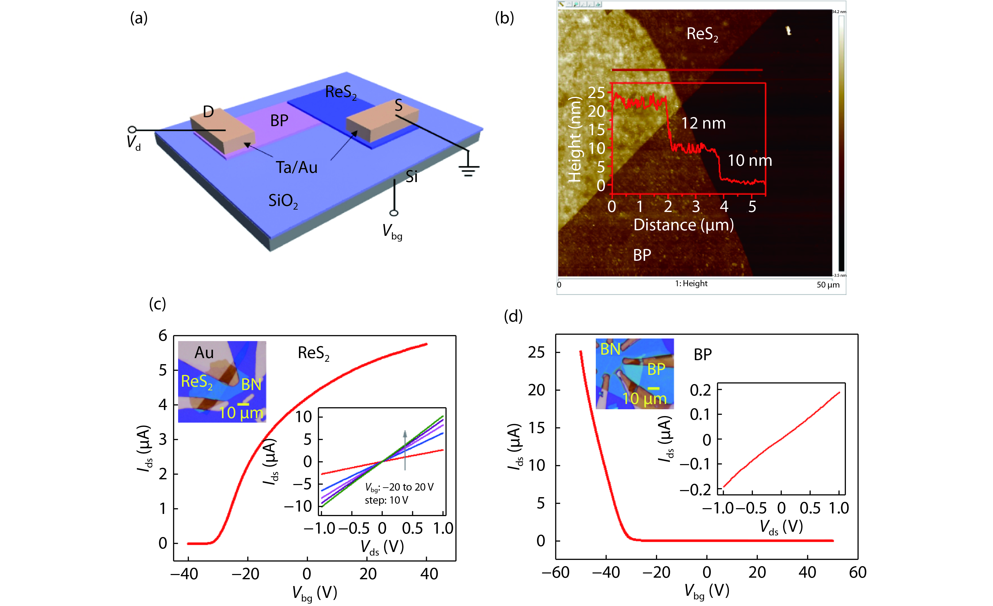
Characteristic of the BP/ReS2 heterojunction device. Fig. 1(a) presents a schematic of our heterojunction device. All of the devices were prepared by mechanical exfoliation and site-controllable dry transfer method. The detailed fabrication processes has been provided in the experimental section. An AFM image of the p-BP/n-ReS2 heterojunction is shown in Fig. 1(b), with the height profile along the red solid line being shown in the inset, indicating the thicknesses of BP (~10 nm) and ReS2 (~12 nm). We first performed the electrical characterizations of the ReS2 FET and BP FET at room temperature. Fig. 1(c) shows the transfer curve of the ReS2 FET with a linear plot of the source-drain current (Ids) versus back gate voltage (Vbg) at a fixed source–drain voltage (Vds = 0.5 V). The device shows an n-type FET behaviors with electron mobility of ~29 cm2V–1s–1 (see the experimental section for the calculation details), which is consistent with the reported value[30]. Optical microscope image of the ReS2 FET covered by ~10 nm thick BN is shown in the top inset of Fig. 1(c). The thickness of the ReS2 is about 6 nm. The Ids–Vds curves under different Vbg for the ReS2 FET have been presented in the bottom inset of Fig. 1(c). The linear IdsVds curves under low drain voltage indicates negligible Schottky barrier at the ReS2 and Au interfaces. Fig. 1(d) shows Ids as a function of Vbg for BP FET at room temperature and Vds = 0.5 V. This device showed a p-type FET behavior with hole mobility ~ 166 cm2V–1s–1. The top inset of Fig. 1(d) shows the optical microscope image of the BP FET covered by ~15 nm thick BN. The thickness of the BP is about 10 nm. The IdsVds curve of the BP FET is shown in the bottom inset of Fig. 1(d). The near-linear IdsVds curve shows a near ohmic contact between BP and Au.

Figure  1.  (Color online) (a) Structure schematic of BP/ReS2 heterojunction device. The source electrode (the contact connected to ReS2) is grounded. The drain electrode (the contact connected to BP) is applied a voltage Vd. (b) AFM image of p-BP/n-ReS2 heterojunction device. The inset shows the height profile along the red solid line, indicating the thicknesses of BP (~10 nm) and ReS2 (~12 nm). (c) The transfer curve of the ReS2 FET with Au contact was measured at room temperature and Vds = 0.5 V. Top inset: Optical microscope image of the ReS2 FET. The scale bar is 10 μm. The thickness of the ReS2 is about 6 nm. Bottom inset: Current–voltage (IdsVds) curves for different gate voltages (Vbg). (d) Ids as a function of Vbg for BP FET at room temperature and Vds = 0.5 V. Top inset: Optical microscope image of the BP FET. The thickness of the BP is about 10 nm. Bottom inset: IdsVds curve of the BP FET.

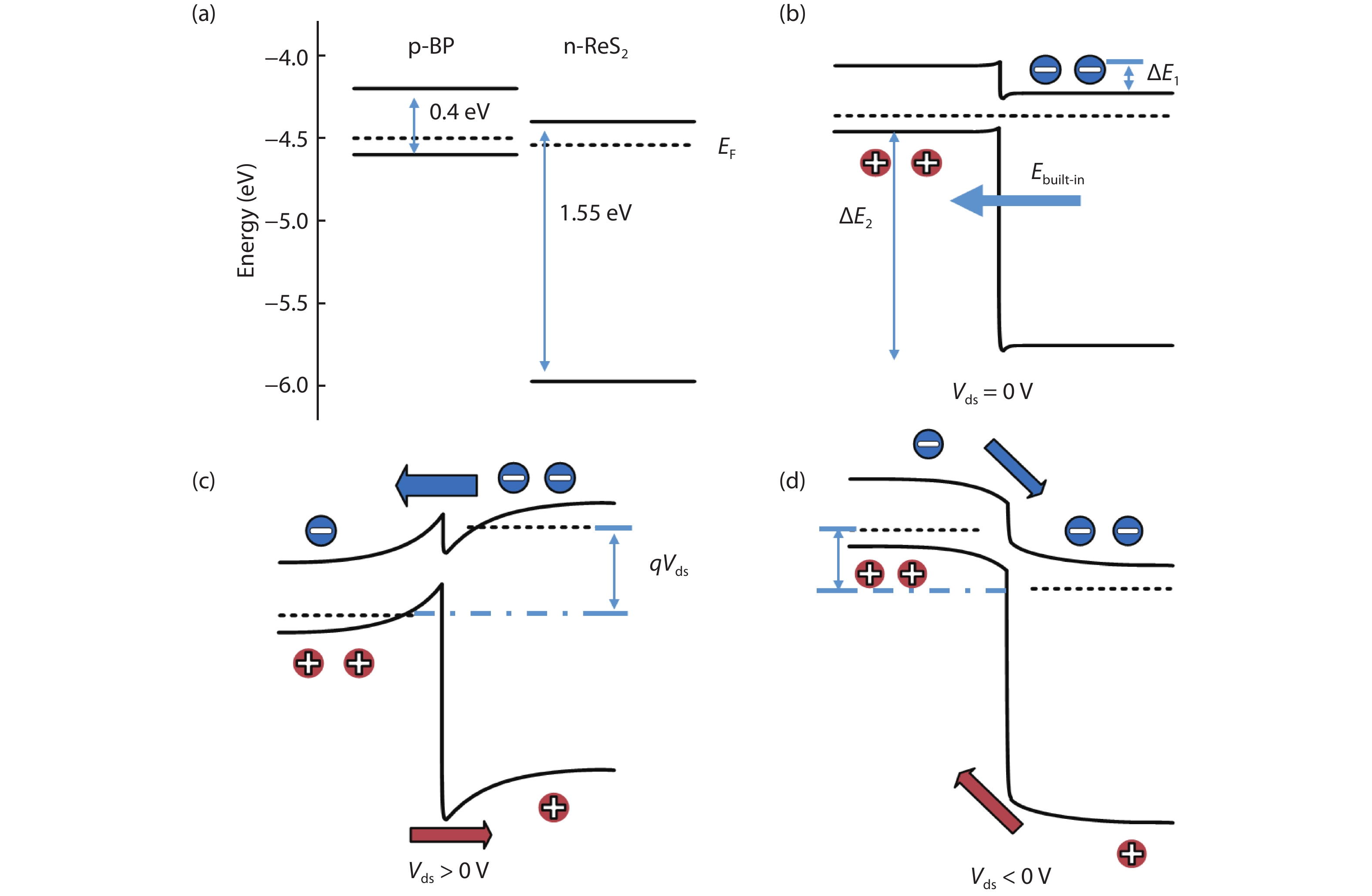
In addition to the conductive type of the materials, the energy band structure of the materials is also very important for construction of a p–n junction. The energy band diagrams of the heterojunction in the isolated and different bias states are illustrated in Figs. 2(a)2(d). Based on previous reports, the electron affinity and bandgap (Eg) of multilayer BP are around 4.2 and 0.4 eV, respectively[20, 22, 34]. For multilayer ReS2, the corresponding values are about 4.4 and 1.55 eV[26, 32]. Therefore, the BP/ReS2 heterojunction has a type-II band alignment because the conduction band minimum (EC) of BP lies above that of ReS2 by ∆EC = 0.2 eV, whereas the valence band maximum (EV) of ReS2 lies below (∆EV = 1.35 eV) that of BP. In addition, the valence band edge of BP lies below that of the conduction band edge of ReS2 by only 0.2 eV, which means the BP/ReS2 heterojunction can be easily electrostatic tuned to a broken-gap heterojunction with type-III band alignment, which can be used to explore the TFETs[35, 36]. Fig. 2(a) presents the band diagram for isolated few layers p-BP and n-ReS2. The built-in potential is formed when the two-layered materials are stacked together, which is indicated by blue arrow in Fig. 2(b). At Vds = 0 V, the minority carrier (electron) in BP crosses the small barrier and forms a small reverse current. As shown in Fig. 2(c), under positive bias, the electrons (majority carriers in ReS2) will transport to BP by overcoming the barrier height ∆E1. Meanwhile, the holes (majority carriers in BP) will travel to ReS2 by overcoming the barrier height ∆E2. Due to the larger ∆E2 compare to ∆E1, the current is dominated by the over-barrier free-electron transport (blue arrow). Fig. 2(d) shows the electrical field in the heterojunction is strongly enhanced under reverse bias. The minority carrier (electrons in BP and holes in ReS2) contributes to the conduction process.

Figure  2.  (Color online) (a) Band alignment for isolated p-BP and n-ReS2 layers. Electron affinities of BP and ReS2 are around 4.2 and 4.4 eV, respectively. (b–d) schematic band diagrams at the interface of the BP/ReS2 heterojunction at different applied voltages Vds ((b)zero bias, (c) positive bias and (d) negative bias). The transportation of electrons and holes are indicated by blue arrows and red arrows, respectively.

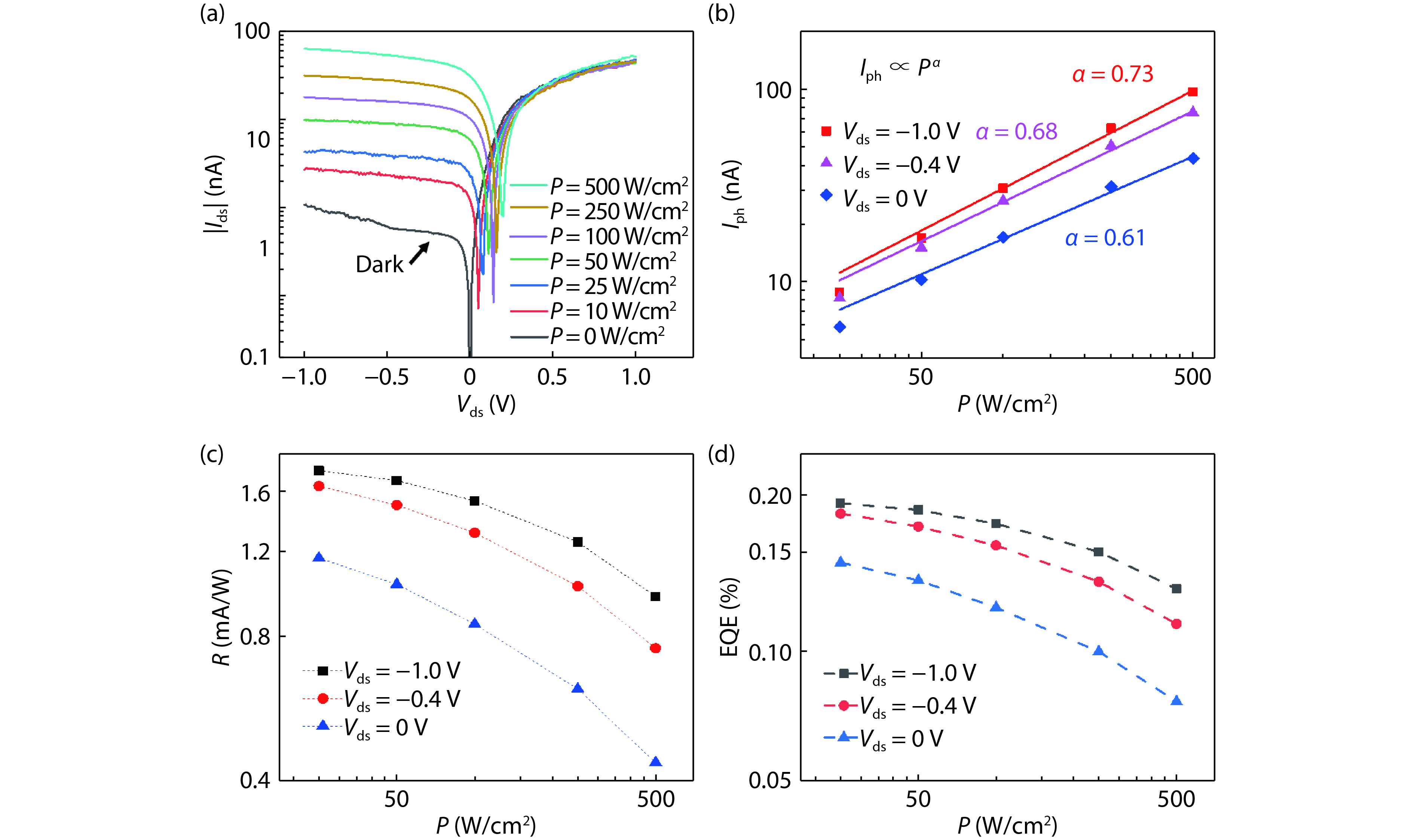
To investigate the responsivity of the device dependence on the illumination intensities, different illumination intensities P ranging from 0 to 500 W/cm2 are applied to the heterojunction device. Fig. 3(a) shows the |Ids|–Vds curves of the BP/ReS2 heterojunction device at room temperature in the dark and under illumination with a 1550 nm laser at various excitation intensities (P = 10, 25, 50, 100, 250, 500 W/cm2). The |Ids|–Vds curve of the device in the dark exhibits a clear rectifying behavior. The rectification ratio, defined as the ratio of the forward/reverse current, is about 50 at Vds = +1/–1 V. This behavior can be attributed to the formation of p–n diode within the atomically thin BP/ReS2 heterojunction (more details see band alignment of the BP/ReS2 heterojunction). The device exhibits a low dark current (~1.0 nA) at Vds = –1 V. Under a light illumination, electron-hole pairs are generated and separated by the electric field in the heterojunction, which generate the photocurrents. Photocurrent (Iph) is defined as the difference between drain currents with and without light-illumination (Iph = |IlightIdark|). Under reverse bias (Vds < 0 V), Iph increases with increasing the light intensity P. Iph can also be enhanced by increasing the reverse bias (shown in Fig. 3(b)). It can be explained by the increased electrical field in the heterojunction under reverse bias (Fig. 2(d)). The increased electrical field decreases the carrier transit time, thus reduces the recombination probability of the photo-generated electrons and holes. In addition, Iph exhibits a sublinear dependence on the incident light intensity P and follows a power law of IphPα, where α = 0.61, 0.68, and 0.73 at Vds = 0, –0.4 and –1 V, respectively. Larger value α can be obtained by applied a larger reverse bias, which also benefits from the shorter carrier transit time. The similar sublinear behavior has also been reported for other similar structures, such as ReS2 FETs[29], WSe2/graphene[37], MoS2/WS2 heterostrctures[38], and several of our previous works (WS2/GaSe, InSe/GaSe, WSe2/GaSe, MoTe2 photodetectors)[3942]. To quantify the photoresponse performance, the photoresponsivity (R = Iph/PS) of the heterojunction as a function of the illumination intensity at different applied voltages were extracted and shown in Fig. 3(c). The corresponding external quantum efficiency (EQE = hcR/eλ) of the device at different Vds (Vds = 0, –0.4, –1 V) were presented in Fig. 3(d). Here S is the in-plane area (~20 µm2) of the device, e is the electron charge, c is the speed of the light and h is Planck constant. All of two important factors increase with decreasing light intensity, consistent with the sublinear behavior of the photocurrent. Our device exhibits a photoresponsivity of R = 1.8 mA/W with corresponding EQE = 0.14% at Vds = –1 V under the wavelength 1550 nm. The photoresponsivity is comparable to most of similar vdWs heterojunction photodetectors reported recently, such as 4.36 mA/W in MoS2/WS2[43].

Figure  3.  (Color online) (a) |Ids|–Vds curves of the BP/ReS2 heterojunction device at room temperature in the dark and under illumination with a 1550 nm laser at various excitation intensities (P = 10, 25, 50, 100, 250, 500 W/cm2). (b) Photocurrent as a function of the illumination intensity at different Vds (Vds = 0, –0.4, –1 V). The solid lines are fits to the data. (c) Photoresponsivity (R) of the BP/ReS2 heterojunction device as a function of the illumination intensity at different Vds (Vds = 0, –0.4, –1 V). (d) The external quantum efficiency, EQE, of the heterojunction device as a function of the illumination intensity P at different Vds (Vds = 0, –0.4, –1 V). The wavelength of incident light is 1550 nm.

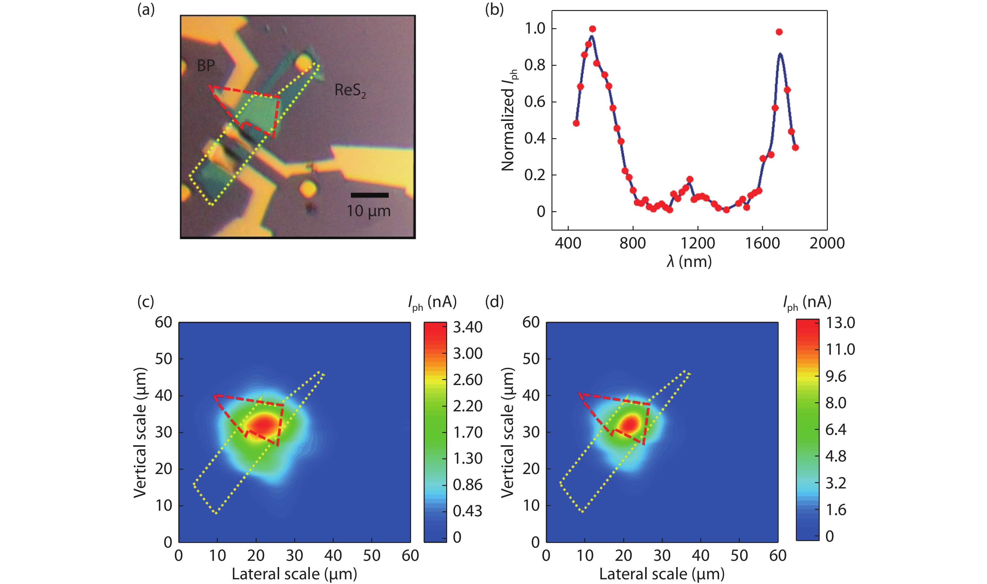
The image of the BP/ReS2 heterojunction device shown in Fig. 4(a), where the boundaries of each layer are indicated by dotted lines with different colors. The corresponding scale bar is 10 µm. Fig. 4(b) shows the normalized photocurrent as a function of the illumination wavelength at Vds = –1 V and illumination intensity P = 100 W/cm2, which demonstrates the BP/ReS2 heterojunction device exhibits obvious photoresponse over a broad spectral range (400–1800 nm), from the visible to near infrared. The maximum normalized Iph ~ 1 is obtained at wavelength of 550 nm, and the minimum normalized Iph ~ 0.013 is obtained at wavelength of 1025 nm. Therefore, the device can be used for broadband photodetection. ReS2 has the strongest absorption in the ultraviolet and visible band, but weaker absorption in the near infrared bands[44]. Meanwhile, BP has a natural narrow band gap, which has a strong absorption in visible and near infrared bands. As a result, a strong absorption at 550 nm of the device is induced by the light absorption properties of ReS2 and BP. Another strong absorption at 1710 nm of the device is dominated by the light absorption properties of BP. According to the reported results, the absorption peak position for a N-layer BP can be described using tight-binding model through the expression EN,n = 1.8 – 1.46cos(/(N + 1)), where the subband index n = 1…N[45]. The absorption peaks of 550 nm (2.25 eV) and 1720 nm (0.72 eV) in our device can be explained by n = 13, 5 when L = 20. In order to explore the origin of the photoresponse, scanning photocurrent maps were measured at both zero and negative biases. The corresponding photocurrent maps at zero and negative biases with 1550 nm laser excitation (illumination intensity P = 100 W/cm2) are shown in Figs. 4(c) and 4(d), respectively. The photocurrent map shows that the photoresponse of the overlapping region is strongly enhanced compared with the non-overlapping regions. It also demonstrates the formation of a p–n junction across the area of the BP/ReS2 interface where the photo-generated electrons and holes are separated and extracted more efficiently.

Figure  4.  (Color online) (a) Optical microscope image of the BP/ReS2 heterojunction device, component materials are outlined in different colors. (b) The normalized photocurrent as a function of the illumination wavelength at Vds = –1 V and illumination intensity P = 100 W/cm2. (c), (d) Scanning photocurrent microscope images of the BP/ReS2 heterojunction at Vds = 0 V (c) and –1 V (d) with illumination wavelength 1550 nm (illumination intensity P = 100 W/ cm2). The red dotted line outlines the BP flake and yellow dotted line outlines the ReS2 flake, respectively. The laser beam is focused by microscope objective lens (50×) and the diameter of the spot size is about 5 μm.

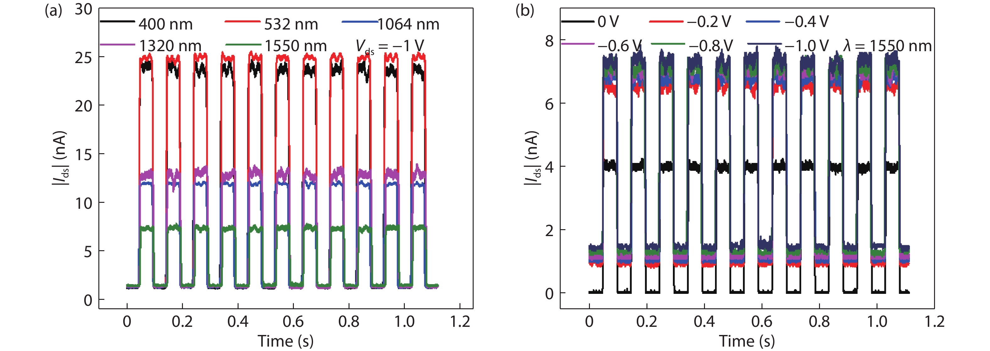
The excellent stability is an important condition for the application of photodetectors. For investigate the stability of the device, the device was illuminated by a laser with different wavelength (or under different Vds) and light intensity P = 50 W/cm2. Fig. 5(a) presents the time dependences of |Ids| during incident light switched on/off at Vds = –1 V with different wavelength (λ = 400, 532, 1064, 1320, 1550 nm), which shows the device can steady working over a broad spectral range, from visible to near infrared. In addition, the photoswitch ratio (Ilight/Idark) of the device is about 23 at 400 nm, 25 at 532 nm, 12 at 1064, 13 at 1320, and 7 at 1550 nm. Source–drain current |Ids| as a function of time with photoswitching at different Vds (Vds = 0, –0.2, –0.4, –0.6, –0.8, –1 V) shown in the Fig. 5(b). A stabilized photoresponsivity ~ 0.4 mA/W was achieved at λ = 1550 nm under zero bias, which shows the device can work as a self-driven near infrared photodetectors. Moreover, after many cycles, the photocurrent still responds in a similar fashion to the light, which exhibits excellent operation reversibility and stability.

Figure  5.  (Color online) (a) Time dependences of Ids during incident light switched on/off at Vds = –1 V with different wavelength (λ = 400, 532, 1064, 1320, 1550 nm). (b) Source–drain current Ids as a function of time with photoswitching at different Vds (Vds = 0, –0.2, –0.4, –0.6, –0.8, –1 V). The light intensity P = 50 W/cm2.

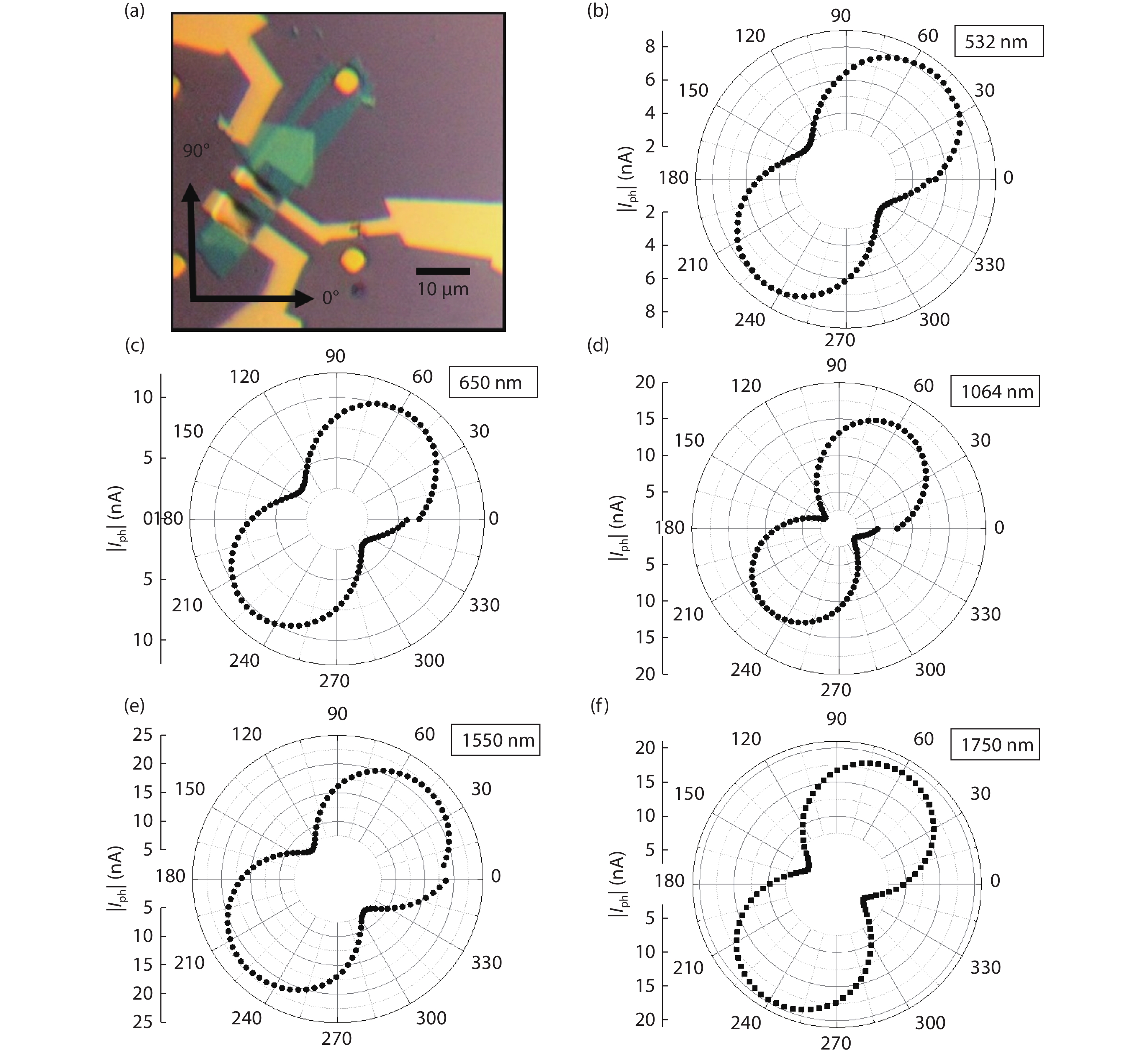
To examine the polarization sensitivity of the device, the device was illuminated by linearly polarized light with different polarized angle. The photocurrent as a function of polarized angle under different illumination wavelength is shown in Fig. 6. The optical microscope image of the BP/ReS2 heterojunction device is exhibited in Fig. 6(a). The angles of zero degree and 90 degree represents the rotation direction of the linearly polarized light. The anisotropic response in |Iph| plotted in the polar coordination at visible light wavelength of 532 nm (Fig. 6(b)) and 650 nm (Fig. 6(c)). The visible light intensity P = 25 W/cm2. Figs. 6(d)–6(f) presents the evolution of the |Iph| plotted in the polar coordination at near infrared light wavelength of 1064 nm (Fig. 6(d)), 1550 nm (Fig. 6(e)), and 1750 nm (Fig. 6(f)). The near infrared light intensity P = 100 W/cm2. The results show the device can act as a polarized photodetector over a broad spectral range (from 532 to 1750 nm). The double symmetry has been observed. The direction of the maximum photocurrent is perpendicular to the direction of the minimum photocurrent. The polarization sensitive absorption of the BP/ReS2 heterojunction photodetector is induced by crystal structure anisotropy. Because of the intrinsic low carrier mobility and high electron–hole recombination rate in ReS2[29], the polarization sensitivity of ReS2 is relatively low. Thus, the polarization sensitive absorption of the BP/ReS2 heterojunction device is mainly induced by crystal structure anisotropy of BP. The absorption of armchair-polarized light is always stronger than zigzag-polarized light for BP with all thicknesses, thus the two directions of the maximum photocurrent difference correspond to the orientation of BP crystal[45, 46]. It is worth noting the polarized photocurrent ratio Iph.max/Iph.min ≈ 2.98 at 532 nm, 3.39 at 650 nm, 6.44 at 1064 nm, 5.5 at 1550 nm, 4.3 at 1750 nm, which is larger than some other polarized sensitive anisotropy photodetectors, such as GeSe (1.09 at 532 nm)[47] and BP vertical p-n junction (3.5 at 1200 nm)[23]. The electrons transition process must meet the transition selection rule of momentum conservation, which can be expressed by the formulas: Eg = ћω and ћki ± ћqphonon = ћkf, where Eg is the bandgap of the semiconductor, ki and kf are the electron wave vectors at the valence band maximum (VBM) and conduction band minimum (CBM), respectively, ω is the angular frequency of the incident photon. In addition, the electric dipole transition probability P(ω) for photon absorption per unit time is introduced by Fermi Golden Rule: P(ω) = 2π/ћ|<φf|HeR|φi>|2δ(E(kf) – E(ki) – ћω), where ћ is the reduced Plank constant, HeR is the interaction of electromagnetic excitation. Here the transition occur from the initial states |φi> to the finial states |φf> with corresponding energy level E(ki) and E(kf). Moreover, the distribution and the overlap of VBM and CBM wave function is different along zigzag and armchair direction in BP, which will result in the difference of the |<φf|HeR|φi>|2 value[47] and wavelength dependent polarized photoresponse. In the near infrared region, BP has a large photoresponse to the polarized light along the armchair direction while the photoresponse of polarized light along the zigzag direction is small and changes little[23]. Thus the large polarized photocurrent ratios are observed in the near infrared region and the maximum polarized photocurrent ratio is 6.44 at 1064 nm.

Figure  6.  (Color online) (a) Optical microscope image of the BP/ReS2 heterojunction device. The angles of zero degree and 90 degree represents the rotation direction of the linearly polarized light. (b), (c) The anisotropic response in Iph plotted in the polar coordination at visible light wavelength of 532 and 650 nm. The visible light intensity P = 25 W cm2. (d–f) The evolution of the Iph plotted in the polar coordination at near infrared light wavelength of (d) 1064 nm, (e) 1550 nm, and (f) 1750 nm. The near infrared light intensity P = 100 W/ cm2. The Vds is fixed in –1 V.

In conclusion, we have fabricated BP/ReS2 vdWs heterojunction devices by dry-transfer of 2D flakes method. The devices realize broadband photoresponse from visible to near infrared (NIR) (400–1800 nm) with stable and repeatable photoswitch characteristics, and the photoresponsivities reached 1.8 mA/W at 1550 nm. In addition, the polarization sensitive detection form the visible to NIR spectrum (532–1750 nm) was demonstrated, which shows a highly polarization sensitive photocurrent with an anisotropy ratio as high as 2.98 at 532 nm, 3.39 at 650 nm, 6.44 at 1064 nm, 5.5 at 1550 nm, and 4.3 at 1750 nm. Because of the intrinsic low carrier mobility and high electron–hole recombination rate in ReS2, the polarization sensitivity of ReS2 is relatively low. Thus, the polarization sensitive absorption of the BP/ReS2 heterojunction device is mainly induced by crystal structure anisotropy of BP. Our study shows that van der Waals heterojunction is an effective way to realize the broadband polarization sensitive photodetection, which is of great significance to the application of multi-functional devices based on 2D vdWs heterostructures.

This work was supported by the National Key R&D Program of China (Grant No. 2017YFA0303400 and No.2017YFB0405700). This work was also supported by the NSFC Grant Nos. 61774144 and 11474272. The project was sponsored by Chinese Academy of Sciences, grant No. QYZDY-SSW-JSC020, XDPB12, and XDB28000000.


[1]
Novoselov K S, Geim A K, Morozov S V, et al. Electric field effect in atomically thin carbon films. Science, 2004, 306(5696), 666 doi: 10.1126/science.1102896
[2]
Li L, Yu Y, Ye G J, et al. Black phosphorus field-effect transistors. Nat Nanotechnol, 2014, 9, 372 doi: 10.1038/nnano.2014.35
[3]
Vogt P, De Padova P, Quaresima C, et al. Silicene: compelling experimental evidence for graphenelike two-dimensional silicon. Phys Rev Lett, 2012, 108(15), 155501 doi: 10.1103/PhysRevLett.108.155501
[4]
Gomes L C, Carvalho A. Phosphorene analogues: Isoelectronic two-dimensional group-IV monochalcogenides with orthorhombic structure. Phys Rev B, 2015, 92(8), 085406 doi: 10.1103/PhysRevB.92.085406
[5]
Splendiani A, Sun L, Zhang Y, et al. Emerging photoluminescence in monolayer MoS2. Nano Lett, 2010, 10(4), 1271 doi: 10.1021/nl903868w
[6]
Wang Q H, Kalantar-Zadeh K, Kis A, et al. Electronics and optoelectronics of two-dimensional transition metal dichalcogenides. Nat Nanotechnol, 2012, 7, 699 doi: 10.1038/nnano.2012.193
[7]
Cao Y, Cai K, Hu P, et al. Strong enhancement of photoresponsivity with shrinking the electrodes spacing in few layer GaSe photodetectors. Sci Rep, 2015, 5, 8130 doi: 10.1038/srep08130
[8]
Luo W, Cao Y, Hu P, et al. Gate tuning of high-performance InSe-based photodetectors using graphene electrodes. Adv Opt Mater, 2015, 3(10), 1418 doi: 10.1002/adom.201500190
[9]
Schaibley J R, Yu H, Clark G, et al. Valleytronics in 2D materials. Nat Rev Mater, 2016, 1, 16055 doi: 10.1038/natrevmats.2016.55
[10]
Akinwande D, Petrone N, Hone J. Two-dimensional flexible nanoelectronics. Nat Commun, 2014, 5, 5678 doi: 10.1038/ncomms6678
[11]
Feng Q, Yan F, Luo W, et al. Charge trap memory based on few-layer black phosphorus. Nanoscale, 2016, 8(5), 2686 doi: 10.1039/C5NR08065G
[12]
Rao C N R, Gopalakrishnan K, Maitra U. Comparative study of potential applications of graphene, MoS2, and other two-dimensional materials in energy devices, sensors, and related areas. ACS Appl Mater Interfaces, 2015, 7(15), 7809 doi: 10.1021/am509096x
[13]
Pizzocchero F, Gammelgaard L, Jessen B S, et al. The hot pick-up technique for batch assembly of van der Waals heterostructures. Nat Commun, 2016, 7, 11894 doi: 10.1038/ncomms11894
[14]
Konstantatos G, Sargent E H. Nanostructured materials for photon detection. Nat Nanotechnol, 2010, 5, 391 doi: 10.1038/nnano.2010.78
[15]
Gong C, Zhang Y, Chen W, et al. Electronic and optoelectronic applications based on 2D novel anisotropic transition metal dichalcogenides. Adv Sci, 2017, 4(12), 1700231 doi: 10.1002/advs.v4.12
[16]
Tyo J S, Goldstein D L, Chenault D B, et al. Review of passive imaging polarimetry for remote sensing applications. Appl Opt, 2006, 45(22), 5453 doi: 10.1364/AO.45.005453
[17]
Yan F, Wei Z, Wei X, et al. Toward high-performance photodetectors based on 2D materials: strategy on methods. Small Methods, 2018, 2(5), 1700349 doi: 10.1002/smtd.v2.5
[18]
Wei X, Yan F G, Shen C, et al. Photodetectors based on junctions of two-dimensional transition metal dichalcogenides. Chin Phys B, 2017, 26(3), 038504 doi: 10.1088/1674-1056/26/3/038504
[19]
Ye L, Wang P, Luo W, et al. Highly polarization sensitive infrared photodetector based on black phosphorus-on-WSe2 photogate vertical heterostructure. Nano Energy, 2017, 37, 53 doi: 10.1016/j.nanoen.2017.05.004
[20]
Tran V, Soklaski R, Liang Y, et al. Layer-controlled band gap and anisotropic excitons in few-layer black phosphorus. Phys Rev B, 2014, 89(23), 235319 doi: 10.1103/PhysRevB.89.235319
[21]
Zhou Z, Cui Y, Tan P H, et al. Optical and electrical properties of two-dimensional anisotropic materials. J Semicond, 2019, 40(6), 061001 doi: 10.1088/1674-4926/40/6/061001
[22]
Qiao J, Kong X, Hu Z X, et al. High-mobility transport anisotropy and linear dichroism in few-layer black phosphorus. Nat Commun, 2014, 5, 4475 doi: 10.1038/ncomms5475
[23]
Yuan H, Liu X, Afshinmanesh F, et al. Polarization-sensitive broadband photodetector using a black phosphorus vertical p–n junction. Nat Nanotechnol, 2015, 10, 707 doi: 10.1038/nnano.2015.112
[24]
Zhang E, Jin Y, Yuan X, et al. ReS2-based field-effect transistors and photodetectors. Adv Funct Mater, 2015, 25(26), 4076 doi: 10.1002/adfm.v25.26
[25]
Rahman M, Davey K, Qiao S Z. Advent of 2D rhenium disulfide (ReS2): fundamentals to applications. Adv Funct Mater, 2017, 27(10), 1606129 doi: 10.1002/adfm.v27.10
[26]
Tongay S, Sahin H, Ko C, et al. Monolayer behaviour in bulk ReS2 due to electronic and vibrational decoupling. Nat Commun, 2014, 5, 3252 doi: 10.1038/ncomms4252
[27]
Pradhan N R, McCreary A, Rhodes D, et al. Metal to insulator quantum-phase transition in few-layered ReS2. Nano Lett, 2015, 15(12), 8377 doi: 10.1021/acs.nanolett.5b04100
[28]
Lin Y C, Komsa H P, Yeh C H, et al. Single-layer ReS2: two-dimensional semiconductor with tunable in-plane anisotropy. ACS Nano, 2015, 9(11), 11249 doi: 10.1021/acsnano.5b04851
[29]
Liu F, Zheng S, He X, et al. Highly sensitive detection of polarized light using anisotropic 2D ReS2. Adv Funct Mater, 2016, 26(8), 1169 doi: 10.1002/adfm.v26.8
[30]
Liu E, Long M, Zeng J, et al. High responsivity phototransistors based on few-layer ReS2 for weak signal detection. Adv Funct Mater, 2016, 26(12), 1938 doi: 10.1002/adfm.201504408
[31]
Cao S, Xing Y, Han J, et al. Ultrahigh-photoresponsive UV photodetector based on a BP/ReS2 heterostructure p–n diode. Nanoscale, 2018, 10(35), 16805 doi: 10.1039/C8NR05291C
[32]
Li X K, Gao X G, Su B W, et al. Polarization-dependent photocurrent of black phosphorus/rhenium disulfide heterojunctions. Adv Mater Interfaces, 2018, 5(22), 1800960 doi: 10.1002/admi.v5.22
[33]
Castellanos-Gomez A, Buscema M, Molenaar R, et al. Deterministic transfer of two-dimensional materials by all-dry viscoelastic stamping. 2D Mater, 2014, 1(1), 011002 doi: 10.1088/2053-1583/1/1/011002
[34]
Perello D J, Chae S H, Song S, et al. High-performance n-type black phosphorus transistors with type control via thickness and contact-metal engineering. Nat Commun, 2015, 6, 7809 doi: 10.1038/ncomms8809
[35]
Shim J, Oh S, Kang D H, et al. Phosphorene/rhenium disulfide heterojunction-based negative differential resistance device for multi-valued logic. Nat Commun, 2016, 7, 13413 doi: 10.1038/ncomms13413
[36]
Jo S H, Lee H W, Shim J, et al. Highly efficient infrared photodetection in a gate-controllable Van der Waals heterojunction with staggered bandgap alignment. Adv Sci, 2018, 5(4), 1700423 doi: 10.1002/advs.v5.4
[37]
Massicotte M, Schmidt P, Vialla F, et al. Picosecond photoresponse in van der Waals heterostructures. Nat Nanotechnol, 2015, 11, 42 doi: 10.1038/nnano.2015.227
[38]
Xue Y, Zhang Y, Liu Y, et al. Scalable production of a few-layer MoS2/WS2 vertical heterojunction array and its application for photodetectors. ACS Nano, 2016, 10(1), 573 doi: 10.1021/acsnano.5b05596
[39]
Lv Q, Yan F, Wei X, et al. High-performance, self-driven photodetector based on graphene sandwiched GaSe/WS2 heterojunction. Adv Opt Mater, 2018, 6(2), 1700490 doi: 10.1002/adom.v6.2
[40]
Yan F, Zhao L, Patane A, et al. Fast, multicolor photodetection with graphene-contacted p-GaSe/n-InSe van der Waals heterostructures. Nanotechnology, 2017, 28(27), 27L doi: 10.1088/1361-6528/aa749e
[41]
Wei X, Yan F, Lv Q, et al. Fast gate-tunable photodetection in the graphene sandwiched WSe2/GaSe heterojunctions. Nanoscale, 2017, 9(24), 8388 doi: 10.1039/C7NR03124F
[42]
Wei X, Yan F, Lv Q, et al. Enhanced photoresponse in MoTe2 photodetectors with asymmetric graphene contacts. Adv Opt Mater, 2019, 0(0), 1900190
[43]
Wu W, Zhang Q, Zhou X, et al. Self-powered photovoltaic photodetector established on lateral monolayer MoS2-WS2 heterostructures. Nano Energy, 2018, 51, 45 doi: 10.1016/j.nanoen.2018.06.049
[44]
Liu H, Xu B, Liu J M, et al. Highly efficient and ultrastable visible-light photocatalytic water splitting over ReS2. Phys Chem Chem Phys, 2016, 18(21), 14222 doi: 10.1039/C6CP01007E
[45]
Huang S, Ling X. Black phosphorus: optical characterization, properties and applications. Small, 2017, 13(38), 1700823 doi: 10.1002/smll.201700823
[46]
Ling X, Huang S, Hasdeo E H, et al. Anisotropic electron-photon and electron-phonon interactions in black phosphorus. Nano Lett, 2016, 16(4), 2260 doi: 10.1021/acs.nanolett.5b04540
[47]
Wang X, Li Y, Huang L, et al. Short-wave near-infrared linear dichroism of two-dimensional germanium selenide. J Am Chem Soc, 2017, 139(42), 14976 doi: 10.1021/jacs.7b06314
Fig. 1.  (Color online) (a) Structure schematic of BP/ReS2 heterojunction device. The source electrode (the contact connected to ReS2) is grounded. The drain electrode (the contact connected to BP) is applied a voltage Vd. (b) AFM image of p-BP/n-ReS2 heterojunction device. The inset shows the height profile along the red solid line, indicating the thicknesses of BP (~10 nm) and ReS2 (~12 nm). (c) The transfer curve of the ReS2 FET with Au contact was measured at room temperature and Vds = 0.5 V. Top inset: Optical microscope image of the ReS2 FET. The scale bar is 10 μm. The thickness of the ReS2 is about 6 nm. Bottom inset: Current–voltage (IdsVds) curves for different gate voltages (Vbg). (d) Ids as a function of Vbg for BP FET at room temperature and Vds = 0.5 V. Top inset: Optical microscope image of the BP FET. The thickness of the BP is about 10 nm. Bottom inset: IdsVds curve of the BP FET.

Fig. 2.  (Color online) (a) Band alignment for isolated p-BP and n-ReS2 layers. Electron affinities of BP and ReS2 are around 4.2 and 4.4 eV, respectively. (b–d) schematic band diagrams at the interface of the BP/ReS2 heterojunction at different applied voltages Vds ((b)zero bias, (c) positive bias and (d) negative bias). The transportation of electrons and holes are indicated by blue arrows and red arrows, respectively.

Fig. 3.  (Color online) (a) |Ids|–Vds curves of the BP/ReS2 heterojunction device at room temperature in the dark and under illumination with a 1550 nm laser at various excitation intensities (P = 10, 25, 50, 100, 250, 500 W/cm2). (b) Photocurrent as a function of the illumination intensity at different Vds (Vds = 0, –0.4, –1 V). The solid lines are fits to the data. (c) Photoresponsivity (R) of the BP/ReS2 heterojunction device as a function of the illumination intensity at different Vds (Vds = 0, –0.4, –1 V). (d) The external quantum efficiency, EQE, of the heterojunction device as a function of the illumination intensity P at different Vds (Vds = 0, –0.4, –1 V). The wavelength of incident light is 1550 nm.

Fig. 4.  (Color online) (a) Optical microscope image of the BP/ReS2 heterojunction device, component materials are outlined in different colors. (b) The normalized photocurrent as a function of the illumination wavelength at Vds = –1 V and illumination intensity P = 100 W/cm2. (c), (d) Scanning photocurrent microscope images of the BP/ReS2 heterojunction at Vds = 0 V (c) and –1 V (d) with illumination wavelength 1550 nm (illumination intensity P = 100 W/ cm2). The red dotted line outlines the BP flake and yellow dotted line outlines the ReS2 flake, respectively. The laser beam is focused by microscope objective lens (50×) and the diameter of the spot size is about 5 μm.

Fig. 5.  (Color online) (a) Time dependences of Ids during incident light switched on/off at Vds = –1 V with different wavelength (λ = 400, 532, 1064, 1320, 1550 nm). (b) Source–drain current Ids as a function of time with photoswitching at different Vds (Vds = 0, –0.2, –0.4, –0.6, –0.8, –1 V). The light intensity P = 50 W/cm2.

Fig. 6.  (Color online) (a) Optical microscope image of the BP/ReS2 heterojunction device. The angles of zero degree and 90 degree represents the rotation direction of the linearly polarized light. (b), (c) The anisotropic response in Iph plotted in the polar coordination at visible light wavelength of 532 and 650 nm. The visible light intensity P = 25 W cm2. (d–f) The evolution of the Iph plotted in the polar coordination at near infrared light wavelength of (d) 1064 nm, (e) 1550 nm, and (f) 1750 nm. The near infrared light intensity P = 100 W/ cm2. The Vds is fixed in –1 V.

[1]
Novoselov K S, Geim A K, Morozov S V, et al. Electric field effect in atomically thin carbon films. Science, 2004, 306(5696), 666 doi: 10.1126/science.1102896
[2]
Li L, Yu Y, Ye G J, et al. Black phosphorus field-effect transistors. Nat Nanotechnol, 2014, 9, 372 doi: 10.1038/nnano.2014.35
[3]
Vogt P, De Padova P, Quaresima C, et al. Silicene: compelling experimental evidence for graphenelike two-dimensional silicon. Phys Rev Lett, 2012, 108(15), 155501 doi: 10.1103/PhysRevLett.108.155501
[4]
Gomes L C, Carvalho A. Phosphorene analogues: Isoelectronic two-dimensional group-IV monochalcogenides with orthorhombic structure. Phys Rev B, 2015, 92(8), 085406 doi: 10.1103/PhysRevB.92.085406
[5]
Splendiani A, Sun L, Zhang Y, et al. Emerging photoluminescence in monolayer MoS2. Nano Lett, 2010, 10(4), 1271 doi: 10.1021/nl903868w
[6]
Wang Q H, Kalantar-Zadeh K, Kis A, et al. Electronics and optoelectronics of two-dimensional transition metal dichalcogenides. Nat Nanotechnol, 2012, 7, 699 doi: 10.1038/nnano.2012.193
[7]
Cao Y, Cai K, Hu P, et al. Strong enhancement of photoresponsivity with shrinking the electrodes spacing in few layer GaSe photodetectors. Sci Rep, 2015, 5, 8130 doi: 10.1038/srep08130
[8]
Luo W, Cao Y, Hu P, et al. Gate tuning of high-performance InSe-based photodetectors using graphene electrodes. Adv Opt Mater, 2015, 3(10), 1418 doi: 10.1002/adom.201500190
[9]
Schaibley J R, Yu H, Clark G, et al. Valleytronics in 2D materials. Nat Rev Mater, 2016, 1, 16055 doi: 10.1038/natrevmats.2016.55
[10]
Akinwande D, Petrone N, Hone J. Two-dimensional flexible nanoelectronics. Nat Commun, 2014, 5, 5678 doi: 10.1038/ncomms6678
[11]
Feng Q, Yan F, Luo W, et al. Charge trap memory based on few-layer black phosphorus. Nanoscale, 2016, 8(5), 2686 doi: 10.1039/C5NR08065G
[12]
Rao C N R, Gopalakrishnan K, Maitra U. Comparative study of potential applications of graphene, MoS2, and other two-dimensional materials in energy devices, sensors, and related areas. ACS Appl Mater Interfaces, 2015, 7(15), 7809 doi: 10.1021/am509096x
[13]
Pizzocchero F, Gammelgaard L, Jessen B S, et al. The hot pick-up technique for batch assembly of van der Waals heterostructures. Nat Commun, 2016, 7, 11894 doi: 10.1038/ncomms11894
[14]
Konstantatos G, Sargent E H. Nanostructured materials for photon detection. Nat Nanotechnol, 2010, 5, 391 doi: 10.1038/nnano.2010.78
[15]
Gong C, Zhang Y, Chen W, et al. Electronic and optoelectronic applications based on 2D novel anisotropic transition metal dichalcogenides. Adv Sci, 2017, 4(12), 1700231 doi: 10.1002/advs.v4.12
[16]
Tyo J S, Goldstein D L, Chenault D B, et al. Review of passive imaging polarimetry for remote sensing applications. Appl Opt, 2006, 45(22), 5453 doi: 10.1364/AO.45.005453
[17]
Yan F, Wei Z, Wei X, et al. Toward high-performance photodetectors based on 2D materials: strategy on methods. Small Methods, 2018, 2(5), 1700349 doi: 10.1002/smtd.v2.5
[18]
Wei X, Yan F G, Shen C, et al. Photodetectors based on junctions of two-dimensional transition metal dichalcogenides. Chin Phys B, 2017, 26(3), 038504 doi: 10.1088/1674-1056/26/3/038504
[19]
Ye L, Wang P, Luo W, et al. Highly polarization sensitive infrared photodetector based on black phosphorus-on-WSe2 photogate vertical heterostructure. Nano Energy, 2017, 37, 53 doi: 10.1016/j.nanoen.2017.05.004
[20]
Tran V, Soklaski R, Liang Y, et al. Layer-controlled band gap and anisotropic excitons in few-layer black phosphorus. Phys Rev B, 2014, 89(23), 235319 doi: 10.1103/PhysRevB.89.235319
[21]
Zhou Z, Cui Y, Tan P H, et al. Optical and electrical properties of two-dimensional anisotropic materials. J Semicond, 2019, 40(6), 061001 doi: 10.1088/1674-4926/40/6/061001
[22]
Qiao J, Kong X, Hu Z X, et al. High-mobility transport anisotropy and linear dichroism in few-layer black phosphorus. Nat Commun, 2014, 5, 4475 doi: 10.1038/ncomms5475
[23]
Yuan H, Liu X, Afshinmanesh F, et al. Polarization-sensitive broadband photodetector using a black phosphorus vertical p–n junction. Nat Nanotechnol, 2015, 10, 707 doi: 10.1038/nnano.2015.112
[24]
Zhang E, Jin Y, Yuan X, et al. ReS2-based field-effect transistors and photodetectors. Adv Funct Mater, 2015, 25(26), 4076 doi: 10.1002/adfm.v25.26
[25]
Rahman M, Davey K, Qiao S Z. Advent of 2D rhenium disulfide (ReS2): fundamentals to applications. Adv Funct Mater, 2017, 27(10), 1606129 doi: 10.1002/adfm.v27.10
[26]
Tongay S, Sahin H, Ko C, et al. Monolayer behaviour in bulk ReS2 due to electronic and vibrational decoupling. Nat Commun, 2014, 5, 3252 doi: 10.1038/ncomms4252
[27]
Pradhan N R, McCreary A, Rhodes D, et al. Metal to insulator quantum-phase transition in few-layered ReS2. Nano Lett, 2015, 15(12), 8377 doi: 10.1021/acs.nanolett.5b04100
[28]
Lin Y C, Komsa H P, Yeh C H, et al. Single-layer ReS2: two-dimensional semiconductor with tunable in-plane anisotropy. ACS Nano, 2015, 9(11), 11249 doi: 10.1021/acsnano.5b04851
[29]
Liu F, Zheng S, He X, et al. Highly sensitive detection of polarized light using anisotropic 2D ReS2. Adv Funct Mater, 2016, 26(8), 1169 doi: 10.1002/adfm.v26.8
[30]
Liu E, Long M, Zeng J, et al. High responsivity phototransistors based on few-layer ReS2 for weak signal detection. Adv Funct Mater, 2016, 26(12), 1938 doi: 10.1002/adfm.201504408
[31]
Cao S, Xing Y, Han J, et al. Ultrahigh-photoresponsive UV photodetector based on a BP/ReS2 heterostructure p–n diode. Nanoscale, 2018, 10(35), 16805 doi: 10.1039/C8NR05291C
[32]
Li X K, Gao X G, Su B W, et al. Polarization-dependent photocurrent of black phosphorus/rhenium disulfide heterojunctions. Adv Mater Interfaces, 2018, 5(22), 1800960 doi: 10.1002/admi.v5.22
[33]
Castellanos-Gomez A, Buscema M, Molenaar R, et al. Deterministic transfer of two-dimensional materials by all-dry viscoelastic stamping. 2D Mater, 2014, 1(1), 011002 doi: 10.1088/2053-1583/1/1/011002
[34]
Perello D J, Chae S H, Song S, et al. High-performance n-type black phosphorus transistors with type control via thickness and contact-metal engineering. Nat Commun, 2015, 6, 7809 doi: 10.1038/ncomms8809
[35]
Shim J, Oh S, Kang D H, et al. Phosphorene/rhenium disulfide heterojunction-based negative differential resistance device for multi-valued logic. Nat Commun, 2016, 7, 13413 doi: 10.1038/ncomms13413
[36]
Jo S H, Lee H W, Shim J, et al. Highly efficient infrared photodetection in a gate-controllable Van der Waals heterojunction with staggered bandgap alignment. Adv Sci, 2018, 5(4), 1700423 doi: 10.1002/advs.v5.4
[37]
Massicotte M, Schmidt P, Vialla F, et al. Picosecond photoresponse in van der Waals heterostructures. Nat Nanotechnol, 2015, 11, 42 doi: 10.1038/nnano.2015.227
[38]
Xue Y, Zhang Y, Liu Y, et al. Scalable production of a few-layer MoS2/WS2 vertical heterojunction array and its application for photodetectors. ACS Nano, 2016, 10(1), 573 doi: 10.1021/acsnano.5b05596
[39]
Lv Q, Yan F, Wei X, et al. High-performance, self-driven photodetector based on graphene sandwiched GaSe/WS2 heterojunction. Adv Opt Mater, 2018, 6(2), 1700490 doi: 10.1002/adom.v6.2
[40]
Yan F, Zhao L, Patane A, et al. Fast, multicolor photodetection with graphene-contacted p-GaSe/n-InSe van der Waals heterostructures. Nanotechnology, 2017, 28(27), 27L doi: 10.1088/1361-6528/aa749e
[41]
Wei X, Yan F, Lv Q, et al. Fast gate-tunable photodetection in the graphene sandwiched WSe2/GaSe heterojunctions. Nanoscale, 2017, 9(24), 8388 doi: 10.1039/C7NR03124F
[42]
Wei X, Yan F, Lv Q, et al. Enhanced photoresponse in MoTe2 photodetectors with asymmetric graphene contacts. Adv Opt Mater, 2019, 0(0), 1900190
[43]
Wu W, Zhang Q, Zhou X, et al. Self-powered photovoltaic photodetector established on lateral monolayer MoS2-WS2 heterostructures. Nano Energy, 2018, 51, 45 doi: 10.1016/j.nanoen.2018.06.049
[44]
Liu H, Xu B, Liu J M, et al. Highly efficient and ultrastable visible-light photocatalytic water splitting over ReS2. Phys Chem Chem Phys, 2016, 18(21), 14222 doi: 10.1039/C6CP01007E
[45]
Huang S, Ling X. Black phosphorus: optical characterization, properties and applications. Small, 2017, 13(38), 1700823 doi: 10.1002/smll.201700823
[46]
Ling X, Huang S, Hasdeo E H, et al. Anisotropic electron-photon and electron-phonon interactions in black phosphorus. Nano Lett, 2016, 16(4), 2260 doi: 10.1021/acs.nanolett.5b04540
[47]
Wang X, Li Y, Huang L, et al. Short-wave near-infrared linear dichroism of two-dimensional germanium selenide. J Am Chem Soc, 2017, 139(42), 14976 doi: 10.1021/jacs.7b06314
1

Broadband full-stokes polarimeter based on ReS2 nanobelts

Tinghao Lin, Wendian Yao, Zeyi Liu, Haizhen Wang, Dehui Li, et al.

Journal of Semiconductors, 2025, 46(3): 032702. doi: 10.1088/1674-4926/24080023

2

Preparation and photodetection performance of high crystalline quality and large size β-Ga2O3 microwires

Yuefei Wang, Yurui Han, Chong Gao, Bingsheng Li, Jiangang Ma, et al.

Journal of Semiconductors, 2023, 44(6): 062806. doi: 10.1088/1674-4926/44/6/062806

3

Improved efficiency and photo-stability of methylamine-free perovskite solar cells via cadmium doping

Yong Chen, Yang Zhao, Qiufeng Ye, Zema Chu, Zhigang Yin, et al.

Journal of Semiconductors, 2019, 40(12): 122201. doi: 10.1088/1674-4926/40/12/122201

4

A broadband high-efficiency Doherty power amplifier using symmetrical devices

Zhiqun Cheng, Ming Zhang, Jiangzhou Li, Guohua Liu

Journal of Semiconductors, 2018, 39(4): 045004. doi: 10.1088/1674-4926/39/4/045004

5

Improving the photocatalytic performance of TiO2 via hybridizing with graphene

K S Divya, Athulya K Madhu, T U Umadevi, T Suprabha, P. Radhakrishnan Nair, et al.

Journal of Semiconductors, 2017, 38(6): 063002. doi: 10.1088/1674-4926/38/6/063002

6

Strain effect on intersubband transitions in rolled-up quantum well infrared photodetectors

Han Wang, Shilong Li, Honglou Zhen, Xiaofei Nie, Gaoshan Huang, et al.

Journal of Semiconductors, 2017, 38(5): 054006. doi: 10.1088/1674-4926/38/5/054006

7

Photodetectors based on two dimensional materials

Zheng Lou, Zhongzhu Liang, Guozhen Shen

Journal of Semiconductors, 2016, 37(9): 091001. doi: 10.1088/1674-4926/37/9/091001

8

Design of broadband class-F power amplifier with high-order harmonic suppression for S-band application

Junming Lin, Guohao Zhang, Yaohua Zheng, Sizhen Li, Zhihao Zhang, et al.

Journal of Semiconductors, 2015, 36(12): 125002. doi: 10.1088/1674-4926/36/12/125002

9

Design of broadband class-F power amplifier for multiband LTE handsets applications

Yaohua Zheng, Guohao Zhang, Ruiqing Zheng, Sizhen Li, Junming Lin, et al.

Journal of Semiconductors, 2015, 36(8): 085004. doi: 10.1088/1674-4926/36/8/085004

10

A broadband regenerative frequency divider in InGaP/GaAs HBT technology

Jincan Zhang, Yuming Zhang, Hongliang Lü, Yimen Zhang, Min Liu, et al.

Journal of Semiconductors, 2014, 35(7): 075004. doi: 10.1088/1674-4926/35/7/075004

11

Radiation effect on the optical and electrical properties of CdSe(In)/p-Si heterojunction photovoltaic solar cells

M. Ashry, S. Fares

Journal of Semiconductors, 2012, 33(10): 102001. doi: 10.1088/1674-4926/33/10/102001

12

A 7-27 GHz DSCL divide-by-2 frequency divider

Guo Ting, Li Zhiqun, Li Qin, Wang Zhigong

Journal of Semiconductors, 2012, 33(10): 105006. doi: 10.1088/1674-4926/33/10/105006

13

N+P photodetector characterization using the quasi-steady state photoconductance decay method

Omeime Xerviar Esebamen

Journal of Semiconductors, 2012, 33(12): 123002. doi: 10.1088/1674-4926/33/12/123002

14

Physical properties of hematite α-Fe2O3 thin films: application to photoelectrochemical solar cells

S. S. Shinde, R. A. Bansode, C. H. Bhosale, K. Y. Rajpure

Journal of Semiconductors, 2011, 32(1): 013001. doi: 10.1088/1674-4926/32/1/013001

15

Photoelectric conversion characteristics of ZnO/SiC/Si heterojunctions

Wu Xiaopeng, Chen Xiaoqing, Sun Lijie, Mao Shun, Fu Zhuxi, et al.

Journal of Semiconductors, 2010, 31(10): 103002. doi: 10.1088/1674-4926/31/10/103002

16

A monolithic, standard CMOS, fully differential optical receiver with an integrated MSM photodetector

Yu Changliang, Mao Luhong, Xiao Xindong, Xie Sheng, Zhang Shilin, et al.

Journal of Semiconductors, 2009, 30(10): 105010. doi: 10.1088/1674-4926/30/10/105010

17

A UHF Balanced Broadband 20W Power Amplifier

Huang Qinghua, Hao Mingli, Wang Yuchen, Zhang Zongnan, Liu Xunchun, et al.

Journal of Semiconductors, 2008, 29(2): 361-365.

18

High-Integrated-Photosensitivity Negative-Electron-Affinity GaAs Photocathodes with Multilayer Be-Doping Structures

Wang Xiaofeng, Zeng Yiping, Wang Baoqiang, Zhu Zhanping, Du Xiaoqing, et al.

Chinese Journal of Semiconductors , 2005, 26(9): 1692-1698.

19

Peculiar Photoconduction in Semi-Insulating GaAs Photoconductive Switch Triggered by 1064nm Laser Pulse

Shi Wei, Dai Huiying, and Zhang Xianbin

Chinese Journal of Semiconductors , 2005, 26(3): 460-464.

20

A Broadband Long-Wavelength Superluminescent Diode Based on Graded Composition Bulk InGaAs

Ding Ying, Wang Wei, Kan Qiang, Wang Baojun, Zhou Fan, et al.

Chinese Journal of Semiconductors , 2005, 26(12): 2309-2314.

1. Li, H., Tang, W., Shan, Y. et al. Nonlinear saturable absorption properties of BP/ReS2 heterojunction and its application in 2 μm all-solid-state lasers. Frontiers of Optoelectronics, 2025, 18(1): 14. doi:10.1007/s12200-025-00157-3
2. Zhang, X., Xie, X., Li, S. et al. Layer-dependent modulation of optical anisotropy in MoS2/ReS2 van der Waals heterostructures. Nano Research, 2025, 18(5): 94907365. doi:10.26599/NR.2025.94907365
3. Lin, Z., Yang, X., He, J. et al. Structural and optoelectronic characterization of anisotropic two-dimensional materials and applications in polarization-sensitive photodetectors. Applied Physics Reviews, 2025, 12(1): 011301. doi:10.1063/5.0226193
4. Li, J., Wang, D., Chen, X. et al. Engineering energy bands in 0D-2D hybrid photodetectors: Cu-doped InP quantum dots on a type-III SnSe2/MoTe2 heterojunction. Nanoscale Horizons, 2025, 10(5): 922-932. doi:10.1039/d4nh00663a
5. Abdullah, M., Younis, M., Sohail, M.T. et al. Recent advancements in novel quantum 2D layered materials hybrid photodetectors from IR to THz: From principles to performance enhancement strategies. Chemical Engineering Journal, 2025. doi:10.1016/j.cej.2024.158917
6. Yu, P., Kong, Y., Yu, X. et al. A 2D Te/Mxene Schottky junction for a self-powered broadband photodetector with high polarization-sensitive imaging. Journal of Materials Chemistry C, 2025, 13(9): 4642-4650. doi:10.1039/d4tc05204h
7. Zhou, M., Ma, Y., Li, J. et al. Wide-Spectrum Polarization Detection Based on Lattice-Induced Prepared Heterojunctions. ACS Applied Electronic Materials, 2024, 6(12): 9174-9183. doi:10.1021/acsaelm.4c01791
8. Abdullah, M., Younis, M., Sohail, M.T. et al. Recent Progress of 2D Materials-Based Photodetectors from UV to THz Waves: Principles, Materials, and Applications. Small, 2024, 20(47): 2402668. doi:10.1002/smll.202402668
9. Tong, L., Yan, H., Xu, C. et al. Perovskite quantum dots/WSe2 mixed-dimensional van der Waals heterostructure for photoelectric enhancement and polarization sensitivity. Chemical Engineering Journal, 2024. doi:10.1016/j.cej.2024.155861
10. Yan, B., Zhang, G., Shi, X. et al. GeSe/WSe2 mixed dimensional p-n junction photoelectric properties. Chemical Communications, 2024, 60(95): 14101-14104. doi:10.1039/d4cc03994g
11. Gu, H., Zhang, T., Wang, Y. et al. 2D compounds with heterolayered architecture for infrared photodetectors. Chemical Science, 2024, 15(39): 15983-16005. doi:10.1039/d4sc03428g
12. Zhang, Y., Yao, H., Dong, Y. Detection of urokinase based on ECL resonance energy transfer between block copolymers encapsulated iridium complex and ReS2 nanosheets. Microchemical Journal, 2024. doi:10.1016/j.microc.2024.111015
13. Pan, Y., Zheng, T., Gao, F. et al. High-Performance Photoinduced Tunneling Self-Driven Photodetector for Polarized Imaging and Polarization-Coded Optical Communication based on Broken-Gap ReSe2/SnSe2 van der Waals Heterojunction. Small, 2024, 20(32): 2311606. doi:10.1002/smll.202311606
14. Xie, Y., Zhang, Z., Meng, F. et al. Anisotropic sensing based on single ReS2 flake for VOCs discrimination. Nanotechnology, 2024, 35(30): 305203. doi:10.1088/1361-6528/ad41da
15. Chen, S., Ma, J., Bu, N. et al. Two-Dimensional GeS/SnSe2 Tunneling Photodiode with Bidirectional Photoresponse and High Polarization Sensitivity. ACS Applied Materials and Interfaces, 2024, 16(26): 33740-33751. doi:10.1021/acsami.4c02341
16. Xiong, J., Yu, Q., Hou, X. et al. Short-Wave Infrared Photodetectors Based on β-In2Se3/Te Heterojunctions for Optical Communication and Polarimetric Imaging Applications. Advanced Functional Materials, 2024, 34(26): 2314972. doi:10.1002/adfm.202314972
17. Chen, Y., Liang, X., Liu, S. et al. 2D WS2/WSe2(Er) Heterojunction for High Performance Photodetectors. Advanced Materials Technologies, 2024, 9(11): 2302095. doi:10.1002/admt.202302095
18. Thakur, N., Kumar, P., Kumar, S. et al. A review of two-dimensional inorganic materials: Types, properties, and their optoelectronic applications. Progress in Solid State Chemistry, 2024. doi:10.1016/j.progsolidstchem.2024.100443
19. Wan, P., Tang, K., Wei, Y. et al. Self-powered polarization-sensitive photodetection and imaging based on Sb2Se3 microbelt/Si van der Waals heterojunction with MXene transmittance window. Applied Surface Science, 2024. doi:10.1016/j.apsusc.2023.159162
20. Abdol, S.O., Shojaei, S., Abdollahipour, B. Circular polarizer based on twisted double WTe2 thin film. Results in Physics, 2024. doi:10.1016/j.rinp.2024.107491
21. Zhu, X., Duan, W., Meng, X. et al. Visible-to-near-infrared photodetectors based on SnS/SnSe2 and SnSe/SnSe2 p−n heterostructures with a fast response speed and high normalized detectivity. Journal of Semiconductors, 2024, 45(3): 032703. doi:10.1088/1674-4926/45/3/032703
22. Ma, Y., Yi, H., Liang, H. et al. Low-dimensional van der Waals materials for linear-polarization-sensitive photodetection: materials, polarizing strategies and applications. Materials Futures, 2024, 3(1): 012301. doi:10.1088/2752-5724/acf9ba
23. Su, Y., Chen, P., Yu, W. et al. Strong and tunable anisotropy in monolayer graphene with broken symmetry. Carbon, 2024. doi:10.1016/j.carbon.2023.118783
24. Yang, S., Jiao, S., Nie, Y. et al. A high-performance and self-powered polarization-sensitive photoelectrochemical-type Bi2O2Te photodetector based on a quasi-solid-state gel electrolyte. Materials Horizons, 2024. doi:10.1039/d3mh01882b
25. Wu, W., Liu, Z., Qiu, Z. et al. An Ultrasensitive ReSe2/WSe2 Heterojunction Photodetector Enabled by Gate Modulation and its Development in Polarization State Identification. Advanced Optical Materials, 2024, 12(2): 2301410. doi:10.1002/adom.202301410
26. Panda, J., Sahu, S., Haider, G. et al. Polarization-Resolved Position-Sensitive Self-Powered Binary Photodetection in Multilayer Janus CrSBr. ACS Applied Materials and Interfaces, 2024, 16(1): 1033-1043. doi:10.1021/acsami.3c13552
27. Li, X., Lin, Y., Lin, Z. et al. Effect of stress modulation of Al2O3 and Si3N4 nanolayers on the photoelectric properties of ReS2 photodetectors based on sapphire substrates. Journal of Alloys and Compounds, 2023. doi:10.1016/j.jallcom.2023.172347
28. Su, Y., Chen, P., Xu, X. et al. Symmetry-Engineering-Induced In-Plane Polarization Enhancement in Ta2NiS5/CrOCl van der Waals Heterostructure. Nanomaterials, 2023, 13(23): 3050. doi:10.3390/nano13233050
29. Li, L., Yuan, P., Ma, Z. et al. Two-dimensional HfS2-ZrS2 lateral heterojunction FETs with high rectification and photocurrent. Nanoscale, 2023, 15(43): 17633-17641. doi:10.1039/d3nr03017b
30. Li, L., Cong, C. Optoelectronic Properties and Photodetection of Two-dimensional Black Phosphorus | [二维黑磷的光电特性及光电器件研究进展]. Faguang Xuebao Chinese Journal of Luminescence, 2023, 44(6): 995-1005. doi:10.37188/CJL.20230015
31. Rymzhina, A., Sharma, P., Pavelyev, V. et al. Recent trends in the fabrication of photodetectors: A detailed analysis on the photodetection properties of new 2D-TMCs. Materials Today Communications, 2023. doi:10.1016/j.mtcomm.2023.106247
32. Satheesh, P.P., Jang, H.-S., Pandit, B. et al. 2D Rhenium Dichalcogenides: From Fundamental Properties to Recent Advances in Photodetector Technology. Advanced Functional Materials, 2023, 33(16): 2212167. doi:10.1002/adfm.202212167
33. Mondal, A., Yadav, P.V.K., Ashok Kumar Reddy, Y. A review on device architecture engineering on various 2-D materials toward high-performance photodetectors. Materials Today Communications, 2023. doi:10.1016/j.mtcomm.2022.105094
34. Liu, C., Ding, S., Tian, Q. et al. Realizing the Switching of Optoelectronic Memory and Ultrafast Detector in Functionalized-Black Phosphorus/MoS2 Heterojunction. Laser and Photonics Reviews, 2023, 17(2): 2200486. doi:10.1002/lpor.202200486
35. Haoran, L., Yuan, G., Hao, L. et al. Ultraviolet Photodetector Based on Wide Bandgap Two-Dimensional Semiconductor TlGaS2 | [宽带隙二维半导体 TlGaS2紫外探测器]. Zhongguo Jiguang Chinese Journal of Lasers, 2023, 50(1): 0113015. doi:10.3788/CJL221103
36. Ramakrishnan, K., Ajitha, B., Ashok Kumar Reddy, Y. Review on metal sulfide-based nanostructures for photodetectors: From ultraviolet to infrared regions. Sensors and Actuators A Physical, 2023. doi:10.1016/j.sna.2022.114051
37. Su, W., Zhang, S., Liu, C. et al. Interlayer Transition Induced Infrared Response in ReS2/2D Perovskite van der Waals Heterostructure Photodetector. Nano Letters, 2022, 22(24): 10192-10199. doi:10.1021/acs.nanolett.2c04328
38. Jian, Y., Song, X., Wang, X. et al. ReS2/Black Arsenic-Phosphorus van der Waals Heterojunction for a High-Performance Photodetector. ACS Applied Electronic Materials, 2022, 4(12): 6013-6019. doi:10.1021/acsaelm.2c01174
39. Wu, J., Luo, D., Wen, P. et al. Engineering the Polarization Sensitivity in All-2D Photodetectors Composed of Semimetal MoTe2 and Semiconductor WS2. Advanced Optical Materials, 2022, 10(24): 2201902. doi:10.1002/adom.202201902
40. Yu, Y., Xiong, T., Guo, Z. et al. Wide-spectrum polarization-sensitive and fast-response photodetector based on 2D group IV-VI semiconductor tin selenide. Fundamental Research, 2022, 2(6): 985-992. doi:10.1016/j.fmre.2022.02.008
41. Yu, Y., Hu, Y., Yang, J. et al. Recent advances in wide-spectrum photodetectors based on low-dimensional semiconductors. Materials Today Electronics, 2022. doi:10.1016/j.mtelec.2022.100013
42. Wu, F., Zhu, Z.-Q., Tian, H. et al. Vertical WSe2/BP/MoS2heterostructures with tunneling behaviors and photodetection. Applied Physics Letters, 2022, 121(11): 113508. doi:10.1063/5.0119888
43. Bae, S., Sim, S. Anisotropic excitons in 2D rhenium dichalcogenides: a mini-review. Journal of the Korean Physical Society, 2022, 81(6): 532-548. doi:10.1007/s40042-022-00401-5
44. Zhao, M., Hao, Y., Zhang, C. et al. Advances in Two-Dimensional Materials for Optoelectronics Applications. Crystals, 2022, 12(8): 1087. doi:10.3390/cryst12081087
45. Usman, A., Adel Aly, M., Masenda, H. et al. Enhanced excitonic features in an anisotropic ReS2/WSe2 heterostructure. Nanoscale, 2022, 14(30): 10851-10861. doi:10.1039/d2nr01973f
46. Li, J., Liang, J., Yang, X. et al. Controllable Preparation of 2D Vertical van der Waals Heterostructures and Superlattices for Functional Applications. Small, 2022, 18(22): 2107059. doi:10.1002/smll.202107059
47. Yao, J., Yang, G. Van der Waals heterostructures based on 2D layered materials: Fabrication, characterization, and application in photodetection. Journal of Applied Physics, 2022, 131(16): 161101. doi:10.1063/5.0087503
48. Zheng, S., Wang, J., Meng, W. et al. A planar piezoelectric motor of two dimensional XY motions driven by one cross-shaped piezoelectric unit: A new principle. Review of Scientific Instruments, 2022, 93(4): 043710. doi:10.1063/5.0080598
49. Yan, B., Ning, B., Zhang, G. et al. Ultra-Thin GeSe/WS2 Vertical Heterojunction with Excellent Optoelectronic Performances. Advanced Optical Materials, 2022, 10(6): 2102413. doi:10.1002/adom.202102413
50. Bai, R., Xiong, T., Zhou, J. et al. Polarization-sensitive and wide-spectrum photovoltaic detector based on quasi-1D ZrGeTe4 nanoribbon. Infomat, 2022, 4(3): e12258. doi:10.1002/inf2.12258
51. Tai, X., Chen, Y., Wu, S. et al. High-performance ReS2 photodetectors enhanced by a ferroelectric field and strain field. Rsc Advances, 2022, 12(8): 4939-4945. doi:10.1039/d1ra08718e
52. Afzal, A.M., Iqbal, M.Z., Iqbal, M.W. et al. High performance and gate-controlled GeSe/HfS2negative differential resistance device. Rsc Advances, 2022, 12(3): 1278-1286. doi:10.1039/d1ra07276e
53. Wang, M., Xiao, Y., Zhao, H. et al. High-Performance Flexible Photodetector with Two-Dimensional Graphene Heterostructure. Lecture Notes in Electrical Engineering, 2022. doi:10.1007/978-981-19-1673-1_76
54. Wang, X., Xiong, T., Zhao, K. et al. Polarimetric Image Sensor and Fermi Level Shifting Induced Multichannel Transition Based on 2D PdPS. Advanced Materials, 2022, 34(2): 2107206. doi:10.1002/adma.202107206
55. Ran, W., Ren, Z., Wang, P. et al. Integrated polarization-sensitive amplification system for digital information transmission. Nature Communications, 2021, 12(1): 6476. doi:10.1038/s41467-021-26919-z
56. Wei, L., Li, Y., Tian, C. et al. Recent Progress in Anisotropic 2D Semiconductors: From Material Properties to Photoelectric Detection. Physica Status Solidi A Applications and Materials Science, 2021, 218(16): 2100204. doi:10.1002/pssa.202100204
57. Wu, F., Tian, H., Yan, Z. et al. Gate-Tunable Negative Differential Resistance Behaviors in a hBN-Encapsulated BP-MoS2Heterojunction. ACS Applied Materials and Interfaces, 2021, 13(22): 26161-26169. doi:10.1021/acsami.1c03959
58. Wang, M., Zhu, J., Zi, Y. et al. Functional two-dimensional black phosphorus nanostructures towards next-generation devices. Journal of Materials Chemistry A, 2021, 9(21): 12433-12473. doi:10.1039/d1ta02027g
59. Wu, J., Wang, N., Yan, X. et al. Emerging low-dimensional materials for mid-infrared detection. Nano Research, 2021, 14(6): 1863-1877. doi:10.1007/s12274-020-3128-7
60. Liu, X., Wang, W., Yang, F. et al. Bi2O2Se/BP van der Waals heterojunction for high performance broadband photodetector. Science China Information Sciences, 2021, 64(4): 140404. doi:10.1007/s11432-020-3101-1
61. Zhang, Y., Fan, T., Yang, S. et al. Recent Advances in 2D Layered Phosphorous Compounds. Small Methods, 2021, 5(4): 2001068. doi:10.1002/smtd.202001068
62. Das, S., Prasad, S., Chakraborty, B. et al. Doping controlled Fano resonance in bilayer 1T′-ReS2: Raman experiments and first-principles theoretical analysis. Nanoscale, 2021, 13(2): 1248-1256. doi:10.1039/d0nr06583h
63. Li, C., Chen, C., Chen, J. et al. High-performance junction field-effect transistor based on black phosphorus/β-Ga2O3heterostructure. Journal of Semiconductors, 2020, 41(8): 082002. doi:10.1088/1674-4926/41/8/082002
64. Xiao, M., Yang, H., Shen, W. et al. Symmetry-Reduction Enhanced Polarization-Sensitive Photodetection in Core–Shell SbI3/Sb2O3 van der Waals Heterostructure. Small, 2020, 16(7): 1907172. doi:10.1002/smll.201907172
  • Search

    Advanced Search >>

    GET CITATION

    Wenkai Zhu, Xia Wei, Faguang Yan, Quanshan Lv, Ce Hu, Kaiyou Wang. Broadband polarized photodetector based on p-BP/n-ReS2 heterojunction[J]. Journal of Semiconductors, 2019, 40(9): 092001. doi: 10.1088/1674-4926/40/9/092001
    W K Zhu, X Wei, F G Yan, Q Lv, C Hu, K Y Wang, Broadband polarized photodetector based on p-BP/n-ReS2 heterojunction[J]. J. Semicond., 2019, 40(9): 092001. doi: 10.1088/1674-4926/40/9/092001.
    shu

    Export: BibTex EndNote

    Article Metrics

    Article views: 5128 Times PDF downloads: 161 Times Cited by: 64 Times

    History

    Received: 29 June 2019 Revised: 05 July 2019 Online: Accepted Manuscript: 15 July 2019Uncorrected proof: 22 July 2019Published: 01 September 2019

    Catalog

      Email This Article

      User name:
      Email:*请输入正确邮箱
      Code:*验证码错误
      Wenkai Zhu, Xia Wei, Faguang Yan, Quanshan Lv, Ce Hu, Kaiyou Wang. Broadband polarized photodetector based on p-BP/n-ReS2 heterojunction[J]. Journal of Semiconductors, 2019, 40(9): 092001. doi: 10.1088/1674-4926/40/9/092001 ****W K Zhu, X Wei, F G Yan, Q Lv, C Hu, K Y Wang, Broadband polarized photodetector based on p-BP/n-ReS2 heterojunction[J]. J. Semicond., 2019, 40(9): 092001. doi: 10.1088/1674-4926/40/9/092001.
      Citation:
      Wenkai Zhu, Xia Wei, Faguang Yan, Quanshan Lv, Ce Hu, Kaiyou Wang. Broadband polarized photodetector based on p-BP/n-ReS2 heterojunction[J]. Journal of Semiconductors, 2019, 40(9): 092001. doi: 10.1088/1674-4926/40/9/092001 ****
      W K Zhu, X Wei, F G Yan, Q Lv, C Hu, K Y Wang, Broadband polarized photodetector based on p-BP/n-ReS2 heterojunction[J]. J. Semicond., 2019, 40(9): 092001. doi: 10.1088/1674-4926/40/9/092001.

      Broadband polarized photodetector based on p-BP/n-ReS2 heterojunction

      DOI: 10.1088/1674-4926/40/9/092001
      More Information
      • Corresponding author: E-mail: kywang@semi.ac.cn
      • Received Date: 2019-06-29
      • Revised Date: 2019-07-05
      • Published Date: 2019-09-01

      Catalog

        /

        DownLoad:  Full-Size Img  PowerPoint
        Return
        Return