| Citation: |
Shuaiqin Wu, Guangjian Wu, Xudong Wang, Yan Chen, Tie Lin, Hong Shen, Weida Hu, Xiangjian Meng, Jianlu Wang, Junhao Chu. A gate-free MoS2 phototransistor assisted by ferroelectrics[J]. Journal of Semiconductors, 2019, 40(9): 092002. doi: 10.1088/1674-4926/40/9/092002
****
S Q Wu, G J Wu, X D Wang, Y Chen, T Lin, H Shen, W D Hu, X J Meng, J L Wang, J H Chu, A gate-free MoS2 phototransistor assisted by ferroelectrics[J]. J. Semicond., 2019, 40(9): 092002. doi: 10.1088/1674-4926/40/9/092002.
|
A gate-free MoS2 phototransistor assisted by ferroelectrics
DOI: 10.1088/1674-4926/40/9/092002
More Information
-
Abstract
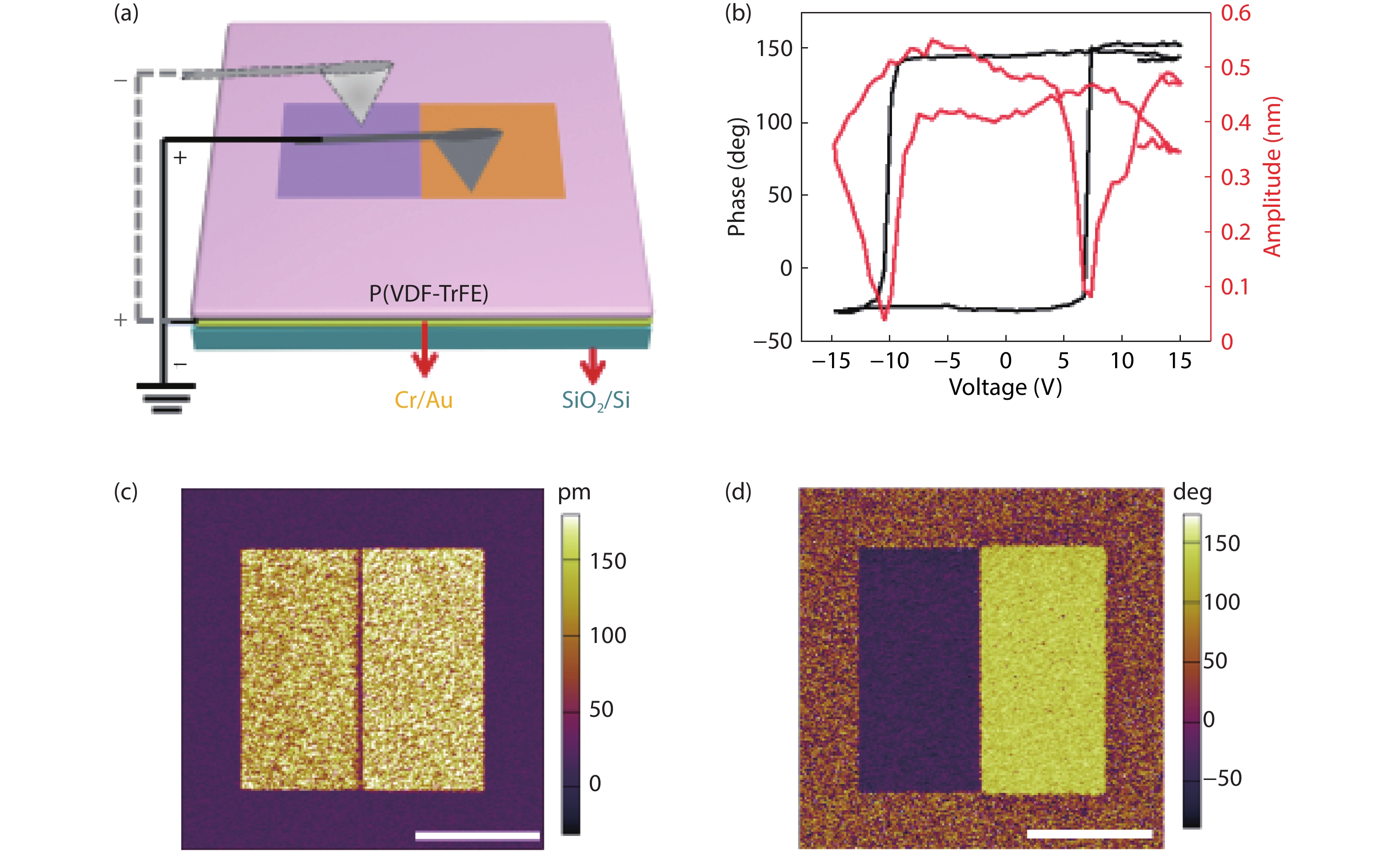
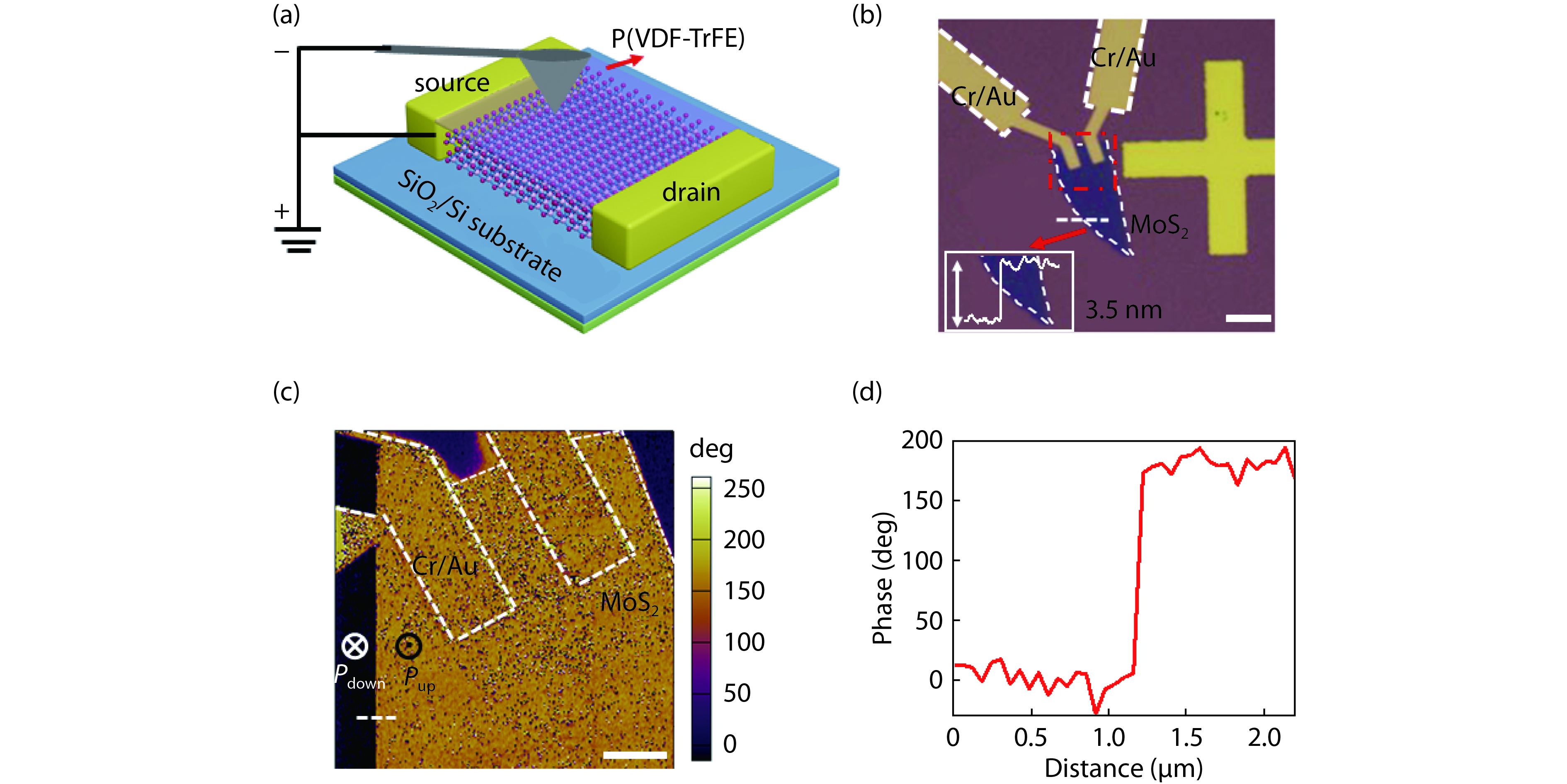
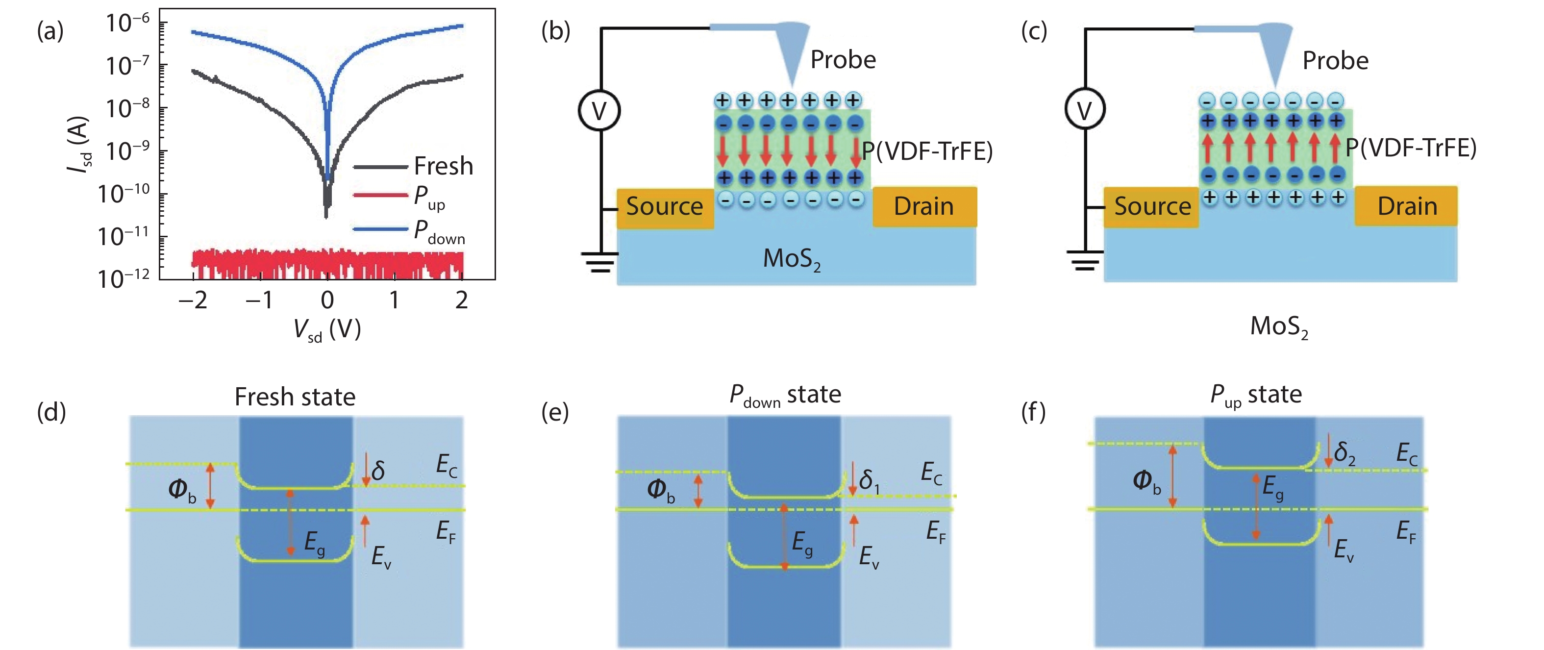
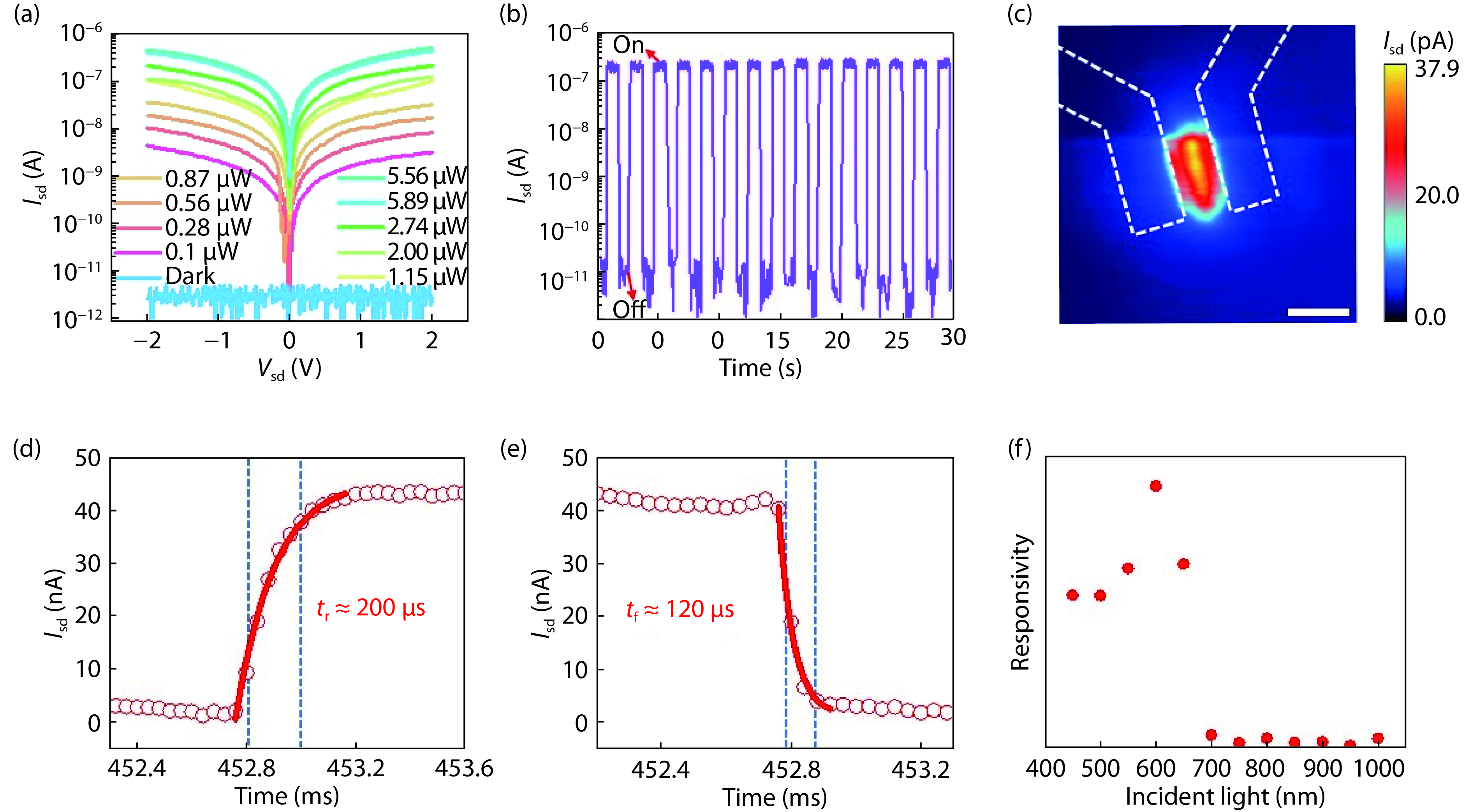
During the past decades, transition metal dichalcogenides (TMDs) have received special focus for their unique properties in photoelectric detection. As one important member of TMDs, MoS2 has been made into photodetector purely or combined with other materials, such as graphene, ionic liquid, and ferroelectric materials. Here, we report a gate-free MoS2 phototransistor combined with organic ferroelectric material poly(vinylidene fluoride-trifluoroethylene) (P(VDF-TrFE)). In this device, the remnant polarization field in P(VDF-TrFE) is obtained from the piezoelectric force microscope (PFM) probe with a positive or negative bias, which can turn the dipoles from disorder to be the same direction. Then, the MoS2 channel can be maintained at an accumulated state with downward polarization field modulation and a depleted state with upward polarization field modulation. Moreover, the P(VDF-TrFE) segregates MoS2 from oxygen and water molecules around surroundings, which enables a cleaner surface state. As a photodetector, an ultra-low dark current of 10–11 A, on/off ration of more than 104 and a fast photoresponse time of 120 μs are achieved. This work provides a new method to make high-performance phototransistors assisted by the ferroelectric domain which can operate without a gate electrode and demonstrates great potential for ultra-low power consumption applications.-
Keywords:
- TMDs,
- MoS2 phototransistor,
- P(VDF-TrFE),
- PFM,
- ultra-low power consumption
-
References
[1] Wang J. A novel spin-FET based on 2D antiferromagnet. J Semicond, 2019, 40(2), 020401 doi: 10.1088/1674-4926/40/2/020401[2] Jiang W, Wang X, Chen Y, et al. Large-area high quality PtSe2 thin film with versatile polarity. InfoMat, 2019, 1, 260 doi: 10.1002/inf2.12013[3] Wu G, Wang X, Chen Y, et al. Ultrahigh photoresponsivity MoS2 photodetector with tunable photocurrent generation mechanism. Nanotechnology, 2018, 29(48), 485204 doi: 10.1088/1361-6528/aae17e[4] Liu L, Wang X, Han L, et al. Electrical characterization of MoS2 field-effect transistors with different dielectric polymer gate. AIP Adv, 2017, 7(6), 065121 doi: 10.1063/1.4991843[5] Xue S, Zhao X L, Wang J L, et al. Preparation of La0.67Ca0.23- Sr0.1MnO3 thin films with interesting electrical and magnetic properties via pulsed-laser deposition. Sci Chin Phys, Mechan, Astron, 2017, 60(2), 027521 doi: 10.1007/s11433-016-0368-6[6] Wang J, Fang H, Wang X, et al. Recent progress on localized field enhanced two-dimensional material photodetectors from ultraviolet-visible to infrared. Small, 2017, 13(35), 1700894 doi: 10.1002/smll.201700894[7] Son Y W, Cohen M L, Louie S G. Energy gaps in graphene nanoribbons. Phys Rev Lett, 2006, 97(21), 216803 doi: 10.1103/PhysRevLett.97.216803[8] Meyer J C, Geim A K, Katsnelson M I, et al. The structure of suspended graphene sheets. Nature, 2007, 446(7131), 60 doi: 10.1038/nature05545[9] Peelaers H, Van de Walle C G. Effects of strain on band structure and effective masses in MoS2. Phys Rev B, 2012, 86(24), 241401 doi: 10.1103/PhysRevB.86.241401[10] Kang D H, Kim M S, Shim J, et al. High-performance transition metal dichalcogenide photodetectors enhanced by self-assembled monolayer doping. Adv Funct Mater, 2015, 25(27), 4219 doi: 10.1002/adfm.201501170[11] Wang L, Jie J, Shao Z, et al. MoS2/Si heterojunction with vertically standing layered structure for ultrafast, high-detectivity, self-driven visible-near infrared photodetectors. Adv Funct Maters, 2015, 25(19), 2910 doi: 10.1002/adfm.201500216[12] Jariwala D, Sangwan V K, Wu C C, et al. Gate-tunable carbon nanotube-MoS2 heterojunction pn diode. Proc Nat Acad Sci, 2013, 110(45), 18076 doi: 10.1073/pnas.1317226110[13] Novoselov K S, Geim A K, Morozov S V, et al. Electric field effect in atomically thin carbon films. Science, 2004, 306(5696), 666 doi: 10.1126/science.1102896[14] Addou R, Colombo L, Wallace R M. Surface defects on natural MoS2. ACS Appl Mater Interfaces, 2015, 7(22), 11921 doi: 10.1021/acsami.5b01778[15] Di Bartolomeo A, Genovese L, Giubileo F, et al. Hysteresis in the transfer characteristics of MoS2 transistors. 2D Mater, 2017, 5(1), 015014 doi: 10.1088/2053-1583/aa91a7[16] Kwon J, Hong Y K, Han G, et al. Giant photoamplification in indirect-bandgap multilayer MoS2 phototransistors with local bottom-gate structures. Adv Mater, 2015, 27(13), 2224 doi: 10.1002/adma.201404367[17] Zhang W, Huang J K, Chen C H, et al. High-gain phototransistors based on a CVD MoS2 monolayer. Adv Mater, 2013, 25(25), 3456 doi: 10.1002/adma.201301244[18] Wu C L, Chen J W. Chen C H, et al. A gate-free monolayer WSe2 pn diode. APS Meeting Abstracts, 2018[19] Baeumer C, Saldana-Greco D, Martirez J M P, et al. Ferroelectrically driven spatial carrier density modulation in graphene. Nat Commun, 2015, 6, 6136 doi: 10.1038/ncomms7136[20] Yin C, Wang X, Chen Y, et al. A ferroelectric relaxor polymer-enhanced p-type WSe2 transistor. Nanoscale, 2018, 10(4), 1727 doi: 10.1039/C7NR08034D[21] Tian B B, Wang J L, Fusil S, et al. Tunnel electroresistance through organic ferroelectrics. Nat Commun, 2016, 7, 11502 doi: 10.1038/ncomms11502[22] Wang X, Wang P, Wang J, et al. Ultrasensitive and broadband MoS2 photodetector driven by ferroelectrics. Adv Mater, 2015, 27(42), 6575 doi: 10.1002/adma.201503340[23] Kufer D, Konstantatos G. Highly sensitive, encapsulated MoS2 photodetector with gate controllable gain and speed. Nano Lett, 2015, 15(11), 7307 doi: 10.1021/acs.nanolett.5b02559[24] Lee H S, Min S W, Park M K, et al. MoS2 nanosheets for top-gate nonvolatile memory transistor channel. Small, 2012, 8(20), 3111 doi: 10.1002/smll.201200752[25] Zhang E, Wang W, Zhang C, et al. Tunable charge-trap memory based on few-layer MoS2. ACS Nano, 2014, 9(1), 612 doi: 10.1021/nn5059419[26] Zhao D, Katsouras I, Asadi K, et al. Switching dynamics in ferroelectric P (VDF-TrFE) thin films. Phys Rev B, 2015, 92(21), 214115 doi: 10.1103/PhysRevB.92.214115[27] Furchi M M, Polyushkin D K, Pospischil A, et al. Mechanisms of photoconductivity in atomically thin MoS2. Nano Lett, 2014, 14(11), 6165 doi: 10.1021/nl502339q[28] Lee H S, Min S W, Chang Y G, et al. MoS2 nanosheet phototransistors with thickness-modulated optical energy gap. Nano Lett, 2012, 12(7), 3695 doi: 10.1021/nl301485q[29] Li H, Wu J, Yin Z, et al. Preparation and applications of mechanically exfoliated single-layer and multilayer MoS2 and WSe2 nanosheets. Acc Chem Res, 2014, 47(4), 1067 doi: 10.1021/ar4002312[30] Gruverman A, Kalinin S V. Piezoresponse force microscopy and recent advances in nanoscale studies of ferroelectrics. J Mater Sci, 2006, 41(1), 107 doi: 10.1007/s10853-005-5946-0[31] Chen X, Wu Z, Xu S, et al. Probing the electron states and metal-insulator transition mechanisms in molybdenum disulphide vertical heterostructures. Nat Commun, 2015, 6, 6088 doi: 10.1038/ncomms7088[32] Santos E J G, Kaxiras E. Electrically driven tuning of the dielectric constant in MoS2 layers. ACS Nano, 2013, 7(12), 10741 doi: 10.1021/nn403738b[33] Xie Y, Zhang B, Wang S, et al. Ultrabroadband MoS2 photodetector with spectral response from 445 to 2717 nm. Adv Mater, 2017, 29(17), 1605972 doi: 10.1002/adma.201605972[34] Lopez-Sanchez O, Lembke D, Kayci M, et al. Ultrasensitive photodetectors based on monolayer MoS2. Nat Nanotechnol, 2013, 8(7), 497 doi: 10.1038/nnano.2013.100[35] McCreary K M, Hanbicki A T, Robinson J T, et al. Large-area synthesis of continuous and uniform MoS2 monolayer films on graphene. Adv Funct Mater, 2014, 24(41), 6449 doi: 10.1002/adfm.201401511[36] Long M, Wang P, Fang H, et al. Progress, challenges, and opportunities for 2D material based photodetectors. Adv Funct Mater, 2019, 29(19), 1803807 doi: 10.1002/adfm.201803807[37] Yin L, Wang Z, Wang F, et al. Ferroelectric-induced carrier modulation for ambipolar transition metal dichalcogenide transistors. Appl Phys Lett, 2017, 110(12) doi: 10.1063/1.4979088[38] Choi W, Cho M Y, Konar A, et al. High-detectivity multilayer MoS2 phototransistors with spectral response from ultraviolet to infrared. Adv Mater, 2012, 24(43), 5832 doi: 10.1002/adma.201201909 -
Supplements
 19070020suppl.pdf

-
Proportional views


 DownLoad:


