| Citation: |
H. Zandipour, M. Madani. Design, modelling, and simulation of a floating gate transistor with a novel security feature[J]. Journal of Semiconductors, 2020, 41(10): 102105. doi: 10.1088/1674-4926/41/10/102105
****
H Zandipour, M Madani, Design, modelling, and simulation of a floating gate transistor with a novel security feature[J]. J. Semicond., 2020, 41(10): 102105. doi: 10.1088/1674-4926/41/10/102105.
|
Design, modelling, and simulation of a floating gate transistor with a novel security feature
DOI: 10.1088/1674-4926/41/10/102105
More Information
-
Abstract
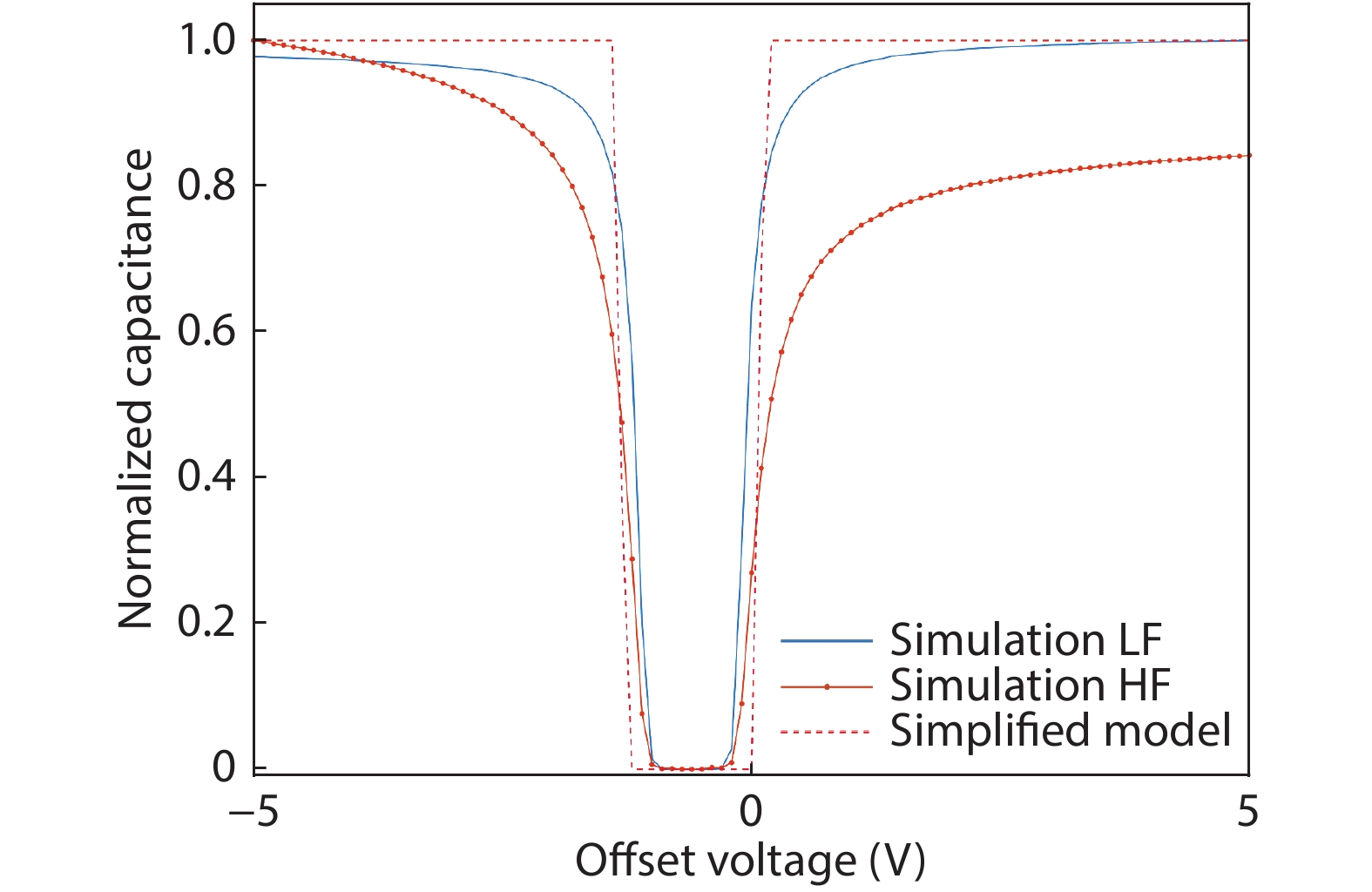
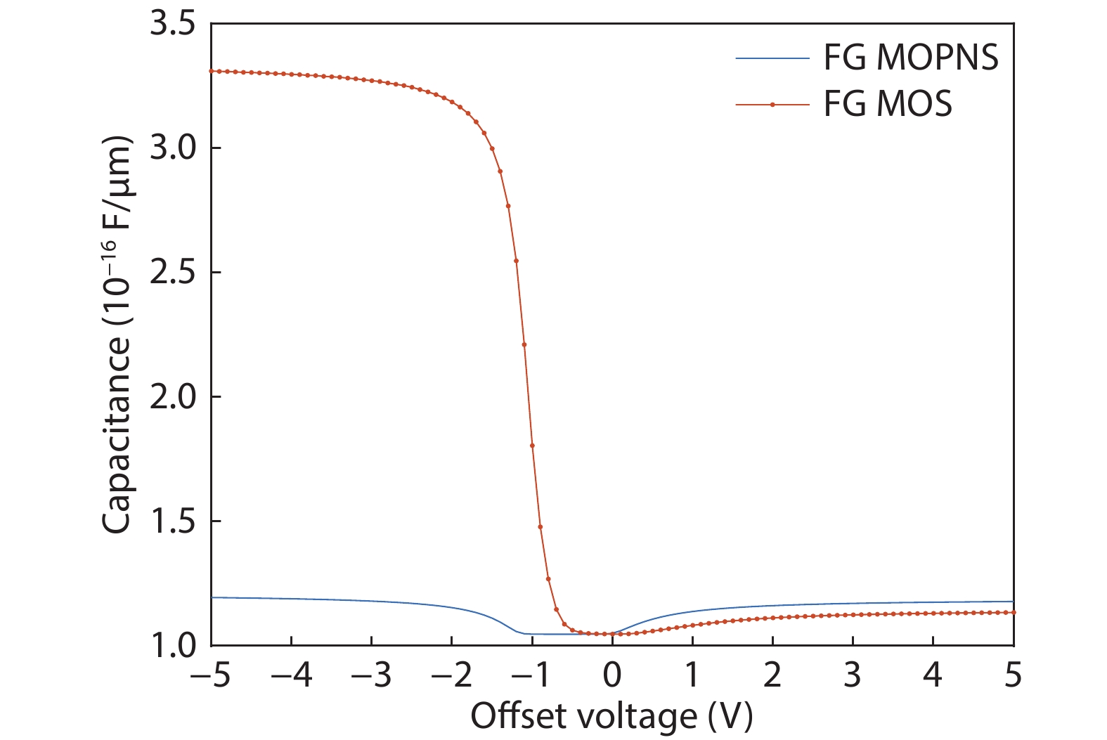
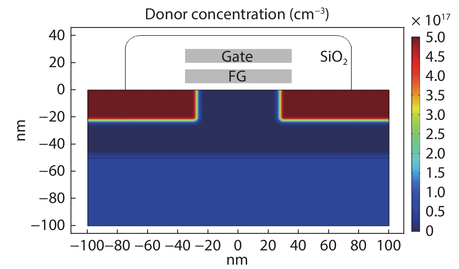
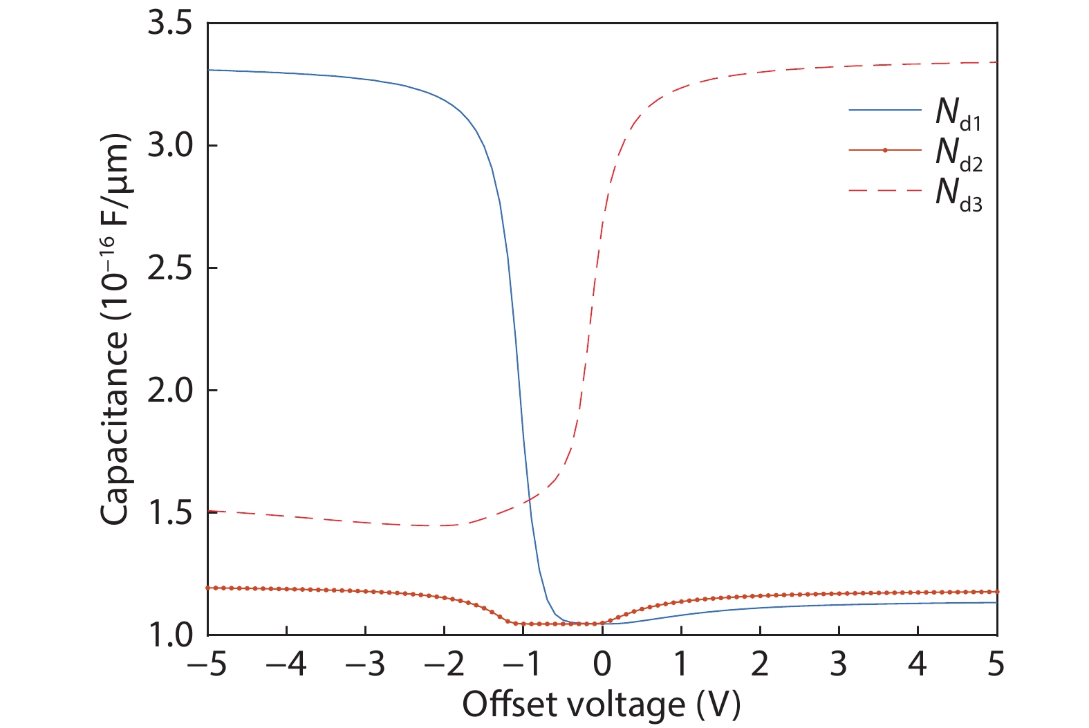
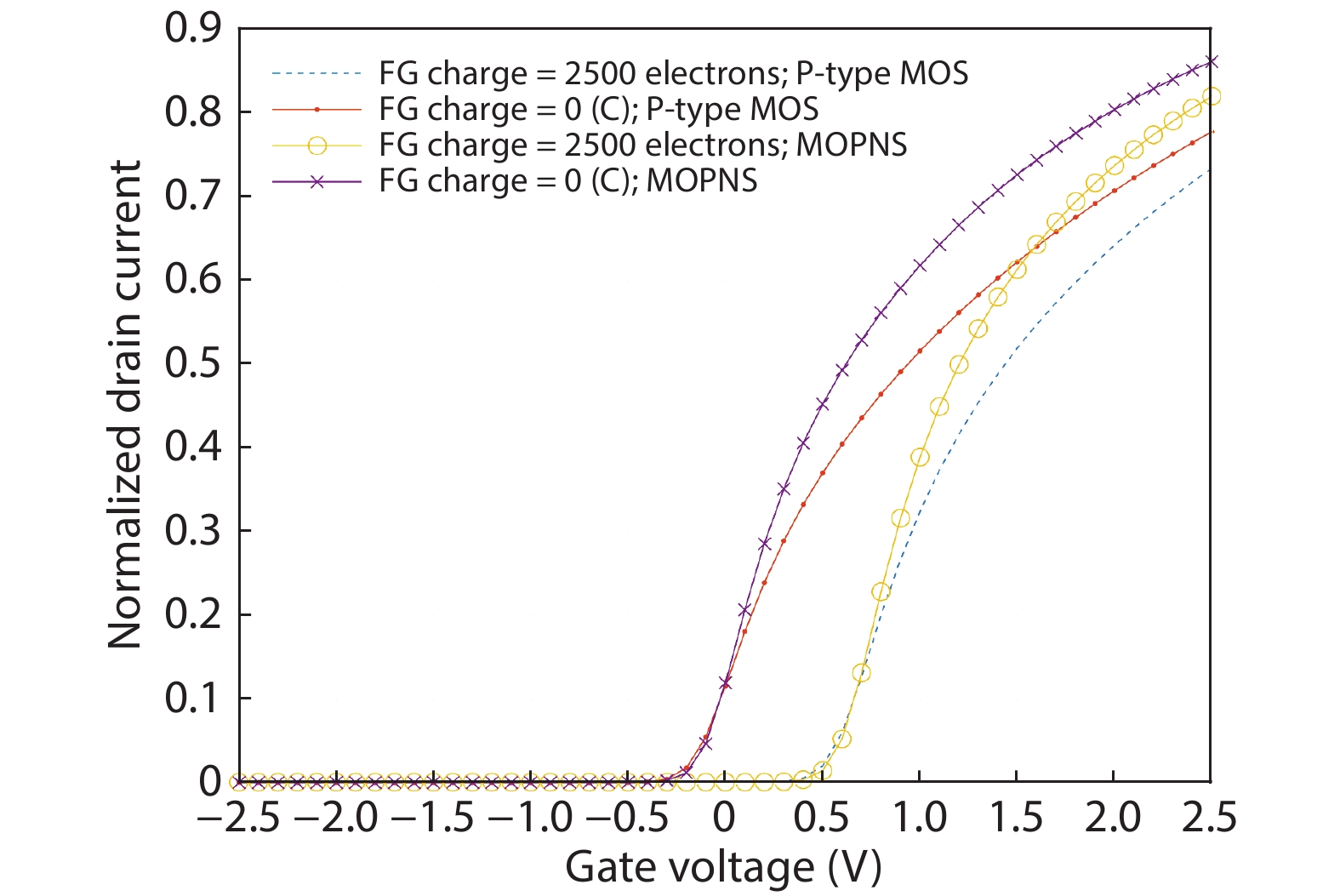
This study proposes a new generation of floating gate transistors (FGT) with a novel built-in security feature. The new device has applications in guarding the IC chips against the current reverse engineering techniques, including scanning capacitance microscopy (SCM). The SCM measures the change in the C–V characteristic of the device as a result of placing a minute amount of charge on the floating gate, even in nano-meter scales. The proposed design only adds a simple processing step to the conventional FGT by adding an oppositely doped implanted layer to the substrate. This new structure was first analyzed theoretically and then a two-dimensional model was extracted to represent its C–V characteristic. Furthermore, this model was verified with a simulation. In addition, the C–V characteristics relevant to the SCM measurement of both conventional and the new designed FGT were compared to discuss the effectiveness of the added layer in masking the state of the transistor. The effect of change in doping concentration of the implanted layer on the C–V characteristics was also investigated. Finally, the feasibility of the proposed design was examined by comparing its I–V characteristics with the traditional FGT. -
References
[1] Fujita O, Amemiya Y. A floating-gate analog memory device for neural networks. IEEE Trans Electron Devices, 1993, 40, 2029 doi: 10.1109/16.239745[2] Wang G, Liu X, Wang W. Solution processed organic transistor nonvolatile memory with a floating-gate of carbon nanotubes. IEEE Electron Device Lett, 2018, 39, 111 doi: 10.1109/LED.2017.2774826[3] Jia X, Feng P, Zhang S, et al. An ultra-low-power area-efficient non-volatile memory in a 0.18 μm single-poly CMOS process for passive RFID tags. J Semicond, 2013, 34, 085004 doi: 10.1088/1674-4926/34/8/085004[4] Lee J, Jeong Y, Jeong H, et al. Fabrication and characterization of a new EEPROM cell with spacer select transistor. IEEE Electron Device Lett, 2005, 26, 569 doi: 10.1109/LED.2005.852541[5] Fang L, Kong W, Gu J, et al. A novel symmetrical split-gate structure for 2-bit per cell flash memory. J Semicond, 2014, 35, 074008 doi: 10.1088/1674-4926/35/7/074008[6] Cacharelis P, Fong E, Torgerson E, et al. A single transistor electrically alterable cell. IEEE Electron Device Lett, 1985, 6, 519 doi: 10.1109/EDL.1985.26215[7] Dimaria D, Demeyer K, Dong D. Electrically-alterable memory using a dual electron injector structure. IEEE Electron Device Lett, 1980, 1, 179 doi: 10.1109/EDL.1980.25279[8] Wu J, Zhang L Q, Yao Y, et al. Investigation of dynamic threshold voltage behavior in semi-floating gate transistor for normally-off AlGaN/GaN HEMT. IEEE J Electron Devices Soc, 2017, 5, 117 doi: 10.1109/JEDS.2017.2647979[9] Kim Y M, Kim S J, Lee J S. Organic-transistor-based nano-floating-gate memory devices having multistack charge-trapping layers. IEEE Electron Device Lett, 2010, 31, 503 doi: 10.1109/LED.2010.2041743[10] Schauer H, Tran L V, Smith L. A high-density, high-performance EEPROM cell. IEEE Trans Electron Devices, 1982, 29, 1178 doi: 10.1109/T-ED.1982.20854[11] Kolodny A, Nieh S, Eitan B, et al. Analysis and modeling of floating-gate EEPROM cells. IEEE Trans Electron Devices, 1986, 33, 835 doi: 10.1109/T-ED.1986.22576[12] Holler M, Guizar-Sicairos M, Tsai E H R, et al. High-resolution non-destructive three-dimensional imaging of integrated circuits. Nature, 2017, 543, 402 doi: 10.1038/nature21698[13] Quadir S E, Chen J, Forte D, et al. A survey on chip to system reverse engineering ACM. J Emerg Technol Comput Syst, 2016, 13, 1 doi: 10.1145/2755563[14] Henning A K, Hochwitz T, Slinkman J, et al. Two-dimensional surface dopant profiling in silicon using scanning Kelvin probe microscopy. J Appl Phys, 1995, 77, 1888 doi: 10.1063/1.358819[15] Bidani L, Baharav O, Sinvani M, et al. Usage of laser timing probe for sensing of programmed charges in EEPROM devices. IEEE Trans Device Mater Reliab, 2014, 14, 304 doi: 10.1109/TDMR.2013.2272218[16] Matey J R. Scanning capacitance microscopy. Scan Microscopy Technol Appl, 1988, 897, 110[17] Denardi C, Desplats R, Perdu P, et al. Descrambling and data reading techniques for flash-EEPROM memories. Application smart cards. Microelectron Reliab, 2006, 46, 1569 doi: 10.1016/j.microrel.2006.07.022 -
Proportional views


 DownLoad:
