| [1] |
Choi K J, Biegalski M, Li Y L, et al. Enhancement of ferroelectricity in strained BaTiO 3 thin films. Science, 2004, 306(5698), 1005 doi: 10.1126/science.1103218 |
| [2] |
Wang C, Ke X, Wang J, et al. Ferroelastic switching in a layered-perovskite thin film. Nat Commun, 2016, 7, 10636 doi: 10.1038/ncomms10636 |
| [3] |
Lan H, Liang F, Jiang X, et al. Pushing nonlinear optical oxides into the mid-infrared spectral region beyond 10 μm: design, synthesis, and characterization of La 3SnGa 5O 14. J Am Chem Soc, 2018, 140(13), 4684 doi: 10.1021/jacs.8b01009 |
| [4] |
Chen Z, Chen Z, Kuo C Y, et al. Complex strain evolution of polar and magnetic order in multiferroic BiFeO 3 thin films. Nat Commun, 2018, 9, 3764 doi: 10.1038/s41467-018-06190-5 |
| [5] |
Himcinschi C, Rix J, Röder C, et al. Ferroelastic domain identification in BiFeO 3 crystals using Raman spectroscopy. Sci Rep, 2019, 9, 379 doi: 10.1038/s41598-018-36462-5 |
| [6] |
Lin Y, Feng D Y, Gao M, et al. Reducing dielectric loss in CaCu 3Ti 4O 12 thin films by high-pressure oxygen annealing. J Mater Chem C, 2015, 3(14), 3438 doi: 10.1039/C5TC00197H |
| [7] |
Yao G, Gao M, Ji Y, et al. Surface step terrace tuned microstructures and dielectric properties of highly epitaxial CaCu 3Ti 4O 12 thin films on vicinal LaAlO 3 substrates. Sci Rep, 2016, 6, 34683 doi: 10.1038/srep34683 |
| [8] |
Yao G, Ji Y, Liang W, et al. Influence of vicinal surface on the anisotropic dielectric properties of highly epitaxial Ba 0.7Sr 0.3TiO 3 thin films. Nanoscale, 2017, 9(9), 3068 doi: 10.1039/C6NR09044C |
| [9] |
Choi M C, Kim Y, Ha C S. Polymers for flexible displays: from material selection to device applications. Prog Polym Sci, 2008, 33(6), 581 doi: 10.1016/j.progpolymsci.2007.11.004 |
| [10] |
Jiang J, Bitla Y, Huang C W, et al. Flexible ferroelectric element based on van der Waals heteroepitaxy. Sci Adv, 2017, 3(6), e1700121 doi: 10.1126/sciadv.1700121 |
| [11] |
Ahn J H, Kim H S, Lee K J, et al. Heterogeneous three-dimensional electronics by use of printed semiconductor nanomaterials. Science, 2006, 314(5806), 1754 doi: 10.1126/science.1132394 |
| [12] |
Yao G, Jiang D, Li J, et al. Self-activated electrical stimulation for effective hair regeneration via a wearable omnidirectional pulse generator. ACS Nano, 2019, 13(11), 12345 doi: 10.1021/acsnano.9b03912 |
| [13] |
Yao G, Kang L, Li J, et al. Effective weight control via an implanted self-powered vagus nerve stimulation device. Nat Commun, 2018, 9, 5349 doi: 10.1038/s41467-018-07764-z |
| [14] |
Yao G, Zhang H, Zhang S, et al. Highly sensitive pressure switch sensors and enhanced near ultraviolet photodetectors based on 3D hybrid film of graphene sheets decorated with silver nanoparticles. RSC Adv, 2017, 7(44), 27281 doi: 10.1039/C7RA02342A |
| [15] |
Zhang S, Zhang H, Yao G, et al. Highly stretchable, sensitive, and flexible strain sensors based on silver nanoparticles/carbon nanotubes composites. J Alloys Compd, 2015, 652, 48 doi: 10.1016/j.jallcom.2015.08.187 |
| [16] |
Kim D H, Song J, Choi W M, et al. Materials and noncoplanar mesh designs for integrated circuits with linear elastic responses to extreme mechanical deformations. Proc Natl Acad Sci USA, 2008, 105(48), 18675 doi: 10.1073/pnas.0807476105 |
| [17] |
Kim R H, Kim D H, Xiao J, et al. Waterproof AlInGaP optoelectronics on stretchable substrates with applications in biomedicine and robotics. Nat Mater, 2010, 9(11), 929 doi: 10.1038/nmat2879 |
| [18] |
Khang D Y, Jiang H, Huang Y, et al. A stretchable form of single-crystal silicon for high-performance electronics on rubber substrates. Science, 2006, 311(5758), 208 doi: 10.1126/science.1121401 |
| [19] |
Ko H C, Shin G, Wang S, et al. Curvilinear electronics formed using silicon membrane circuits and elastomeric transfer elements. Small, 2009, 5(23), 2703 doi: 10.1002/smll.200900934 |
| [20] |
Mohan A M V, Kim N H, Gu Y, et al. Merging of thin- and thick-film fabrication technologies: toward soft stretchable “island-bridge” devices. Adv Mater Technol, 2017, 2(4), 1600284 doi: 10.1002/admt.201600284 |
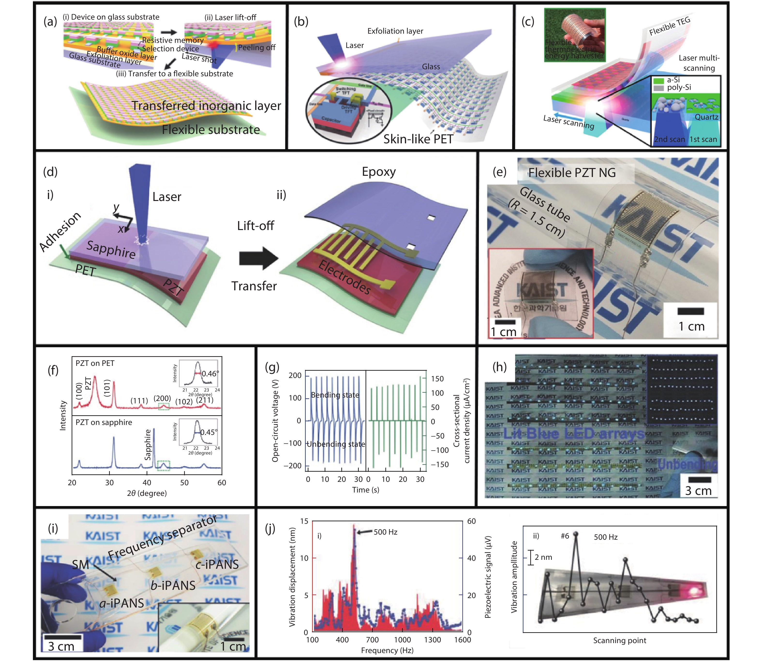
| [21] |
Xu S, Zhang Y, Jia L, et al. Soft microfluidic assemblies of sensors, circuits, and radios for the skin. Science, 2014, 344(6179), 70 doi: 10.1126/science.1250169 |
| [22] |
Huang Z, Hao Y, Li Y, et al. Three-dimensional integrated stretchable electronics. Nat Electron, 2018, 1(8), 473 doi: 10.1038/s41928-018-0116-y |
| [23] |
Jang K I, Li K, Chung H U, et al. Self-assembled three dimensional network designs for soft electronics. Nat Commun, 2017, 8, 15894 doi: 10.1038/ncomms15894 |
| [24] |
Wong W S, Sands T, Cheung N W, et al. Fabrication of thin-film InGaN light-emitting diode membranes by laser lift-off. Appl Phys Lett, 1999, 75(10), 1360 doi: 10.1063/1.124693 |
| [25] |
Fujii T, David A, Schwach C, et al. Micro cavity effect in GaN-based light-emitting diodes formed by laser lift-off and etch-back technique. Jpn J Appl Phys, 2004, 43(3B), L411 doi: 10.1143/jjap.43.l411 |
| [26] |
Chu C F, Lai F I, Chu J T, et al. Study of GaN light-emitting diodes fabricated by laser lift-off technique. J Appl Phys, 2004, 95(8), 3916 doi: 10.1063/1.1651338 |
| [27] |
Li C I, Lin J C, Liu H J, et al. Van der Waal epitaxy of flexible and transparent VO 2 film on muscovite. Chem Mater, 2016, 28(11), 3914 doi: 10.1021/acs.chemmater.6b01180 |
| [28] |
Utama M I B, Mata M D L, Magen C, et al. Twinning-, polytypism-, and polarity-induced morphological modulation in nonplanar nanostructures with van der Waals epitaxy. Adv Funct Mater, 2013, 23(13), 1636 doi: 10.1002/adfm.201202027 |
| [29] |
Ma C H, Lin J C, Liu H J, et al. Van der Waals epitaxy of functional MoO 2 film on mica for flexible electronics. Appl Phys Lett, 2016, 108(25), 253104 doi: 10.1063/1.4954172 |
| [30] |
Wong W S, Sands T, Cheung N W, et al. Damage-free separation of GaN thin films from sapphire substrates. Appl Phys Lett, 1998, 72(5), 599 doi: 10.1063/1.120816 |
| [31] |
Luo J, Pohl R, Qi L, et al. Printing functional 3D microdevices by laser-induced forward transfer. Small, 2017, 13(9), 1602553 doi: 10.1002/smll.201602553 |
| [32] |
Serra P, Piqué A. Laser-induced forward transfer: fundamentals and applications. Adv Mater Technol, 2018, 4(1), 1800099 doi: 10.1002/admt.201800099 |
| [33] |
Fernández-Pradas J M, Sopeña P, González-Torres S, et al. Laser-induced forward transfer for printed electronics applications. Appl Phys A, 2018, 124(2), 214 doi: 10.1007/s00339-018-1648-8 |
| [34] |
Sorkio A, Koch L, Koivusalo L, et al. Human stem cell based corneal tissue mimicking structures using laser-assisted 3D bioprinting and functional bioinks. Biomaterials, 2018, 171, 57 doi: 10.1016/j.biomaterials.2018.04.034 |
| [35] |
Kérourédan O, Ribot E, Fricain J, et al. Magnetic resonance imaging for tracking cellular patterns obtained by laser-assisted bioprinting. Sci Rep, 2018, 8, 15777 doi: 10.1038/s41598-018-34226-9 |
| [36] |
Koch L, Brandt O, Deiwick A, et al. Laser-assisted bioprinting: a novel approach for bone regeneration application. Med Sci, 2018, 34(2), 125 doi: 10.1051/medsci/20183402008 |
| [37] |
Keriquel V, Oliveira H, Rémy M, et al. In situ printing of mesenchymal stromal cells, by laser-assisted bioprinting, for in vivo bone regeneration applications. Sci Rep, 2017, 7(1), 1778 doi: 10.1038/s41598-017-01914-x |
| [38] |
Gao Y, Li Y, Li R, et al. An accurate thermomechanical model for laser-driven microtransfer printing. J Appl Mech-T ASME, 2017, 84(6), 064501 doi: 10.1115/1.4036257 |
| [39] |
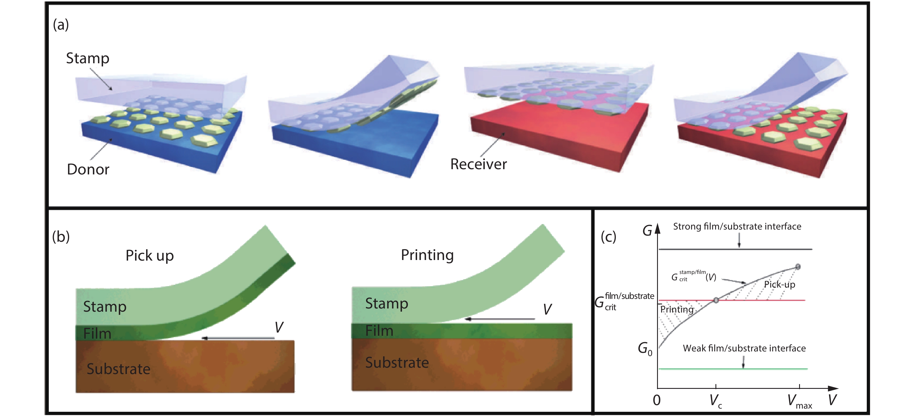
Luo H, Wang C, Linghu C, et al. Laser-driven programmable non-contact transfer printing of objects onto arbitrary receivers via an active elastomeric micro-structured stamp. Natl Sci Rev, 2019, 7, 296 doi: 10.1093/nsr/nwz109 |
| [40] |
Kim S, Son J H, Lee S H, et al. Flexible crossbar-structured resistive memory arrays on plastic substrates via inorganic-based laser lift-off. Adv Mater, 2014, 26(44), 7480 doi: 10.1002/adma.201402472 |
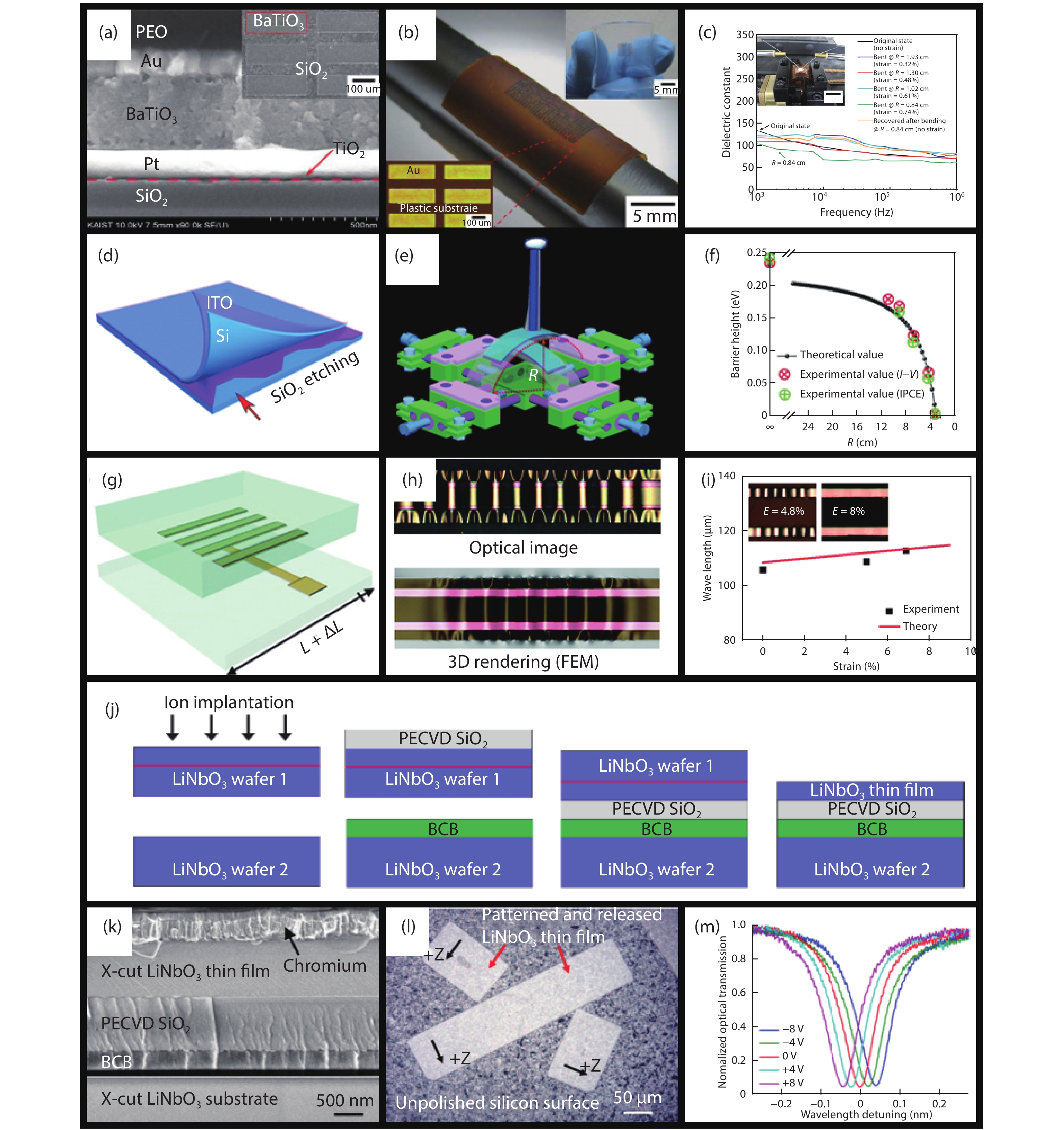
| [41] |
Lee H E, Kim S, Ko J, et al. Skin-like oxide thin-film transistors for transparent displays. Adv Funct Mater, 2016, 26(34), 6170 doi: 10.1002/adfm.201601296 |
| [42] |
Cheung Y F, Li K H, Choi H W, et al. Flexible free-standing III-nitride thin films for emitters and displays. ACS Appl Mater Interfaces, 2016, 8(33), 21440 doi: 10.1021/acsami.6b04413 |
| [43] |
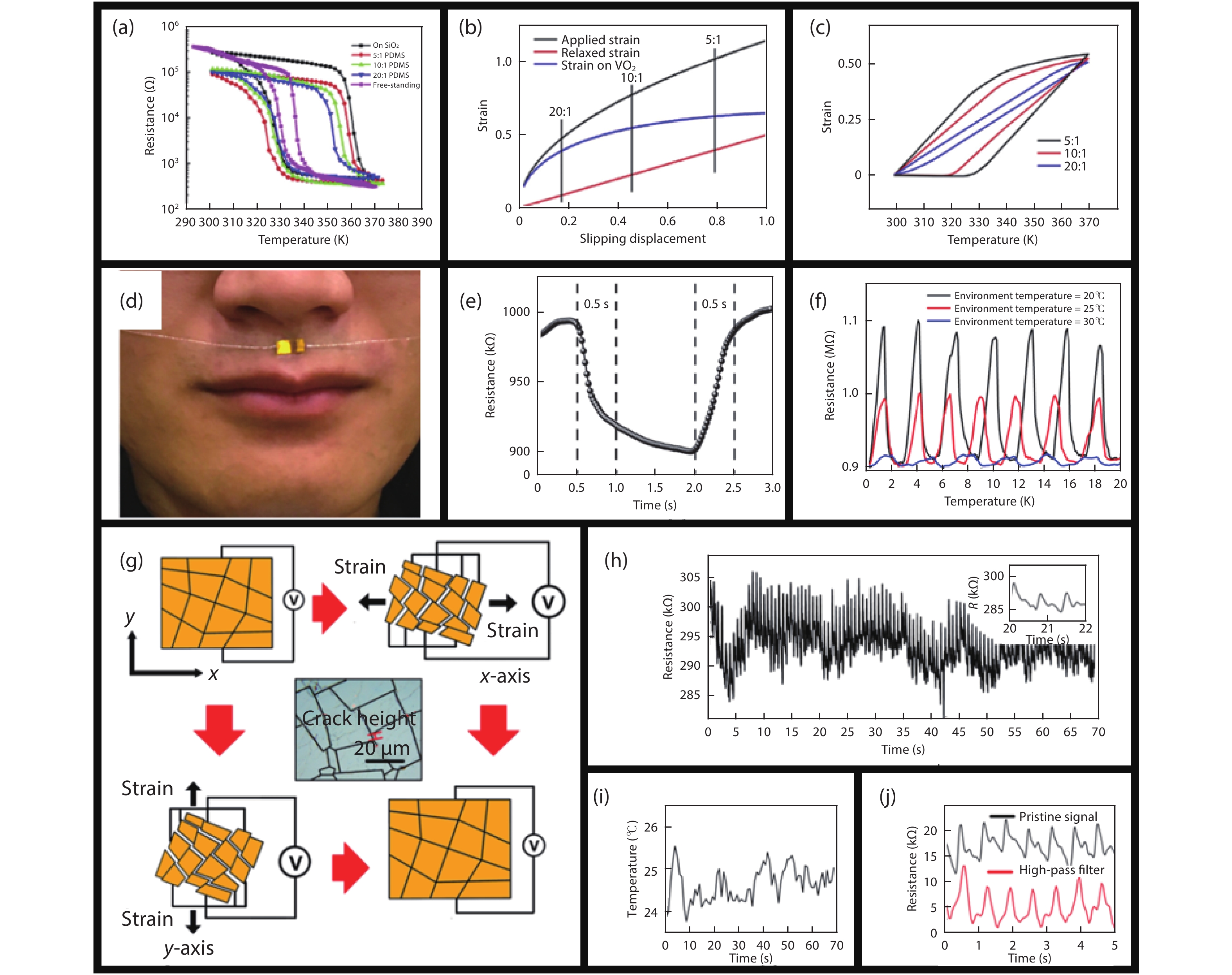
Kim T I, Jung Y H, Song J, et al. High-efficiency, microscale GaN light-emitting diodes and their thermal properties on unusual substrates. Small, 2012, 8(11), 1643 doi: 10.1002/smll.201200382 |
| [44] |
Lee H E, Choi J, Lee S H, et al. Monolithic flexible vertical GaN light-emitting diodes for a transparent wireless brain optical stimulator. Adv Mater, 2018, 30(28), e1800649 doi: 10.1002/adma.201800649 |
| [45] |
Kim S J, Lee H E, Choi H, et al. High-performance flexible thermoelectric power generator using laser multiscanning lift-off process. ACS Nano, 2016, 10(12), 10851 doi: 10.1021/acsnano.6b05004 |
| [46] |
Park K I, Son J H, Hwang G T, et al. Highly-efficient, flexible piezoelectric PZT thin film nanogenerator on plastic substrates. Adv Mater, 2014, 26(16), 2514 doi: 10.1002/adma.201305659 |
| [47] |
Lee H S, Chung J, Hwang G T, et al. Flexible inorganic piezoelectric acoustic nanosensors for biomimetic artificial hair cells. Adv Funct Mater, 2014, 24(44), 6914 doi: 10.1002/adfm.201402270 |
| [48] |
Mendes M, Fu J, Porneala C, et al. Lasers in the manufacturing of LEDs. Proc SPIE, 2010, 7584, 75840T doi: 10.1117/12.843815 |
| [49] |
Chuang S H, Pan C T, Shen K C, et al. Thin film GaN LEDs using a patterned oxide sacrificial layer by chemical lift-off process. IEEE Photonics Technol Lett, 2013, 25(24), 2435 doi: 10.1109/LPT.2013.2287892 |
| [50] |
Morimoto A, Tanimura H, Yang H, et al. Platinum film patterning by laser lift-off using hydrocarbon film on insulating substrates. Appl Phys A, 2004, 79(4–6), 1015 doi: 10.1007/s00339-004-2617-y |
| [51] |
Palneedi H, Park J H, Maurya D, et al. Laser irradiation of metal oxide films and nanostructures: applications and advances. Adv Mater, 2018, 30(14), e1705148 doi: 10.1002/adma.201705148 |
| [52] |
Xu X, Liu W, Li Y, et al. Flexible mica films for high-temperature energy storage. J Materiom, 2018, 4(3), 173 doi: 10.1016/j.jmat.2018.04.003 |
| [53] |
Ohta S I. Synthetic mica and its applications. Clay Sci, 2006, 12, 119
|
| [54] |
Shen L, Liu M, Ma C, et al. Enhanced bending tuned magnetic properties in epitaxial cobalt ferrite nanopillar arrays on flexible substrate. Mater Horiz, 2018, 5(2), 230 doi: 10.1039/C7MH00939A |
| [55] |
Gao D, Tan Z, Fan Z, et al. All-inorganic flexible Ba 0.67Sr 0.33TiO 3 thin films with excellent dielectric properties over a wide range of frequencies. ACS Appl Mater Interfaces, 2019, 11(30), 27088 doi: 10.1021/acsami.9b08712 |
| [56] |
Tsai M F, Jiang J, Shao P W, et al. Oxide heteroepitaxy based flexible ferroelectric transistor. ACS Appl Mater Interfaces, 2019, 11(29), 25882 doi: 10.1021/acsami.9b06332 |
| [57] |
Quynh L T, Van C N, Tzeng W Y, et al. Flexible heteroepitaxy photoelectrode for photo-electrochemical water splitting. ACS Appl Energy Mater, 2018, 1(8), 3900 doi: 10.1021/acsaem.8b00645 |
| [58] |
Liu H J, Wang C K, Su D, et al. Flexible heteroepitaxy of CoFe 2O 4/muscovite bimorph with large magnetostriction. ACS Appl Mater Interfaces, 2017, 9(8), 7297 doi: 10.1021/acsami.6b16485 |
| [59] |
Wu P C, Chen P F, Do T H, et al. Heteroepitaxy of Fe 3O 4/muscovite: a new perspective for flexible spintronics. ACS Appl Mater Interfaces, 2016, 8(49), 33794 doi: 10.1021/acsami.6b11610 |
| [60] |
Hou W, Zhou Z, Zhang L, et al. Low-voltage-manipulating spin dynamics of flexible Fe 3O 4 films through ionic gel gating for wearable devices. ACS Appl Mater Interfaces, 2019, 11(24), 21727 doi: 10.1021/acsami.9b06505 |
| [61] |
Liu W, Ma R, Liu M, et al. Highly stable in-plane microwave magnetism in flexible Li 0.35Zn 0.3Fe 2.35O 4 (111) epitaxial thin films for wearable devices. ACS Appl Mater Interfaces, 2018, 10(38), 32331 doi: 10.1021/acsami.8b09984 |
| [62] |
Liu W, Liu M, Ma R, et al. Mechanical strain-tunable microwave magnetism in flexible CuFe 2O 4 epitaxial thin film for wearable sensors. Adv Funct Mater, 2018, 28(10), 1705928 doi: 10.1002/adfm.201705928 |
| [63] |
Amrillah T, Bitla Y, Shin K, et al. Flexible multiferroic bulk heterojunction with giant magnetoelectric coupling via the van der Waals epitaxy. ACS Nano, 2017, 11(6), 6122 doi: 10.1021/acsnano.7b02102 |
| [64] |
Yang Y, Yuan G, Yan Z, et al. Flexible, semitransparent, and inorganic resistive memory based on BaTi 0.95Co 0.05O 3 film. Adv Mater, 2017, 29(26), 1700425 doi: 10.1002/adma.201700425 |
| [65] |
Gao W, You L, Wang Y, et al. Flexible PbZr 0.52Ti 0.48O 3 capacitors with giant piezoelectric response and dielectric tunability. Adv Electron Mater, 2017, 3(8), 1600542 doi: 10.1002/aelm.201600542 |
| [66] |
Liang Z, Ma C, Shen L, et al. Flexible lead-free oxide film capacitors with ultrahigh energy storage performances in extremely wide operating temperature. Nano Energy, 2019, 57, 519 doi: 10.1016/j.nanoen.2018.12.056 |
| [67] |
Liang Z, Liu M, Shen L, et al. All-inorganic flexible embedded thin film capacitors for dielectric energy storage with high performance. ACS Appl Mater Interfaces, 2019, 11(5), 5247 doi: 10.1021/acsami.8b18429 |
| [68] |
Wu J, Liang Z, Ma C, et al. Flexible lead-free BaTiO 3 ferroelectric elements with high performance. IEEE Electron Device Lett, 2019, 40(6), 889 doi: 10.1109/LED.2019.2911956 |
| [69] |
Wu P C, Lin Y P, Juan Y H, et al. Epitaxial yttria-stabilized zirconia on muscovite for flexible transparent ionic conductors. ACS Appl Nano Mater, 2018, 1(12), 6890 doi: 10.1021/acsanm.8b01698 |
| [70] |
Bitla Y, Chen C, Lee H C, et al. Oxide heteroepitaxy for flexible optoelectronics. ACS Appl Mater Interfaces, 2016, 8(47), 32401 doi: 10.1021/acsami.6b10631 |
| [71] |
Ke S, Chen C, Fu N, et al. Transparent indium tin oxide electrodes on muscovite mica for high-temperature-processed flexible optoelectronic devices. ACS Appl Mater Interfaces, 2016, 8(42), 28406 doi: 10.1021/acsami.6b09166 |
| [72] |
Li M, Wang Y, Wang Y, et al. AZO/Ag/AZO transparent flexible electrodes on mica substrates for high temperature application. Ceram Int, 2017, 43(17), 15442 doi: 10.1016/j.ceramint.2017.08.089 |
| [73] |
Yang Y, Gao W, Xie Z, et al. An all-inorganic, transparent, flexible, and nonvolatile resistive memory. Adv Electron Mater, 2018, 4(12), 1800412 doi: 10.1002/aelm.201800412 |
| [74] |
Zhang Y, Cao Y, Hu H, et al. Flexible metal-insulator transitions based on van der Waals oxide heterostructures. ACS Appl Mater Interfaces, 2019, 11(8), 8284 doi: 10.1021/acsami.8b22664 |
| [75] |
Menard E, Lee K J, Khang D Y, et al. A printable form of silicon for high performance thin film transistors on plastic substrates. Appl Phys Lett, 2004, 84(26), 5398 doi: 10.1063/1.1767591 |
| [76] |
Lee K J, J Lee J, Hwang H, et al. A printable form of single-crystalline gallium nitride for flexible optoelectronic systems. Small, 2005, 1(12), 1164 doi: 10.1002/smll.200500166 |
| [77] |
Meitl M A, Zhu Z T, Kumar V, et al. Transfer printing by kinetic control of adhesion to an elastomeric stamp. Nat Mater, 2005, 5(1), 33 doi: 10.1038/nmat1532 |
| [78] |
Feng X, Meitl M A, Bowen A M, et al. Competing fracture in kinetically controlled transfer printing. Langmuir, 2007, 23(25), 12555 doi: 10.1021/la701555n |
| [79] |
Yan Z, Pan T, Xue M, et al. Thermal release transfer printing for stretchable conformal bioelectronics. Adv Sci, 2017, 4(11), 1700251 doi: 10.1002/advs.201700251 |
| [80] |
Park K I, Lee S Y, Kim S, et al. Bendable and transparent barium titanate capacitors on plastic substrates for high performance flexible ferroelectric devices. Electrochem Solid State Lett, 2010, 13(7), G57 doi: 10.1149/1.3407622 |
| [81] |
Yao G, Pan T, Yan Z, et al. Tailoring the energy band in flexible photodetector based on transferred ITO/Si heterojunction via interface engineering. Nanoscale, 2018, 10(8), 3893 doi: 10.1039/C8NR00171E |
| [82] |
Feng X, Yang B D, Liu Y, et al. Stretchable ferroelectric nanoribbons with wavy configurations on elastomeric substrates. ACS Nano, 2011, 5(4), 3326 doi: 10.1021/nn200477q |
| [83] |
Chen L, Nagy J, M Reano R M, et al. Patterned ion-sliced lithium niobate for hybrid photonic integration on silicon. Opt Mater Express, 2016, 6(7), 2460 doi: 10.1364/OME.6.002460 |
| [84] |
Liang W, Gao M, Lu C, et al. Enhanced metal-insulator transition performance in scalable vanadium dioxide thin films prepared using a moisture-assisted chemical solution approach. ACS Appl Mater Interfaces, 2018, 10(9), 8341 doi: 10.1021/acsami.7b18533 |
| [85] |
Liao F, Yan Z, Liang W, et al. Tuning the metal-insulator transition of vanadium dioxide thin films using a stretchable structure. J Alloys Compd, 2017, 705, 468 doi: 10.1016/j.jallcom.2016.12.063 |
| [86] |
Liao F, Zhu Z, Yan Z, et al. Ultrafast response flexible breath sensor based on vanadium dioxide. J Breath Res, 2017, 11(3), 036002 doi: 10.1088/1752-7163/aa757e |
| [87] |
Liao F, Lu C, Yao G, et al. Ultrasensitive flexible temperature-mechanical dual-parameter sensor based on vanadium dioxide films. IEEE Electron Device Lett, 2017, 38(8), 1128 doi: 10.1109/LED.2017.2714260 |
| [88] |
Gao M, Qi Z, Lu C, et al. Interplay between extra charge injection and lattice evolution in VO 2/CH 3NH 3PbI 3 heterostructure. Phys Status Solidi RRL, 2018, 12(4), 1700416 doi: 10.1002/pssr.201700416 |
| [89] |
Kang Z, Gao M, Lu C, et al. Thickness-modulated temperature dependent optical properties of VO 2 thin films. Appl Phys A, 2019, 125, 63 doi: 10.1007/s00339-018-2308-8 |
| [90] |
Lu C, Liang W, G Min G, et al. Terahertz transmittance of cobalt-doped VO 2 thin film: investigated by terahertz spectroscopy and effective medium theory. IEEE Trans THz Sci Technol, 2019, 9(2), 177 doi: 10.1109/TTHZ.2019.2894516 |
| [91] |
Liang W, Zhuo Z, Ji Y, et al. In-plane orientation-dependent metal-insulator transition in vanadium dioxide induced by sublattice strain engineering. npj Quantum Mater, 2019, 4, 39 doi: 10.1038/s41535-019-0176-x |
| [92] |
Fratzl P, Barth F G. Biomaterial systems for mechanosensing and actuation. Nature, 2009, 462(7272), 442 doi: 10.1038/nature08603 |
| [93] |
Schlom D G, Chen L Q, Fennie C J, et al. Elastic strain engineering of ferroic oxides. MRS Bull, 2014, 39(2), 118 doi: 10.1557/mrs.2014.1 |
| [94] |
Chen A, Su Q, Han H, et al. Metal oxide nanocomposites: a perspective from strain, defect, and interface. Adv Mater, 2018, 31(4), 1803241 doi: 10.1002/adma.201803241 |
| [95] |
Bridoux G, Barzola-Quiquia J, Bern F, et al. An alternative route towards micro- and nano-patterning of oxide films. Nanotechnology, 2012, 23(8), 085302 doi: 10.1088/0957-4484/23/8/085302 |
| [96] |
Bakaul S R, Serrao C R, Lee M, et al. Single crystal functional oxides on silicon. Nat Commun, 2016, 7, 10547 doi: 10.1038/ncomms10547 |
| [97] |
Shen L, Wu L, Sheng Q, et al. Epitaxial lift-off of centimeter-scaled spinel ferrite oxide thin films for flexible electronics. Adv Mater, 2017, 29(33), 1702411 doi: 10.1002/adma.201702411 |
| [98] |
Qi Y, Jafferis N T, Lyons K, et al. Piezoelectric ribbons printed onto rubber for flexible energy conversion. Nano Lett, 2010, 10(2), 524 doi: 10.1021/nl903377u |
| [99] |
Qi Y, Kim J, Nguyen T D, et al. Enhanced piezoelectricity and stretchability in energy harvesting devices fabricated from buckled PZT ribbons. Nano Lett, 2011, 11(3), 1331 doi: 10.1021/nl104412b |
| [100] |
Zhang Y, Shen L, Liu M, et al. Flexible quasi-two-dimensional CoFe 2O 4 epitaxial thin films for continuous strain tuning of magnetic properties. ACS Nano, 2017, 11(8), 8002 doi: 10.1021/acsnano.7b02637 |
| [101] |
Ji D, Cai S, Paudel T R, et al. Freestanding crystalline oxide perovskites down to the monolayer limit. Nature, 2019, 570, 87 doi: 10.1038/s41586-019-1255-7 |
| [102] |
Lu D, Baek D J, Hong S S, et al. Synthesis of freestanding single-crystal perovskite films and heterostructures by etching of sacrificial water-soluble layers. Nat Mater, 2016, 15(12), 1255 doi: 10.1038/nmat4749 |
| [103] |
Wang H, Shen L, Duan T, et al. Integration of both invariable and tunable microwave magnetisms in a single flexible La 0.67Sr 0.33MnO 3 thin film. ACS Appl Mater Interfaces, 2019, 11(25), 22677 doi: 10.1021/acsami.9b04877 |
| [104] |
Dong G, Li S, Yao M, et al. Super-elastic ferroelectric single-crystal membrane with continuous electric dipole rotation. Science, 2019, 366(6464), 475 doi: 10.1126/science.aay7221 |


 DownLoad: