J. Semicond. > 2020, Volume 41 > Issue 4 > 041606

REVIEWS

Characteristics and techniques of GaN-based micro-LEDs for application in next-generation display

Zhou Wang, Xinyi Shan, Xugao Cui and Pengfei Tian

+ Author Affiliations

 Corresponding author: Pengfei Tian, pftian@fudan.edu.cn

DOI: 10.1088/1674-4926/41/4/041606

PDF

Turn off MathJax

Abstract: Due to the excellent optoelectronic properties, fast response time, outstanding power efficiency and high stability, micro-LED plays an increasingly important role in the new generation of display technology compared with LCD and OLED display. This paper mainly introduces the preparation methods of the GaN-based micro-LED array, the optoelectronic characteristics, and several key technologies to achieve full-color display, such as transfer printing, color conversion by quantum dot and local strain engineering.

Key words: micro-LEDGaNfull-color displaytransfer printingcolor conversion

From plasma display panel (PDP), cathode ray tube (CRT) to liquid crystal display (LCD), and then to organic light-emitting diode (OLED) and quantum dot light-emitting diode (QLED), the competition for the new generation of display technology has never stopped the pace. As the OLED and QLED challenge the LCD and dominate the whole display market, micro-LED has entered the field of vision because of its excellent properties of high brightness, great color gamut, fast response time, outstanding power efficiency, high stability and so on[1-5]. Micro-LED display has promising applications ranging from wearable devices such as wristbands and watches to commercial billboards, public displays, and the virtual reality (VR) or augmented reality (AR) devices[6-9].

As shown in Table 1, micro-LED has advantages of excellent image quality, superior stability and other outstanding factors compared with LCD and OLED[1, 2, 1012]. Firstly, compared with LCD, self-emissive micro-LED could decrease the device thickness because of the absence of color filters and backlight units. In addition, the brightness and contrast ratio of micro-LED is as high as 100 000 cd/m2 and ∞, respectively. Also the PPI of micro-LED display can be more than 1500 and reaching 10 000[13, 14]. The response time of micro-LED is very short reaching 0.2 ns, ~ 104 times shorter than that of OLED. The lifetime of micro-LED is estimated by the Arrhenius formula indicating that the lifetime is more than 10 years, more competitive compared with LCD and OLED. Secondly, there are a wide view angle (~178°) and high color gamut (> 100%, NTSC) belonging to micro-LED[10, 15, 16]. Due to such excellent properties, micro-LED is regarded as the promising light source in future display direction.

Table  1.  The comparison of main characteristics of micro-LED, LCD, and OLED.
ParameterLCDOLEDmicro-LED
Emission typeBacklight/LED (thick)Self-emissive (thin)Self-emissive (thin)
Brightness (cd/m2)30005000100 000[1]
Luminescent materialInorganicOrganicInorganic
Contrast ratio5000 : 1[1]
PPI> 3001500–6000[12]1500–10 000[14, 17]
Color gamut75%, NTSC> 100%, NTSC> 100%, NTSC[1]
Viewing angleBest (~178°)[18]Best (~178°)Best (~178°)[1]
Response time5 ms, slow10 μs, medium0.2 ns, fast[1]
LifetimeMediumMediumLong[1]
Operating temperature233–373 K238–358 K15–500 K[1, 12, 15]
DownLoad: CSV  | Show Table

Sony, Apple, Samsung and many academic researchers regard micro-LED as the next-generation display, and continue to increase the research investment. However, there still exist several challenges of micro-LED display technology, such as massive transfer and full-color display of micro-LEDs. At present, the full-color display of micro-LED can be achieved by transfer printing red, green and blue (RGB) micro-LED, exciting quantum dots (QDs) to achieve full color, and designing RGB micro-LED pixels on the same wafer through local strain engineering and growth[19-21]. Here, we will introduce the basic preparation methods of the micro-LED array, the optoelectronic characteristics, the modulation bandwidth and the typical techniques to achieve full-color display.

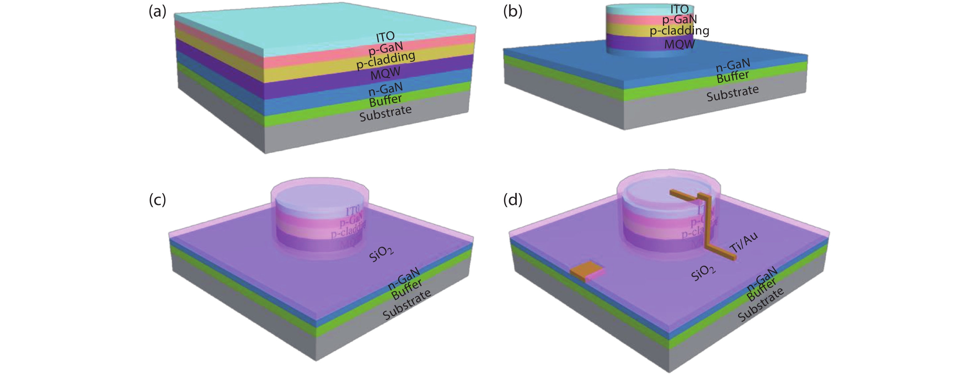
For micro-LED processing, the metal-organic chemical vapor deposition (MOCVD) is used to perform the epitaxial layer growth on the substrate. For example, the epitaxial GaN wafers grown on silicon substrate are introduced, and then chip fabrication process is carried out. The reason of making use of silicon as substrate here is that it has the advantages of large size, low cost, high thermal conductivity and can be integrated with Si based microelectronic devices. Also the silicon substrate has more advantages in the growth of high-efficiency LED with long emission wavelength, such as red, green and yellow[22]. A cleaned silicon is served as a substrate in MOCVD and the corresponding precursor gas is injected to grow the epitaxial LED layers. As shown in Fig. 1(a), it can be seen that the epitaxial layers mainly include a GaN buffer layer, an n-doped GaN layer, an InGaN/GaN multiple quantum well (MQW) layer, a current block layer of AlGaN, and a p-doped GaN layer. Then, a current spreading layer of indium tin oxide (ITO) was evaporated on top of the wafer. Then, the chip fabrication will be adopted to process the epi wafer, as shown in Fig. 1(b). ITO current spreading layer and epitaxial layer are patterned and etched to n-GaN layer by self-alignment, forming micro-LED mesa array. Then the SiO2 is deposited through plasma enhanced chemical vapor deposition (PECVD) as passivation layer and at last Ti/Au is deposited to serve as electrodes as shown in Figs. 1(c)1(d).

Figure  1.  (Color online) (a) The GaN-based epitaxial structure with silicon substrate. (b) Etching to n-GaN layer to form a micro-LED mesa array. (c) The deposition of SiO2 through PECVD. (d) The deposition of Ti/Au to serve as electrodes.

Herein, many performance tests have been carried out to verify the excellent characteristics of micro-LED. The I–V characteristics of micro-LED are similar to those of p–n junction diode in classical semiconductor theory. From the I–V curves of blue micro-LED pixels with different diameters prepared on the same epitaxial wafer, series resistance of the pixels increase with the decrease of chip size, as shown in Fig. 2(a)[23, 24]. The variation is mainly caused by the reduction of micro-LED size. Fig. 2(b) shows the curve of current density of blue micro-LED versus the bias voltage. The current crowding effect of small pixel is smaller and the current distribution is more uniform under the same bias voltage, so the current density of small pixel at the same voltage is higher.

Figure  2.  (Color online) (a) I–V curves of blue micro-LED pixels with different sizes. (b) The curve of current density for blue micro-LED with different sizes.

Optical properties are one of the fundamental and important properties of micro-LEDs, so other tests such as L–I also have been carried out. As shown in Fig. 3(a), it can be seen from the curve that the maximum output power increases with the increase of pixel size at the same current. And the curve of the corresponding light-output power versus current density is shown in Fig. 3(b). The smaller size of micro-LED devices, the higher maximum optical power density that can be output, and the smaller micro-LED devices can sustain higher injection current density according to the Fig. 2. The results also indicate that micro-LED has the advantages of high saturation current density and high light-output power density. Based on these performance tests, the brightness of micro-LED display can be up to 100 000 cd/m2[1]. Therefore the high luminance of micro-LED can easily satisfy the requirements for AR and other high-performance display applications.

Figure  3.  (Color online) (a) L–I curves of blue micro-LEDs with different diameters. (b) The curve of the light-output power density versus injection current density for blue micro-LED with different sizes.

After the corresponding electrical and optical properties were tested, the external quantum efficiency (EQE) and bandwidth were also analyzed[25, 26]. And the results indicated that the operating temperature of micro-LED can reach 500 K. Fig. 4(a) also shows the characteristic curve between EQE and current density on a semi-logarithmic scale with the device temperature varying from 300 to 500 K in 25 K increments. It can be seen that with the increase of temperature under the same current density, the EQE peak decreases a lot and the peak of EQE shifts to the high current density. At low current density, less than 10 A/cm2, the EQEs drop obviously with increasing temperature. The curve of bandwidth versus current density at different temperature is shown in Fig. 4(b), and it can be seen that the bandwidth shows different trend at different current densities. As the temperature increases from 300 to 425 K, the bandwidth decreases when the current density is below 2000 A/cm2. With the current density above 2500 A/cm2, the bandwidth increases with the increasing temperature.

Figure  4.  (Color online) (a) EQE versus current density from 300 to 500 K with 25 K temperature increment on a semi-logarithmic scale. (b) Bandwidth versus current from 300 to 425 K to show the trend with temperature[25]. Copyright 2014, Applied Physics Letters.

The driving modes of micro-LED are divided into passive matrix and active matrix[27, 28]. As shown in Fig. 5(a), during the dry etching of GaN down to the sapphire substrate and standard photo-lithography, the individual pixels are defined and a group of horizontal and vertical pixels share the same electrode to form a matrix structure respectively. Fig. 5(b) shows an active matrix structure, and we can see that the cathode of the pixel is connected through sharing n-GaN layer. In addition, the anode of all pixels is bonded with the Si-based CMOS driving backplate to form an individually addressable micro-LED array.

Figure  5.  (Color online) (a) The schematic of passive matrix micro-LED array[16]. (b) The schematic of active matrix micro-LED array[28]. Copyright 2015, IEEE Transactions on Electron Devices.

Also for the full-color display scheme, because of the continuous research of colorization and high brightness, many full-color display techniques have been developed, including RGB tricolor LED method by transfer printing red, green and blue micro-LEDs, UV or blue LED exciting color converters, and RGB micro-LED pixel through local strain engineering.

As shown in Fig. 6, the transfer printing scheme will be introduced. Capillary bonding is achieved by introducing an intermediate step to the transfer printing process, in which the substrate of the micro-LED being transferred is underetched by KOH solution[19]. After pick-up from the donor wafer, the backside is wetted on an acetone impregnated standard cleanroom wipe as shown in Figs. 6(a)6(b). Quick retraction of the stamp removes the micro-LED die from the wipe with its backside still wet, and it is then deposited onto the receiver substrate. After thermal curing, the micro-LED is bonded to the new substrate as shown in Figs. 6(c)6(d).

Figure  6.  (Color online) Schematic of transfer printing using capillary bonding. (a) Using an elastomeric stamp for the pick-up of a suspended micro-LED. (b) Upon pick-up, micro-LED is compressed against an acetone-wetted cloth. (c) Released micro-LED when the backside contacts receiving substrate. (d) After thermal curing, the micro-LED is bonded to the new substrate[19]. Copyright 2015, Optics Express.

At present, the massive transfer of micro-LED is still a bottleneck. The main technical challenges include the requirement of very high stability and accuracy of the transfer process. For RGB full-color display, as only single-color high-efficiency micro-LED can be developed on the same substrate, it is necessary to transfer the RGB micro-LEDs separately from different substrates, which requires very accurate technology to transfer a large amount of micro-LEDs that results in increasing difficulty of the transfer process.

Due to the high efficiency characteristics, the RGB technique may be the mainstream technique in the future[29, 30]. However, due to the different power efficiency and driving voltage of micro-LEDs with different colors, chromatic aberration may occur. Other full-color display schemes have been proposed for research which may alleviate such problems.

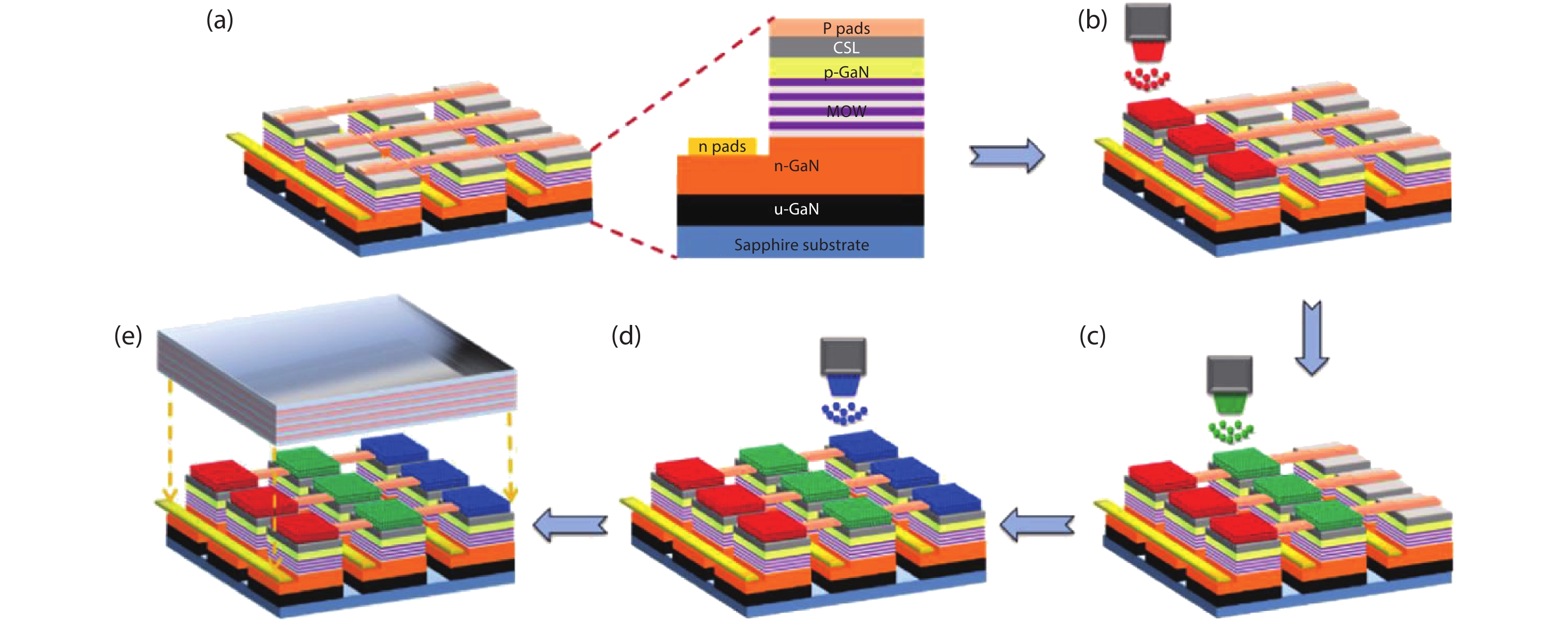
Here color conversion technique has also been researched, which mainly uses UV micro-LED to stimulate red, green and blue luminescent medium such as phosphor or QDs to produce light of specific wavelength, and then full-color display can be achieved through matching the tricolor[31, 32]. Due to the progress of QD technology, the particle size of QD is generally 1–10 nm, which can be applied to the micro-LED with smaller size, and the luminescence color is determined by the material and would be affected by the particle size. However, QD technology still has some drawbacks, such as poor stability, short life and packaging. At present, the technology of spin-coating and mist spraying has been used to develop hybrid micro-LED/QD device. The atomizer and airflow spray out uniform QDs with controllable size, to coat QDs on UV/blue LED to achieve full color display[19]. As shown in Fig. 7(a), standard MQW LED epitaxial layers are grown on sapphire substrates and etched to form UV micro-LED arrays. In Figs. 7(b)7(d), the aerosol jet printing method is used to spray the RGB QDs on the micro LED array. The QDs solution is aerosolized and entrained in a gas stream in this way. Therefore, the operation of spray is precisely controlled by the computer system, and the quantity of the QDs can be monitored in real time. In addition, Kuo et al. have performed another research to reduce the optical cross-talk effect through a simple lithography method. Photoresist is used to fabricate the mold, which consists of a window for QDs jetting and a blocking wall for optical cross-talk reduction[33]. Finally, in Fig. 7(e), a distributed Bragg reflector (DBR) is added to the top of micro LED arrays to reduce the leakage of UV light in the display application. There are still several disadvantages, for example, the phosphors or QDs may have low conversion efficiency as they are coated on the surface of micro-LED pixel.

Figure  7.  (Color online) (a) Standard MQW LED was grown on sapphire substrates for the micro-LED arrays. (b) The using of aerosol jet printing method to spray the red QDs on the micro-LED array. (c) The spraying of green QDs on the micro-LED array. (d) The spraying of blue QDs on the micro-LED array. (e) The DBR was added to the top of micro LED arrays[20]. Copyright 2015, Optic Express.

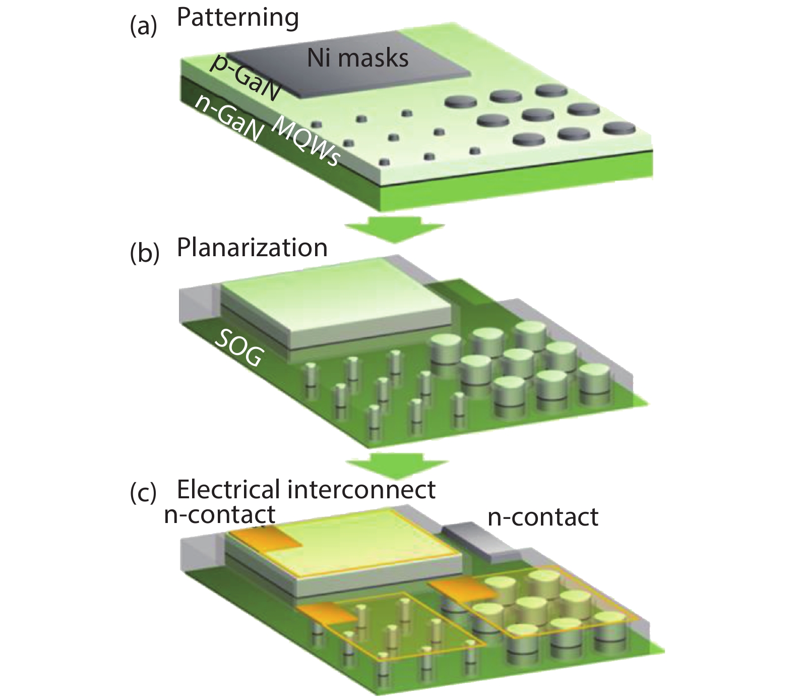
Growth methods, such as strain engineering method after the growth of epitaxial layer and chip fabrication, also have been designed to achieve full color on the same wafer[21]. The RGB subpixels are fabricated as schematically shown in Fig. 8. The blue and green colors are generated by local relaxation of the strain in the MQWs through using nanopillar structures, while the red color is generated by the membrane structure itself. Here the color is controllable by varying the nanopillar diameter of the MQWs. In this study, 150-nm diameter and 50-nm diameter nanopillars for the green emission and blue emission have been fabricated, respectively. And the fabrication process of the full-color LED pixel consisted of three major steps, including the fabrication of nanopillar structures by photolithography and etching, planarization and electrical insulation treatment, and finally the patterning of electrical interconnects, as shown in Figs. 8(a)8(c). Also, there still exist several problems need to be solved, such as the optimization of epitaxial growth of a longer (λ ~ 650 nm) wavelength micro-LED structure, the fabrication processes to yield better electrical properties for small-diameter nanopillar micro-LED, and an improvement of the subpixel areas and so on.

Figure  8.  (Color online) Schematic of the fabrication process for the RGB LED pixel. (a) The fabrication of nanopillar structures by photolithography and etching. (b) Planarization and electrical insulation treatment. (c) Formation of electrical interconnect[21]. Copyright 2017, Applied Physics Letters.

There are also many other full-color display schemes, such as optical lens synthesis. The RGB micro-LED arrays were packaged on three packaging boards respectively and connected with a control board and a trichromatic prism, and then the brightness of the trichromatic micro-LED is adjusted to achieve colorization[34]. At present, it is most likely to achieve a large-scale full-color display, mainly based on transfer printing and UV/blue micro-LED color conversion. Several related displays have been demonstrated[35, 36]. Although there still exist some technical problems to be solved, with the continuous research, these obstacles will be solved in the near future.

This review paper has described the basic characteristics and techniques of micro-LED for next-generation full-color display, mainly including the preparation process, the characteristics compared with LCD and OLED display, the related electrical performance and optical performance, and the full color techniques. With the development of micro-LED, it is expected that micro-LED will play an important role in academia and industry in the future display.

This work was supported by National Natural Science Foundation of China (NSFC) (61974031, 61705041 and 61571135); Shanghai Sailing Program (17YF1429100); Shanghai Technical Standard Program (18DZ2206000); State Key Laboratory of Intense Pulsed Radiation Simulation and Effect Funding (SKLIPR1607); National Key Research and Development Program of China (2017YFB0403603).


[1]
Lee H E, Shin J H, Park J H, et al. Micro light-emitting diodes for display and flexible biomedical applications. Adv Funct Mater, 2019, 29, 1808075 doi: 10.1002/adfm.201808075
[2]
Lee H E, Choi J, Lee S H, et al. Monolithic flexible vertical GaN light-emitting diodes for a transparent wireless brain optical stimulator. Adv Mater, 2018, 30, 1800649 doi: 10.1002/adma.201800649
[3]
Yang P, Zhang L, Kang D J, et al. High-resolution inkjet printing of quantum dot light-emitting microdiode arrays. Adv Opt Mater, 2019, 8, 1901429 doi: 10.1002/adom.201901429
[4]
Yang W, Zhang S, McKendry J J D, et al. Size-dependent capacitance study on InGaN-based micro-light-emitting diodes. J Appl Phys, 2014, 116, 044512 doi: 10.1063/1.4891233
[5]
Tian P, McKendry J J D, Gong Z, et al. Characteristics and applications of micro-pixelated GaN-based light emitting diodes on Si substrates. J Appl Phys, 2014, 115, 033112 doi: 10.1063/1.4862298
[6]
Li Y, Wu Q, Meng F Y, et al. Enhanced performance of large-area vertical light-emitting diodes treated by laser irradiation. Micro Nano Lett, 2017, 12, 369 doi: 10.1049/mnl.2016.0699
[7]
Chen X, Kong F, Li K, et al. Study of light extraction efficiency of flip-chip GaN-based LEDs with different periodic arrays. Opt Commun, 2014, 314, 90 doi: 10.1016/j.optcom.2013.09.006
[8]
Yao Y C, Hwang J M, Yang Z P, et al. Enhanced external quantum efficiency in GaN-based vertical-type light-emitting diodes by localized surface plasmons. Sci Rep, 2016, 6, 22659 doi: 10.1038/srep22659
[9]
Liu Z, Chong W C, Wong K M, et al. GaN-based LED micro-displays for wearable applications. Microelectron Eng, 2015, 148, 98 doi: 10.1016/j.mee.2015.09.007
[10]
Lin C C, Fang Y H, Kao M J, et al. Ultra-fine pitch thin-film micro LED display for indoor applications. SID Symp Dig Tech Pap, 2018, 49, 782 doi: 10.1002/sdtp.12373
[11]
Yoon J K, Park E M, Son J S, et al. The study of picture quality of OLED TV with WRGB OLEDs structure. SID Symp Dig Tech Pap, 2013, 44, 326 doi: 10.1002/j.2168-0159.2013.tb06212.x
[12]
Katsui S, Kobayashi H, Nakagawa T, et al. 5291-PPI organic light-emitting diode display using field-effect transistors including a c-axis aligned crystalline oxide semiconductor. SID Symp Dig Tech Pap, 2019, 50, 311 doi: 10.1002/sdtp.12918
[13]
Liu Z, Zhang K, Liu Y, et al. Fully multi-functional GaN-based micro-LEDs for 2500 PPI micro-displays, temperature sensing, light energy harvesting, and light detection. 64th IEEE Annual International Electron Devices Meeting, 2018, 871
[14]
JBD exhibits 2000000 nit and 10000 PPI micro-LED displays [EB/OL]. https://www.toutiao.com/i6705923322162446856/
[15]
Santos J M M, Jones B E, Schlosser P J, et al. Hybrid GaN LED with capillary-bonded II–VI MQW color-converting membrane for visible light communications. Semicond Sci Tech, 2015, 30, 035012 doi: 10.1088/0268-1242/30/3/035012
[16]
Hori A, Yasunaga D, Satake A, et al. Temperature and injection current dependence of electroluminescence intensity in green and blue InGaN single-quantum-well light-emitting diodes. J Appl Phys, 2003, 93, 3152 doi: 10.1063/1.1554475
[17]
Chong W C, Cho W K, Liu Z J, et al. 1700 pixels per inch (PPI) passive-matrix micro-LED display powered by ASIC. 2014 IEEE Compound Semiconductor Integrated Circuit Symposium (CSICS), 2014, 978-1-4799-3622-9
[18]
Fei M Q, Fei Y. The wide view-angle technique of TFT-LCD. Adv Display, 2008, 11, 22
[19]
Trindade A J, Guilhabert B, Xie E Y, et al. Heterogeneous integration of gallium nitride light-emitting diodes on diamond and silica by transfer printing. Opt Express, 2015, 23, 9329 doi: 10.1364/OE.23.009329
[20]
Han H V, Lin H Y, Lin C C, et al. Resonant-enhanced full-color emission of quantum-dot-based micro LED display technology. Opt Express, 2015, 23, 32504 doi: 10.1364/OE.23.032504
[21]
Chung K, Sui J, Demory B, et al. Color mixing from monolithically integrated InGaN-based light-emitting diodes by local strain engineering. Appl Phys Lett, 2017, 111, 041101 doi: 10.1063/1.4995561
[22]
Jiang F, Zhang J, Xu L, et al. Efficient InGaN-based yellow-light-emitting diodes. Photonics Res, 2019, 7, 144 doi: 10.1364/PRJ.7.000144
[23]
Tian P, McKendry J J, Gu E, et al. Fabrication, characterization and applications of flexible vertical InGaN micro-light emitting diode arrays. Opt Express, 2016, 24, 699 doi: 10.1364/OE.24.000699
[24]
Tian P, Althumali A, Gu E, et al. Aging characteristics of blue InGaN micro-light emitting diodes at an extremely high current density of 3.5 kA cm−2. Semicond Sci Tech, 2016, 31, 045005 doi: 10.1088/0268-1242/31/4/045005
[25]
Tian P, McKendry J J D, Herrnsdorf J, et al. Temperature-dependent efficiency droop of blue InGaN micro-light emitting diodes. Appl Phys Lett, 2014, 105, 171107 doi: 10.1063/1.4900865
[26]
Gong Z, Jin S, Chen Y, et al. Size-dependent light output, spectral shift, and self-heating of 400 nm InGaN light-emitting diodes. J Appl Phys, 2010, 107, 013103 doi: 10.1063/1.3276156
[27]
Zhang K, Peng D, Lau K M, et al. Fully-integrated active matrix programmable UV and blue micro-LED display system-on-panel (SoP). J Soc Inf Display, 2017, 25, 240 doi: 10.1002/jsid.550
[28]
Herrnsdorf J, McKendry J J D, Zhang S, et al. Active-matrix GaN micro light-emitting diode display with unprecedented brightness. IEEE T Electron Dev, 2015, 62, 1918 doi: 10.1109/TED.2015.2416915
[29]
Tull B R, Twu N, Hsu Y J, et al. Micro-LED microdisplays by integration of III–V LEDs with silicon thin film transistors. SID Symp Dig Tech Pap, 2017, 48, 246 doi: 10.1002/sdtp.11680
[30]
Cao J, Liu X, Khan M A, et al. RGB tricolor produced by white-based top-emitting organic light-emitting diodes with microcavity structure. Curr Appl Phys, 2007, 7, 300 doi: 10.1016/j.cap.2006.09.002
[31]
Sato Y, Takahashi N, Sato S. Full-color fluorescent display devices using a near-UV light-emitting diode. Jpn J Appl Phys, 1996, 35, L838 doi: 10.1143/JJAP.35.L838
[32]
Kim B H, Nam S, Oh N, et al. Multilayer transfer printing for pixelated, multi-color quantum dot light-emitting diodes. ACS Nano, 2016, 10, 4920 doi: 10.1021/acsnano.5b06387
[33]
Lin H Y, Sher C W, Hsieh D H, et al. Optical cross-talk reduction in a quantum-dot-based full-color micro-light-emitting-diode display by a lithographic-fabricated photoresist mold. Photonics Res, 2017, 5, 411 doi: 10.1364/PRJ.5.000411
[34]
Liu Z, Chong W C, Wong K M, et al. A novel BLU-free full-color LED projector using LED on silicon micro-displays. IEEE Photonic Tech Lett, 2013, 25, 2267 doi: 10.1109/LPT.2013.2285229
[35]
Display technology of micro-LED has the most potential application in AR/VR display device [EB/OL]. http://www.51touch.com/lcd/news/dynamic/2017/1031/48607.html
[36]
Color conversion is a feasible way for micro LED display technology to achieve mass production [EB/OL]. http://www.yejibang.com/news-details-23615.html
Fig. 1.  (Color online) (a) The GaN-based epitaxial structure with silicon substrate. (b) Etching to n-GaN layer to form a micro-LED mesa array. (c) The deposition of SiO2 through PECVD. (d) The deposition of Ti/Au to serve as electrodes.

Fig. 2.  (Color online) (a) I–V curves of blue micro-LED pixels with different sizes. (b) The curve of current density for blue micro-LED with different sizes.

Fig. 3.  (Color online) (a) L–I curves of blue micro-LEDs with different diameters. (b) The curve of the light-output power density versus injection current density for blue micro-LED with different sizes.

Fig. 4.  (Color online) (a) EQE versus current density from 300 to 500 K with 25 K temperature increment on a semi-logarithmic scale. (b) Bandwidth versus current from 300 to 425 K to show the trend with temperature[25]. Copyright 2014, Applied Physics Letters.

Fig. 5.  (Color online) (a) The schematic of passive matrix micro-LED array[16]. (b) The schematic of active matrix micro-LED array[28]. Copyright 2015, IEEE Transactions on Electron Devices.

Fig. 6.  (Color online) Schematic of transfer printing using capillary bonding. (a) Using an elastomeric stamp for the pick-up of a suspended micro-LED. (b) Upon pick-up, micro-LED is compressed against an acetone-wetted cloth. (c) Released micro-LED when the backside contacts receiving substrate. (d) After thermal curing, the micro-LED is bonded to the new substrate[19]. Copyright 2015, Optics Express.

Fig. 7.  (Color online) (a) Standard MQW LED was grown on sapphire substrates for the micro-LED arrays. (b) The using of aerosol jet printing method to spray the red QDs on the micro-LED array. (c) The spraying of green QDs on the micro-LED array. (d) The spraying of blue QDs on the micro-LED array. (e) The DBR was added to the top of micro LED arrays[20]. Copyright 2015, Optic Express.

Fig. 8.  (Color online) Schematic of the fabrication process for the RGB LED pixel. (a) The fabrication of nanopillar structures by photolithography and etching. (b) Planarization and electrical insulation treatment. (c) Formation of electrical interconnect[21]. Copyright 2017, Applied Physics Letters.

Table 1.   The comparison of main characteristics of micro-LED, LCD, and OLED.

ParameterLCDOLEDmicro-LED
Emission typeBacklight/LED (thick)Self-emissive (thin)Self-emissive (thin)
Brightness (cd/m2)30005000100 000[1]
Luminescent materialInorganicOrganicInorganic
Contrast ratio5000 : 1[1]
PPI> 3001500–6000[12]1500–10 000[14, 17]
Color gamut75%, NTSC> 100%, NTSC> 100%, NTSC[1]
Viewing angleBest (~178°)[18]Best (~178°)Best (~178°)[1]
Response time5 ms, slow10 μs, medium0.2 ns, fast[1]
LifetimeMediumMediumLong[1]
Operating temperature233–373 K238–358 K15–500 K[1, 12, 15]
DownLoad: CSV
[1]
Lee H E, Shin J H, Park J H, et al. Micro light-emitting diodes for display and flexible biomedical applications. Adv Funct Mater, 2019, 29, 1808075 doi: 10.1002/adfm.201808075
[2]
Lee H E, Choi J, Lee S H, et al. Monolithic flexible vertical GaN light-emitting diodes for a transparent wireless brain optical stimulator. Adv Mater, 2018, 30, 1800649 doi: 10.1002/adma.201800649
[3]
Yang P, Zhang L, Kang D J, et al. High-resolution inkjet printing of quantum dot light-emitting microdiode arrays. Adv Opt Mater, 2019, 8, 1901429 doi: 10.1002/adom.201901429
[4]
Yang W, Zhang S, McKendry J J D, et al. Size-dependent capacitance study on InGaN-based micro-light-emitting diodes. J Appl Phys, 2014, 116, 044512 doi: 10.1063/1.4891233
[5]
Tian P, McKendry J J D, Gong Z, et al. Characteristics and applications of micro-pixelated GaN-based light emitting diodes on Si substrates. J Appl Phys, 2014, 115, 033112 doi: 10.1063/1.4862298
[6]
Li Y, Wu Q, Meng F Y, et al. Enhanced performance of large-area vertical light-emitting diodes treated by laser irradiation. Micro Nano Lett, 2017, 12, 369 doi: 10.1049/mnl.2016.0699
[7]
Chen X, Kong F, Li K, et al. Study of light extraction efficiency of flip-chip GaN-based LEDs with different periodic arrays. Opt Commun, 2014, 314, 90 doi: 10.1016/j.optcom.2013.09.006
[8]
Yao Y C, Hwang J M, Yang Z P, et al. Enhanced external quantum efficiency in GaN-based vertical-type light-emitting diodes by localized surface plasmons. Sci Rep, 2016, 6, 22659 doi: 10.1038/srep22659
[9]
Liu Z, Chong W C, Wong K M, et al. GaN-based LED micro-displays for wearable applications. Microelectron Eng, 2015, 148, 98 doi: 10.1016/j.mee.2015.09.007
[10]
Lin C C, Fang Y H, Kao M J, et al. Ultra-fine pitch thin-film micro LED display for indoor applications. SID Symp Dig Tech Pap, 2018, 49, 782 doi: 10.1002/sdtp.12373
[11]
Yoon J K, Park E M, Son J S, et al. The study of picture quality of OLED TV with WRGB OLEDs structure. SID Symp Dig Tech Pap, 2013, 44, 326 doi: 10.1002/j.2168-0159.2013.tb06212.x
[12]
Katsui S, Kobayashi H, Nakagawa T, et al. 5291-PPI organic light-emitting diode display using field-effect transistors including a c-axis aligned crystalline oxide semiconductor. SID Symp Dig Tech Pap, 2019, 50, 311 doi: 10.1002/sdtp.12918
[13]
Liu Z, Zhang K, Liu Y, et al. Fully multi-functional GaN-based micro-LEDs for 2500 PPI micro-displays, temperature sensing, light energy harvesting, and light detection. 64th IEEE Annual International Electron Devices Meeting, 2018, 871
[14]
JBD exhibits 2000000 nit and 10000 PPI micro-LED displays [EB/OL]. https://www.toutiao.com/i6705923322162446856/
[15]
Santos J M M, Jones B E, Schlosser P J, et al. Hybrid GaN LED with capillary-bonded II–VI MQW color-converting membrane for visible light communications. Semicond Sci Tech, 2015, 30, 035012 doi: 10.1088/0268-1242/30/3/035012
[16]
Hori A, Yasunaga D, Satake A, et al. Temperature and injection current dependence of electroluminescence intensity in green and blue InGaN single-quantum-well light-emitting diodes. J Appl Phys, 2003, 93, 3152 doi: 10.1063/1.1554475
[17]
Chong W C, Cho W K, Liu Z J, et al. 1700 pixels per inch (PPI) passive-matrix micro-LED display powered by ASIC. 2014 IEEE Compound Semiconductor Integrated Circuit Symposium (CSICS), 2014, 978-1-4799-3622-9
[18]
Fei M Q, Fei Y. The wide view-angle technique of TFT-LCD. Adv Display, 2008, 11, 22
[19]
Trindade A J, Guilhabert B, Xie E Y, et al. Heterogeneous integration of gallium nitride light-emitting diodes on diamond and silica by transfer printing. Opt Express, 2015, 23, 9329 doi: 10.1364/OE.23.009329
[20]
Han H V, Lin H Y, Lin C C, et al. Resonant-enhanced full-color emission of quantum-dot-based micro LED display technology. Opt Express, 2015, 23, 32504 doi: 10.1364/OE.23.032504
[21]
Chung K, Sui J, Demory B, et al. Color mixing from monolithically integrated InGaN-based light-emitting diodes by local strain engineering. Appl Phys Lett, 2017, 111, 041101 doi: 10.1063/1.4995561
[22]
Jiang F, Zhang J, Xu L, et al. Efficient InGaN-based yellow-light-emitting diodes. Photonics Res, 2019, 7, 144 doi: 10.1364/PRJ.7.000144
[23]
Tian P, McKendry J J, Gu E, et al. Fabrication, characterization and applications of flexible vertical InGaN micro-light emitting diode arrays. Opt Express, 2016, 24, 699 doi: 10.1364/OE.24.000699
[24]
Tian P, Althumali A, Gu E, et al. Aging characteristics of blue InGaN micro-light emitting diodes at an extremely high current density of 3.5 kA cm−2. Semicond Sci Tech, 2016, 31, 045005 doi: 10.1088/0268-1242/31/4/045005
[25]
Tian P, McKendry J J D, Herrnsdorf J, et al. Temperature-dependent efficiency droop of blue InGaN micro-light emitting diodes. Appl Phys Lett, 2014, 105, 171107 doi: 10.1063/1.4900865
[26]
Gong Z, Jin S, Chen Y, et al. Size-dependent light output, spectral shift, and self-heating of 400 nm InGaN light-emitting diodes. J Appl Phys, 2010, 107, 013103 doi: 10.1063/1.3276156
[27]
Zhang K, Peng D, Lau K M, et al. Fully-integrated active matrix programmable UV and blue micro-LED display system-on-panel (SoP). J Soc Inf Display, 2017, 25, 240 doi: 10.1002/jsid.550
[28]
Herrnsdorf J, McKendry J J D, Zhang S, et al. Active-matrix GaN micro light-emitting diode display with unprecedented brightness. IEEE T Electron Dev, 2015, 62, 1918 doi: 10.1109/TED.2015.2416915
[29]
Tull B R, Twu N, Hsu Y J, et al. Micro-LED microdisplays by integration of III–V LEDs with silicon thin film transistors. SID Symp Dig Tech Pap, 2017, 48, 246 doi: 10.1002/sdtp.11680
[30]
Cao J, Liu X, Khan M A, et al. RGB tricolor produced by white-based top-emitting organic light-emitting diodes with microcavity structure. Curr Appl Phys, 2007, 7, 300 doi: 10.1016/j.cap.2006.09.002
[31]
Sato Y, Takahashi N, Sato S. Full-color fluorescent display devices using a near-UV light-emitting diode. Jpn J Appl Phys, 1996, 35, L838 doi: 10.1143/JJAP.35.L838
[32]
Kim B H, Nam S, Oh N, et al. Multilayer transfer printing for pixelated, multi-color quantum dot light-emitting diodes. ACS Nano, 2016, 10, 4920 doi: 10.1021/acsnano.5b06387
[33]
Lin H Y, Sher C W, Hsieh D H, et al. Optical cross-talk reduction in a quantum-dot-based full-color micro-light-emitting-diode display by a lithographic-fabricated photoresist mold. Photonics Res, 2017, 5, 411 doi: 10.1364/PRJ.5.000411
[34]
Liu Z, Chong W C, Wong K M, et al. A novel BLU-free full-color LED projector using LED on silicon micro-displays. IEEE Photonic Tech Lett, 2013, 25, 2267 doi: 10.1109/LPT.2013.2285229
[35]
Display technology of micro-LED has the most potential application in AR/VR display device [EB/OL]. http://www.51touch.com/lcd/news/dynamic/2017/1031/48607.html
[36]
Color conversion is a feasible way for micro LED display technology to achieve mass production [EB/OL]. http://www.yejibang.com/news-details-23615.html
1

A High Performance AlGaN/GaN HEMT with a New Method for T-Gate Layout Design

Chen Zhigang, Zhang Yang, Luo Weijun, Zhang Renping, Yang Fuhua, et al.

Journal of Semiconductors, 2008, 29(9): 1654-1656.

2

Effect of a Metal Buffer Layer on GaN Grown on Si(111) by Gas Source Molecular Beam Epitaxy with Ammonia

Lin Guoqiang, Zeng Yiping, Wang Xiaoliang, Liu Hongxin

Journal of Semiconductors, 2008, 29(10): 1998-2002.

3

Influences of N2 Flow Rate on the Crystalline Characteristics of GaN Films Deposited on Glass Substrate at Low Temperature

Wang Wenyan, Qin Fuwen, Wu Aimin, Song Shiwei, Liu Ruixian, et al.

Journal of Semiconductors, 2008, 29(12): 2376-2380.

4

Effects of in situ Annealing on Optical and Structural Properties of GaN Epilayers Grown by HVPE

Duan Chenghong, Qiu Kai, Li Xinhua, Zhong Fei, Yin Zhijun, et al.

Journal of Semiconductors, 2008, 29(3): 410-413.

5

Influence of Threading Dislocations on the Luminescence Efficiency of GaN Heteroepitaxial Layers

Gao Zhiyuan, Hao Yue, Li Peixian, Zhang Jincheng

Journal of Semiconductors, 2008, 29(3): 521-525.

6

Analyses in Reliability of GaN-Based High Power Light Emitting Diodes

Chen Yu, Wang Liangchen, Yi Xiaoyan, Wang Libin, Liu Zhiqiang, et al.

Chinese Journal of Semiconductors , 2007, 28(S1): 500-503.

7

Growth of GaN on Si(1 l 1) by Inserting 5AI/AIN Buffer Layer

Guo Lunchun, Wang Xiaoliang, Hu Guoxin, Li Jianping, Luo Weijun, et al.

Chinese Journal of Semiconductors , 2007, 28(S1): 234-237.

8

Numerical Simulation of Gas Phase and Surface Reaction for Growth of GaN by MOCVD

Gao Lihua, Yang Yunke, Chen Haixin, Fu Song

Chinese Journal of Semiconductors , 2007, 28(S1): 245-248.

9

Observation of Dislocation Etch Pits in GaN Epilayers by Atomic Force Microscopy and Scanning Electron Microscopy

Gao Zhiyuan, Hao Yue, Zhang Jincheng, Zhang Jinfeng, Chen Haifeng, et al.

Chinese Journal of Semiconductors , 2007, 28(4): 473-479.

10

Growth of Thick GaN Films on Mixed-Polarity Buffer by Halide Vapor Phase Epitaxy

Yin Zhijun, Zhong Fei, Qiu Kai, Li Xinhua, Wang Yuqi, et al.

Chinese Journal of Semiconductors , 2007, 28(6): 909-912.

11

Theoretical Simulation of Vertical HVPE Reactor and GaN Thick Film Growth

Ma Ping, Duan Yao, Wei Tongbo, Duan Ruifei, Wang Junxi, et al.

Chinese Journal of Semiconductors , 2007, 28(S1): 253-256.

12

Microstructure of an InGaN/GaN Multiple Quantum Well LED on Si (111) Substrate

Li Cuiyun, Zhu Hua, Mo Chunlan, Jiang Fengyi

Chinese Journal of Semiconductors , 2006, 27(11): 1950-1954.

13

GaAs/GaN Direct Wafer Bonding Based on Hydrophilic Surface Treatment

Wang Hui, Guo Xia, Liang Ting, Liu Shiwen, Gao Guo, et al.

Chinese Journal of Semiconductors , 2006, 27(6): 1042-1045.

14

Light-Assisted Wet Etching of Dislocations in GaN Grown on Silicon

Zhao Liwei, Liu Caichi, Teng Xiaoyun, Hao Qiuyan, Zhu Junshan, et al.

Chinese Journal of Semiconductors , 2006, 27(6): 1046-1050.

15

0.25μm Gate-Length AlGaN/GaN Power HEMTs on Sapphire with fT of 77GHz

Zheng Yingkui, Liu Guoguo, He Zhijing, Liu Xinyu, Wu Dexin, et al.

Chinese Journal of Semiconductors , 2006, 27(6): 963-965.

16

Characteristics of npn AlGaN/GaN HBT

Gong Xin, Ma Lin, Zhang Xiaoju, Zhang Jinfeng, Yang Yan, et al.

Chinese Journal of Semiconductors , 2006, 27(9): 1600-1603.

17

Dislocation Reduction in GaN on Sapphire by Epitaxial Lateral Overgrowth

Chen Jun, Wang Jianfeng, Wang Hui, Zhao Degang, Zhu Jianjun, et al.

Chinese Journal of Semiconductors , 2006, 27(3): 419-424.

18

Optimization of the Electron Blocking Layer in GaN Laser Diodes

Li Ti, Pan Huapu, Xu Ke, Hu Xiaodong

Chinese Journal of Semiconductors , 2006, 27(8): 1458-1462.

19

Epitaxial Lateral Overgrowth of High Quality GaN by MOCVD

Chen Jun, Zhang Jicai, Zhang Shuming, Zhu Jianjun, Yang Hui, et al.

Chinese Journal of Semiconductors , 2005, 26(S1): 106-108.

20

Investigation of Undoped AlGaN/GaN Microwave Power HEMT

Zeng Qingming, Li Xianjie, Zhou Zhou, Wang Yong, Wang Xiaoliang, et al.

Chinese Journal of Semiconductors , 2005, 26(S1): 151-154.

1. Yan, Q., Liang, T., Zhang, K. et al. Light Extraction and Shaping Technique for Micro-LED Displays (Invited) | [Micro-LED 显示光提取与光整形技术研究进展(特邀)]. Guangxue Xuebao/Acta Optica Sinica, 2025, 45(8): 0800001. doi:10.3788/AOS241921
2. Lai, Z., Zou, Z., Ye, J. et al. Fabrication of uniform submicron metal bump arrays based on undercut sacrificial layer for lift-off process. Journal of Materials Science: Materials in Electronics, 2025, 36(12): 692. doi:10.1007/s10854-025-14764-5
3. Huang, X., Lang, T., Tang, X. et al. Improved indium bumps bonding process using flexible composite structure temporary substrate for micro-LED display applications. Materials Science in Semiconductor Processing, 2025. doi:10.1016/j.mssp.2024.109018
4. Liu, Z., Ren, K., Liu, Y. et al. Improving Optical Efficiency and Luminance of GaN-Based Micro-Light-Emitting Diodes for High-Resolution Displays via NH3 Plasma Pretreatment. ACS Applied Materials and Interfaces, 2025, 17(1): 1420-1427. doi:10.1021/acsami.4c12317
5. Wang, S., Lu, Y., Zhang, K. et al. Electroless fabrication of super uniform nickel bumps on the TFT driver substrates for micro-LED display. Journal of the Society for Information Display, 2025. doi:10.1002/jsid.2088
6. Memon, M.H., Yu, H., Kang, Y. et al. A Gate-Assisted Dual-Functional GaN p-n Diode for High-Speed Visible Light Communication. IEEE Electron Device Letters, 2025. doi:10.1109/LED.2025.3565044
7. Huang, X., Liu, Q., Jiang, J. et al. High-Yield and High-Accuracy Mass Transfer of Full-Color Micro-LEDs Using a Blister-Type Dynamic Release Polymer. ACS Applied Materials and Interfaces, 2025. doi:10.1021/acsami.5c01531
8. Zhang, H., Wang, H., Du, J. et al. Linearly polarized GaN micro-LED with adjustable directional emission integrated with a continuous metasurface. Journal of Applied Physics, 2024, 136(2): 023106. doi:10.1063/5.0211495
9. Jiang, M., Zhang, L., Zhou, X. et al. Wafer level quasi-van der Waals epitaxy of AlGaN/GaN heterojunctions on sp2-bonded BN controlled by AlN nucleation layer. Applied Surface Science, 2024. doi:10.1016/j.apsusc.2024.159902
10. Lu, Y., Lin, C., Tian, L. et al. Electroless deposition of high-uniformity nickel microbumps with ultrahigh resolution of 8 μm pitch for monolithic Micro-LED display. Materials Science in Semiconductor Processing, 2024. doi:10.1016/j.mssp.2024.108263
11. Luo, C., Lin, C., Ye, J. et al. Electroplating of Cu/Sn bumps with ultrafine pitch and high uniformity for micro-LED interconnection. Journal of Materials Science: Materials in Electronics, 2024, 35(12): 878. doi:10.1007/s10854-024-12645-x
12. Li, S.-H., Sun, C., Tang, P.-Y. et al. Augmented reality system based on the integration of polarization-independent metalens and micro-LEDs. Optics Express, 2024, 32(7): 11463-11473. doi:10.1364/OE.517356
13. Lee, B., Ryu, H.-Y. Investigation into the Effects of Cross-Sectional Shape and Size on the Light-Extraction Efficiency of GaN-Based Blue Nanorod Light-Emitting Diode Structures. Crystals, 2024, 14(3): 241. doi:10.3390/cryst14030241
14. Zhang, J., Melanson, B., Seitz, M. et al. III-Nitride ultraviolet and visible LEDs. Comprehensive Semiconductor Science and Technology, Second Edition: Volumes 1-3, 2024. doi:10.1016/B978-0-323-96027-4.00039-5
15. Chen, Y.-R., Chang, S.-J., Hsueh, T.-J. A Co-Planarized Common Cathode Micro-LED Display That Is Produced Using Planarization and a Copper Process. IEEE Electron Device Letters, 2024, 45(10): 1875-1878. doi:10.1109/LED.2024.3442436
16. Javaid, A., Mahmood, N., Mehmood, M.Q. Miniaturized and high efficient GaN-based blue micro-LEDs for future display applications. Proceedings of SPIE - The International Society for Optical Engineering, 2024. doi:10.1117/12.3022180
17. Liu, Z., Ren, K., Liu, Y. et al. GaN-Based Micro-LED Sidewall Defect Reduction via Plasma Pre-Treatment and Atomic Layer Deposition. Digest of Technical Papers - SID International Symposium, 2024, 55(S1): 1312-1314. doi:10.1002/sdtp.17350
18. Lu, Y., Lin, C., Wang, S. et al. Electroless deposition of nickel microbumps for fine-pith flip-chip bonding. Journal of Physics: Conference Series, 2024, 2783(1): 012022. doi:10.1088/1742-6596/2783/1/012022
19. Mishra, R.K., Verma, K., Chianella, I. et al. Nanomaterial integration in micro LED technology: Enhancing efficiency and applications. Next Nanotechnology, 2024. doi:10.1016/j.nxnano.2024.100056
20. Pan, K., Zhang, K., Deng, L. et al. Monolithically and Vertically Integrated LED-on-FET Device Based on a Novel GaN Epitaxial Structure. IEEE Transactions on Electron Devices, 2023, 70(12): 6393-6398. doi:10.1109/TED.2023.3321705
21. González-Izquierdo, P., Rochat, N., Zoccarato, D. et al. Influence of Shape and Size on GaN/InGaN μLED Light Emission: A Competition between Sidewall Defects and Light Extraction Efficiency. ACS Photonics, 2023, 10(11): 4031-4037. doi:10.1021/acsphotonics.3c00971
22. Weng, Y., Chen, G., Zhou, X. et al. Design and fabrication of patterned high performance quantum-dot color conversion films for μLED full color display applications. Journal of Luminescence, 2023. doi:10.1016/j.jlumin.2023.119892
23. Huang, W.-T., Hong, L.-X., Liu, R.-S. Nanostructure Control of GaN by Electrochemical Etching for Enhanced Perovskite Quantum Dot LED Backlighting. ACS Applied Materials and Interfaces, 2023, 15(33): 39505-39512. doi:10.1021/acsami.3c06257
24. Melanson, B., Seitz, M., Zhang, J. Demonstration of Trench Isolated Monolithic GaN μLED Displays Enabled by Photoresist Planarization. IEEE Photonics Journal, 2023, 15(4): 8200708. doi:10.1109/JPHOT.2023.3298566
25. Xu, F., Wang, G., Tao, T. et al. Optimized InGaN/GaN Quantum Structure for High-Efficiency Micro-LEDs Displays With Low Current Injection. IEEE Transactions on Electron Devices, 2023, 70(8): 4257-4263. doi:10.1109/TED.2023.3283942
26. González-Izquierdo, P., Rochat, N., Charles, M. et al. Kelvin Probe Force Microscopy under Variable Illumination: A Novel Technique To Unveil Charge Carrier Dynamics in GaN. Journal of Physical Chemistry C, 2023, 127(26): 12727-12734. doi:10.1021/acs.jpcc.3c01887
27. Liu, Z., Ren, K., Dai, G. et al. A Review on Micro-LED Display Integrating Metasurface Structures. Micromachines, 2023, 14(7): 1354. doi:10.3390/mi14071354
28. Kaçar, R., Serin, R.B., Uçar, E. et al. A review of high-end display technologies focusing on inkjet printed manufacturing. Materials Today Communications, 2023. doi:10.1016/j.mtcomm.2023.105534
29. Nie, J., Zhang, Z., Chen, K. et al. Systematic study on size and temporal dependence of micro-LED arrays for display applications. Photonics Research, 2023, 11(4): 549-557. doi:10.1364/PRJ.479593
30. Hartensveld, M.. InGaN Color Tunable Full Color Passive Matrix. IEEE Electron Device Letters, 2023, 44(3): 460-463. doi:10.1109/LED.2023.3237512
31. Ma, T., Chen, J., Chen, Z. et al. Progress in Color Conversion Technology for Micro-LED. Advanced Materials Technologies, 2023, 8(1): 2200632. doi:10.1002/admt.202200632
32. Hartensveld, M.. Demonstration of Color Tunable μLED Passive Matrix. Digest of Technical Papers - SID International Symposium, 2023, 54(1): 1770-1773. doi:10.1002/sdtp.16947
33. Yan, Q., Nie, J., Huang, Z. et al. Temporal Study of Micro-LED Arrays for Potential High Efficiency Driving. Digest of Technical Papers - SID International Symposium, 2023, 54(1): 402-405. doi:10.1002/sdtp.16577
34. Xia, T., Liu, Y., Huang, Z. et al. Improving the front emission of Micro-LED by using a sidewall light guide structure. Digest of Technical Papers - SID International Symposium, 2023, 54(S1): 32-36. doi:10.1002/sdtp.16213
35. Ye, P., Gui, Y., Li, Y. et al. Simulation Investigation On The Characteristics Of Gan-Based Multi-Quantum Wells Micro-Leds. 2023. doi:10.1109/CSTIC58779.2023.10219272
36. Melanson, B., Seitz, M., Zhang, J. Photoresist Planarized Trench Isolation for Monolithic GaN µLED Displays. Proceedings of SPIE - The International Society for Optical Engineering, 2023. doi:10.1117/12.2649346
37. Zhang, Z.-Z., Yang, J., Zhao, D.-G. et al. Influence of the lattice parameter of the AlN buffer layer on the stress state of GaN film grown on (111) Si. Chinese Physics B, 2023, 32(2): 028101. doi:10.1088/1674-1056/ac6b2b
38. Ou, C.-J., Chang, K.-P., Tasi, M.-W. et al. Detailed Successive Layer Modeling and Design Factor Analysis for Single Micro-LED Pixel. IEEE Photonics Journal, 2022, 14(6): 7059309. doi:10.1109/JPHOT.2022.3218765
39. Hao, S., Ye, J., Guo, C. et al. Fully GaN Monolithic Integrated Light Emitting Triode-on-Bipolar Junction Transistor Device Drivable with Small Current Signals and Its Frequency Response Characteristic: A Modeling and Simulation Study. Physica Status Solidi (A) Applications and Materials Science, 2022, 219(24): 2200606. doi:10.1002/pssa.202200606
40. Kim, S., Lee, H., Jung, G.-H. et al. Self-array of one-dimensional GaN nanorods using the electric field on dielectrophoresis for the photonic emitters of display pixel. Nanoscale Advances, 2022, 5(4): 1079-1085. doi:10.1039/d2na00496h
41. Kumar, G., Agrawal, S. Suppression of Ambipolar Current in Enhanced Gate Based Schottky Barrier CNTFET Using Ant Lion Optimization. Silicon, 2022, 14(17): 11531-11537. doi:10.1007/s12633-022-01807-3
42. Lee, T.-Y., Chen, L.-Y., Lo, Y.-Y. et al. Technology and Applications of Micro-LEDs: Their Characteristics, Fabrication, Advancement, and Challenges. ACS Photonics, 2022, 9(9): 2905-2930. doi:10.1021/acsphotonics.2c00285
43. Chang, K.-P., Wu, C.-J., Lo, C.-W. et al. Synthesis of SiO2-coated CdSe/ZnS quantum dots using various dispersants in the photoresist for color-conversion micro-LED displays. Materials Science in Semiconductor Processing, 2022. doi:10.1016/j.mssp.2022.106790
44. Hu, X., Cai, J., Ye, Y. et al. Simulation Model of GaN-Based Micro-LED with High Light Extraction Efficiency | [高光效GaN基Micro-LED仿真模型研究]. Guangxue Xuebao/Acta Optica Sinica, 2022, 42(15): 1525001. doi:10.3788/AOS202242.1525001
45. Zhao, Z.-H., Xue, F.-N., Zhao, P.-B. et al. Theoretical study of potential n-type and p-type dopants in GaN from data mining and first-principles calculation. Semiconductor Science and Technology, 2022, 37(8): 085004. doi:10.1088/1361-6641/ac7740
46. Liu, X., Yuan, Z., Zhou, G. et al. Improving the efficiency of micro-LEDs at high current densities employing a micro-current spreading layer-confined structure. Applied Physics B: Lasers and Optics, 2022, 128(7): 121. doi:10.1007/s00340-022-07839-2
47. Oh, J., Kim, D., Yang, D. et al. Self-Assembled Size-Tunable Microlight-Emitting Diodes Using Multiple Sapphire Nanomembranes. ACS Applied Materials and Interfaces, 2022, 14(22): 25781-25791. doi:10.1021/acsami.2c05483
48. Anwar, A.R., Sajjad, M.T., Johar, M.A. et al. Recent Progress in Micro-LED-Based Display Technologies. Laser and Photonics Reviews, 2022, 16(6): 2100427. doi:10.1002/lpor.202100427
49. Chien, Y.-C., Shen, T.-L., Wu, W.-K. et al. Ultrathin, transparent, flexible, and dual-side white light-responsive two-dimensional molybdenum disulfide quantum disk light-emitting diodes. Materials Today Nano, 2022. doi:10.1016/j.mtnano.2022.100173
50. Lee, T.-Y., Huang, Y.-M., Chiang, H. et al. Increase in the efficiency of III-nitride micro LEDs by atomic layer deposition. Optics Express, 2022, 30(11): 18552-18561. doi:10.1364/OE.455726
51. Lu, Z.-Y., Chong, W.-C., Zhang, X. et al. Synthesis and Conversion Efficiency Optimization of Quantum Dots Layer for Full-color Micro-LED Display | [Micro-LED全彩显示中量子点膜层制备及光转换效率优化]. Faguang Xuebao/Chinese Journal of Luminescence, 2022, 43(3): 421-429. doi:10.37188/CJL.20210368
52. Liu, W., Liang, F., Zhao, D. et al. Reduction in the Photoluminescence Intensity Caused by Ultrathin GaN Quantum Barriers in InGaN/GaN Multiple Quantum Wells. Crystals, 2022, 12(3): 339. doi:10.3390/cryst12030339
53. Austin, H.J., Mitchell, B., Timmerman, D. et al. Modeling defect mediated color-tunability in LEDs with Eu-doped GaN-based active layers. Journal of Applied Physics, 2022, 131(4): 045701. doi:10.1063/5.0077223
54. Hsu, Y.-H., Lo, Y.-Y., Lin, Y.-H. et al. Effects of ITO Contact Sizes on Performance of Blue Light MicroLEDs. Nanoscale Research Letters, 2022, 17(1): 113. doi:10.1186/s11671-022-03754-9
55. Nie, J., Yan, Q., Li, M. et al. Towards glass-based μ-LED displays fabricated with advanced transfer technology. Proceedings of the International Display Workshops, 2021.
56. Kim, K., Jung, G., Kim, J. et al. Correlation between photoluminescence and electroluminescence in GaN-related micro light emitting diodes: Effects of leakage current, applied bias, incident light absorption and carrier escape. Optical Materials, 2021. doi:10.1016/j.optmat.2021.111448
57. Chang, K.-P., Tsai, Y.-T., Yen, C.-C. et al. Structural design and performance improvement of flip-chip AlGaInP mini light-emitting diodes. Semiconductor Science and Technology, 2021, 36(9): 095008. doi:10.1088/1361-6641/ac1055
58. Latif, A., Iqbal Khan, M.J., Kanwal, Z. et al. First principle investigations of the structural, electronic, magnetic, and optical properties of GaN co-doped with carbon and gold (C–Au@GaN). Computational Condensed Matter, 2021. doi:10.1016/j.cocom.2021.e00565
59. Liu, W., Yuan, S., Fan, X. Suppression of hole leakage by increasing thickness of the first AlGaN barrier layer for GaN/AlGaN ultraviolet light-emitting diode. Physics Letters, Section A: General, Atomic and Solid State Physics, 2021. doi:10.1016/j.physleta.2021.127471
60. Liu, A.-C., Singh, K.J., Huang, Y.-M. et al. Increase in the Efficiency of III-Nitride Micro-LEDs: Atomic-Layer Deposition and Etching. IEEE Nanotechnology Magazine, 2021, 15(3): 18-34. doi:10.1109/MNANO.2021.3066393
61. Zhao, L., Wang, L., Zheng, Y. et al. Highly-stable polymer-crosslinked 2D MXene-based flexible biocompatible electronic skins for in vivo biomonitoring. Nano Energy, 2021. doi:10.1016/j.nanoen.2021.105921
62. Parbrook, P.J., Corbett, B., Han, J. et al. Micro-Light Emitting Diode: From Chips to Applications. Laser and Photonics Reviews, 2021, 15(5): 2000133. doi:10.1002/lpor.202000133
63. Le, S.P., Hsu, C.-W., Martinovic, I. et al. GaN-based pyramidal quantum structures for micro-size light-emitting diode applications. Applied Physics Letters, 2021, 118(14): 142102. doi:10.1063/5.0048684
64. Zhang, X., Li, Y., Li, Z. et al. Size-dependent quantum efficiency of flip-chip light-emitting diodes at high current injection conditions. Photonics, 2021, 8(4): 88. doi:10.3390/photonics8040088
65. Liu, W., Yuan, S., Fan, X. Leakage of holes induced by Si doping in the AlGaN first barrier layer in GaN/AlGaN multiple-quantum-well ultraviolet light-emitting diodes. Journal of Luminescence, 2021. doi:10.1016/j.jlumin.2020.117806
66. Wu, Y., Ma, J., Su, P. et al. Full-color realization of micro-led displays. Nanomaterials, 2020, 10(12): 1-33. doi:10.3390/nano10122482
67. Tsuboi, Y., Urakami, N., Hashimoto, Y. Photoluminescence of layered semiconductor materials for emission-color conversion of blue micro light-emitting diode (µled). Coatings, 2020, 10(10): 1-7. doi:10.3390/coatings10100985
68. Yan, Z.-W., Yan, Q., Li, D.-L. et al. Research Progress of High Integration Density μLED Display Technology | [高度集成的μLED显示技术研究进展]. Faguang Xuebao/Chinese Journal of Luminescence, 2020, 41(10): 1309-1317. doi:10.37188/CJL.20200191
69. Mei, Y., Gao, W., Fang, H. et al. Preface to the Special Issue on Flexible Materials and Structures for Bioengineering, Sensing, and Energy Applications. Journal of Semiconductors, 2020, 41(4): 040101. doi:10.1088/1674-4926/41/4/040101
  • Search

    Advanced Search >>

    GET CITATION

    Zhou Wang, Xinyi Shan, Xugao Cui, Pengfei Tian. Characteristics and techniques of GaN-based micro-LEDs for application in next-generation display[J]. Journal of Semiconductors, 2020, 41(4): 041606. doi: 10.1088/1674-4926/41/4/041606
    Z Wang, X Y Shan, X G Cui, P F Tian, Characteristics and techniques of GaN-based micro-LEDs for application in next-generation display[J]. J. Semicond., 2020, 41(4): 041606. doi: 10.1088/1674-4926/41/4/041606.
    shu

    Export: BibTex EndNote

    Article Metrics

    Article views: 14923 Times PDF downloads: 481 Times Cited by: 69 Times

    History

    Received: 21 January 2020 Revised: 08 February 2020 Online: Accepted Manuscript: 19 February 2020Uncorrected proof: 25 February 2020Published: 10 April 2020

    Catalog

      Email This Article

      User name:
      Email:*请输入正确邮箱
      Code:*验证码错误
      Zhou Wang, Xinyi Shan, Xugao Cui, Pengfei Tian. Characteristics and techniques of GaN-based micro-LEDs for application in next-generation display[J]. Journal of Semiconductors, 2020, 41(4): 041606. doi: 10.1088/1674-4926/41/4/041606 ****Z Wang, X Y Shan, X G Cui, P F Tian, Characteristics and techniques of GaN-based micro-LEDs for application in next-generation display[J]. J. Semicond., 2020, 41(4): 041606. doi: 10.1088/1674-4926/41/4/041606.
      Citation:
      Zhou Wang, Xinyi Shan, Xugao Cui, Pengfei Tian. Characteristics and techniques of GaN-based micro-LEDs for application in next-generation display[J]. Journal of Semiconductors, 2020, 41(4): 041606. doi: 10.1088/1674-4926/41/4/041606 ****
      Z Wang, X Y Shan, X G Cui, P F Tian, Characteristics and techniques of GaN-based micro-LEDs for application in next-generation display[J]. J. Semicond., 2020, 41(4): 041606. doi: 10.1088/1674-4926/41/4/041606.

      Characteristics and techniques of GaN-based micro-LEDs for application in next-generation display

      DOI: 10.1088/1674-4926/41/4/041606
      More Information
      • Corresponding author: pftian@fudan.edu.cn
      • Received Date: 2020-01-21
      • Revised Date: 2020-02-08
      • Published Date: 2020-04-01

      Catalog

        /

        DownLoad:  Full-Size Img  PowerPoint
        Return
        Return