Processing math: 100%
J. Semicond. > 2020, Volume 41 > Issue 5 > 051204

REVIEWS

Perovskite semiconductors for direct X-ray detection and imaging

Yirong Su, Wenbo Ma and Yang (Michael) Yang

+ Author Affiliations

 Corresponding author: Yang (Michael) Yang, yangyang15@zju.edu.cn

DOI: 10.1088/1674-4926/41/5/051204

PDF

Turn off MathJax

Abstract: Halide perovskites have emerged as the next generation of optoelectronic materials and their remarkable performances have been attractive in the fields of solar cells, light-emitting diodes, photodetectors, etc. In addition, halide perovskites have been reported as an attractive new class of X-ray direct detecting materials recently, owning to the strong X-ray stopping capacity, excellent carrier transport, high sensitivity, and cost-effective manufacturing. Meanwhile, perovskite based direct X-ray imagers have been successfully demonstrated as well. In this review article, we firstly introduced some fundamental principles of direct X-ray detection and imaging, and summarized the advances of perovskite materials for these purposes and finally put forward some needful and feasible directions.

Key words: halide perovskitesX-ray detectionoptoelectronic materials

X-ray possesses strong penetrating capacity, so has been widely applied to nondestructively probe the inside information of condensed matter subjects in various fields, e.g., industrial inspection, security check, medical examination, scientific research and so on[1-5]. Because of the difference in X-ray absorption efficiency among diverse matters, X-rays can carry the internal distribution information of subjects after penetrating them, then the corresponding images are obtained via the detection of these X-rays[6]. X-ray imaging is the visual form of X-ray detection, consisting of two main methods: planar imaging and computed tomography (CT)[7]. However, it is confirmed that high-dose X-ray will increase the risk of cancer to patient later in life due to the damaging of DNA by ionizing radiation, which leads to concern on personal safety, especially in medical applications[8]. The low performance and high cost of detection materials still severely limit the mass promotion of low-dose X-ray imaging, hence exploring new materials with superior properties for X-ray detection is quite necessary and urgently required.

Nowadays, two approaches are used to detect X-ray[9]. The dominant one is indirect detection using scintillators (such as CsI:Tl and Gd2O2S:Tb) to convert X-ray photons into low-energy photons (UV–visible-NIR) that could be detected by photodetectors. But for X-ray indirect imaging, the sensitivity and image quality are commonly mediocre due to lower conversion efficiency and the scattering induced optical crosstalk[10]. The other one is direct detection by X-ray photoconductors such as amorphous selenium (a-Se) which could realize high-resolution imaging in mammography[11]. Nevertheless, the nearly-commercial a-Se direct X-ray imager has limited use because of its poor absorptivity of hard X-rays, low intrinsic X-ray sensitivity and insufficient charge transport ability. Therefore, the X-ray direct imaging is still developing on the way to mass marketing.

During the last decade, halide perovskites have emerged as a new generation of photoelectric materials and its remarkable performance has been attractive in the fields of solar cells, light-emitting diodes, lasers, photodetectors, etc.[12-15]. Halide perovskites have been also reported as a new class of X-ray direct detection materials in recent years, relying on their strong X-ray stopping power, high sensitivity, excellent carrier transport performance and low-cost solution processability[16-18]. Meanwhile, perovskite direct X-ray imagers have been successfully demonstrated as well[19-21].

This review will introduce the fundamental principle of direct X-ray detection and imaging, summarize the advances of perovskite materials for this purpose and finally put forward some needful and feasible directions in this field.

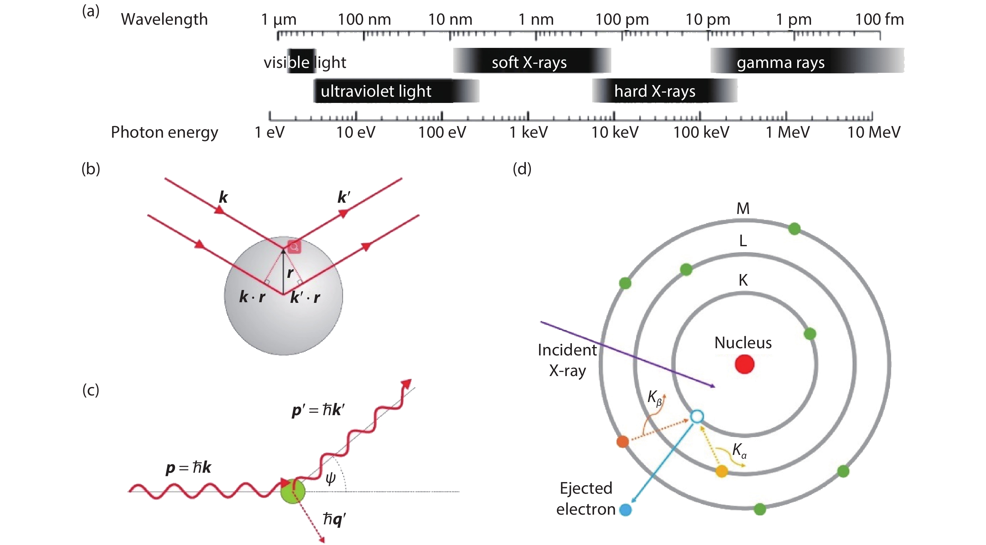
X-rays are electromagnetic waves with wavelengths ranging from 0.01 to 10 nm (Fig. 1(a)). From a quantum mechanical perspective, a beam of X-rays can be quantized into photons of which the photon energy is tens of thousands of times greater than that of visible light. The intensity of X-rays is then given by the number of photons passing through a given area per unit time. There are two ways of interaction between X-ray photon and matter: scattering and absorption.

Figure  1.  (Color online) (a) Spectrum region of X-ray to wavelength and photon energy. (b) Thomson scattering from an atom. An X-ray with a wave vector k scatters from an atom to the direction specified by k’. The scattering is assumed to be elastic. Reproduced with permission from Ref. [6]. (c) Compton scattering. A photon with energy ε=ck and momentum k scatters from an electron at rest with energy mc2. The electron recoils with a momentum q=(kk). Reproduced with permission from Ref. [6]. (d) Schematic diagram of photoelectric absorption process. An X-ray photon is absorbed and an electron ejected from the atom. The hole created in the inner shell (k) can be filled by Fluorescent X-ray emission. Electrons in an outer shell fill the hole, creating a photon. In this diagram the outer electron comes either from the L or M shell. In the former case the fluorescent radiation is referred to as the Kα line, and in the latter as Kβ line.

X-ray scattering can be divided into two types: Thomson scattering and Compton scattering. As shown in Fig. 1(b), Thomson scattering is elastic scattering of X-ray radiation by a free charged particle, which won’t change the kinetic energy and frequency of X-ray photon. Thomson scattering is also coherent and its coherence makes it exploited in investigations of the structure of materials. when Bragg’s law is fulfilled, the X-ray will be elastic scattered from a crystal and coherently add up, then the scattering is restricted to lie at points on the reciprocal lattice. On the contrary, Compton scattering (Fig. 1(c)) is inelastic and incoherent scattering where the energy of incident X-ray photon may be transferred to the electron, resulting in lower frequency of scattered photon relative to that of incident one. The unique information on the electronic structure of materials could be obtained by Compton scattering. As the energy of incident X-ray photon is increased, the scattering becomes progressively more inelastic for a given scattering angle[6], in other words, the Compton scattering gradually dominates the X-ray scattering as the energy of incident photon increases.

Fig. 1(d) illustrates the process of photoelectric absorption. After the incident X-ray photon is absorbed by an atom, the excess energy is transferred to an electron which will be ejected from the inner atom shell, creating a hole in that shell and leaving the atom ionized. The hole is subsequently filled by an electron from an outer shell with the simultaneous emission of a characteristic X-ray photon, of which the energy equals to the difference in the binding energies of electrons in these two shells. The characteristic emission X-ray is often used in X-ray fluorescence (XRF) analysis. By the way, the ionized atom could fill the hole in inner shell by expelling Auger electron as well.

The X-ray absorption can be quantitatively calculated by the following formula[6]:

I0I(d)I0=1eμd=1eσρd,

where the I0 and I(d) are the X-ray intensities when the thicknesses are zero and d, μ is the linear absorption coefficient, d is the thickness, σ is the X-ray absorption cross-section and ρ is the density of matter. The absorption cross-section σ is a function of X-ray photon energy (ε) and atomic number (Z), approximatively exhibiting the following relationship:

σZ4ε3.

It could be concluded that high energy X-ray has strong penetrating capability and the matter with heavy atoms is able to attenuate X-ray more efficiently. It is how the X-ray imaging is realized, and X-ray detection also puts forward some requirements to the detection materials for the same reason.

Direct detection is realized utilizing the ionization capacity of X-ray. When X-ray reaches a direct detector, the detecting materials are ionized, generating many free charges by the photoelectric effect and Compton scattering. In these two processes, the energy of X-ray photons is directly transferred to lots of charges, and then these excess charges are collected by electrodes under certain bias.

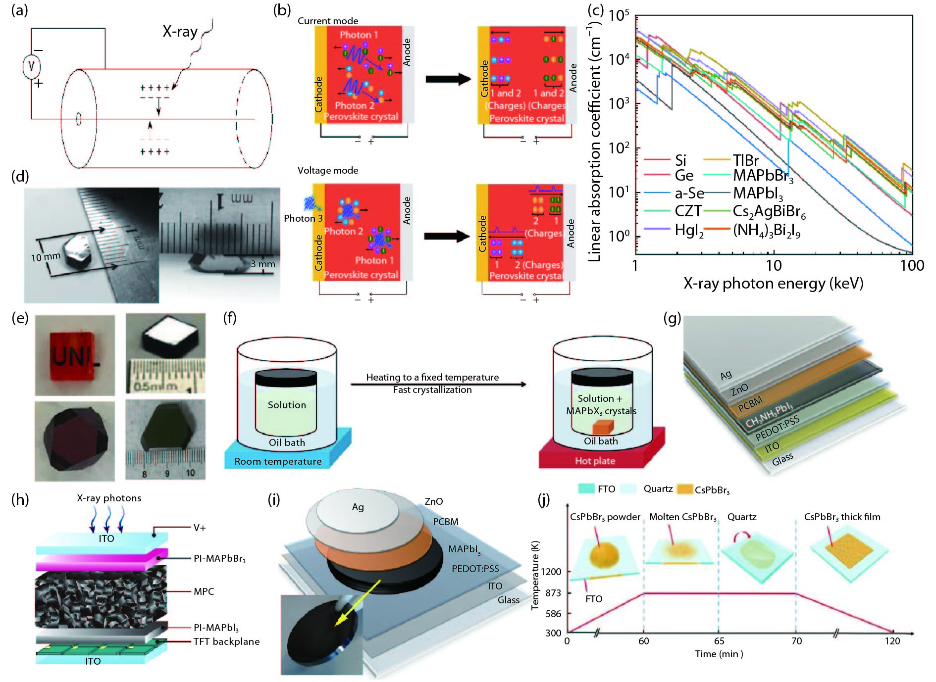
The gas-filled detector worked at the voltage of ionization region (100 to 200 V), which is known as ion chamber[22] (Fig. 2(a)), is a type of common and inexpensive X-ray detector. A typical ion chamber instrument contains a chamber of about 200 cm3 filled with ambient air. When X-ray is absorbed by the air contained by the chamber, charge pairs (a positive ion and an electron) are produced, which are collected and amplified for recording the signal produced. However, on account of the slow detection speed, large volume, low X-ray attenuation and feeblish response, the application fields of ion chamber are severely restricted, not suitable for imaging and energy spectrum analysis.

Figure  2.  (Color online) (a) Working Principle of ion chamber. Reproduced with permission from Ref. [22]. (b) Semiconductor X-ray detectors’ two types of work modes: current mode and voltage mode. Reproduced with permission from Ref. [23]. (c) The linear absorption coefficients of different kinds of perovskite and conventional X-ray detectors. (d) Images of a piece of MAPbI3 single crystal. Reproduced with permission from Ref. [52]. (e) Images of perovskite single crystals of MAPbBr3 (left top), c-MAPbI3 (right top), Cs2AgBiBr6 (left bottom) and (NH3)4Bi2I9 (right bottom). Reproduced with permission from Ref. [1618, 53]. (f) Schematic representation of the ITC apparatus in which the crystallization vial is immersed within a heating bath. The solution is heated from room temperature and kept at an elevated temperature (80 °C for MAPbBr3 and 110 °C for MAPbI3) to initiate the crystallization. Reproduced with permission from Ref. [54]. (g) Schematic of layer stacking of the MAPbI3-based PIN photodiode. Reproduced with permission from Ref. [20]. (h) Illustration of an all-solution-processed digital X-ray detector. Reproduced with permission from Ref. [21]. (i) Device stack of the MAPbI3-wafer-based X-ray detector. Inset: Free-standing MAPbI3 wafer (thickness: 1 mm). Reproduced with permission from Ref. [55]. (j) Preparation scheme for a thick CsPbBr3 film using the four-step hot-pressing method. Reproduced with permission from Ref. [56].

Direct X-ray semiconductor detector have become an attractive research field in recent years due to its good absorption, high sensitivity, fast response and excellent energy resolution[23]. Through the interaction of X-ray with semiconductor materials, electrons are excited from valence bands to high energy states, and then produce plenty of secondary electrons. These high energy electrons are rapidly thermalized to conduction band minimum generating pairs of electrons and holes. A bias voltage is applied across the semiconductor which causes these charge carriers to move, leading to a signal. The energy needed to produce an electron–hole pair (EHP) in a semiconductor is typically about 2–10 eV, which is considerably less than that required to produce ionizations in air, therefore, a relatively large number of charge carriers is produced for each photon absorbed[22]. As depicted in Fig. 2(b), semiconductor X-ray detector has two types of work modes: current mode and voltage mode[23]. The former one is always used for dose rate measurement or generating imaging contrast[11], while the latter one is applied to photon counters or energy spectroscopy of X-ray[24].

The direct X-ray detection is generally considered to consist of three processes: absorption of X-ray energy, generation of carries (EHPs) and transport of charges[9]. There are several parameters in these processes influencing the performance of semiconductor X-ray detectors.

In the first process, the atomic number (Z) and density (ρ) of the detection material determine the linear absorption coefficient (μ), which represents the X-ray stopping power of this material at per unit thickness under certain photon energy. Fig 2(c) shows the linear absorption coefficients of different kinds of perovskites and some conventional X-ray detecting materials. In order to maximize X-ray energy utilization and reduce the risk of radiation leakage, semiconductor layer needs sufficient thickness to completely absorb X-rays. However, larger thickness tends to cause undesirable problems. For example, it is difficult to fabricate large area thick film with high quality and the thick semiconductor has lower charge collection efficiency in most cases. Besides, a larger thickness can also damage the imaging quality of X-ray, because the lateral charge transport will cause signal crosstalk in the image read out circuit[25]. Hence, high Z and large ρ are essential for X-ray detection materials because they can decrease the X-ray absorption length.

In the carriers generation process, the EHP creation energy (W±), which is defined as the amount of radiation energy required to create a single EHP, should be as small as possible because the free charge (ΔQ) generated from an absorbed radiation of energy (ΔE) could be calculated by the following formula[11]:

ΔQ=eΔEW±,

where e is the elementary charge. W± is proportional to the bandgap (Eg) in many material systems. It is well-known that W± ≈ 3Eg for many crystalline semiconductors, which is so-called Klein rule[26, 27], so this means that the low Eg is beneficial to the carriers generation.

The transport and collection of carries is a pretty complicated process in semiconductor X-ray detector, and various of parameters are related. The central parameter is the product of carrier mobility and mean carrier lifetime (μτ), which is normally called the range of the carrier. It represents the mean distance drifted by the carrier per unit electric field before the carrier disappears by recombination (or trapped by defects)[11]. Since X-ray detector has much thicker film thickness than the visible light detector, the μτ greatly limits the sensitivity of detector by influencing charge collection efficiency, where sensitivity is an important parameter to measure the performance of the detector. Materials with strong X-ray stopping capacity, lower W±, high μτ product and high charge collection efficiency are needed to realize high-sensitivity devices. In same way, the larger electric field (bias voltage per unit thickness, F) applied on the X-ray detector can promote the output signal of X-ray detector as well, which improves the theoretical sensitivity during the detection process. When analyzing and comparing sensitivities, it is necessary to indicate the electric field applied across the device. But it doesn’t mean that a large F is absolutely beneficial for X-ray detection because F can affect another important parameter, dark current (Id). It affects the lowest detectable dose rate, in the unit of (μGyair/s or nGyair/s). The dark current should be as small as possible so as to obtain enough signal to noise ratio (SNR) and is normally attributed to two factors: injectied carriers from contacts and intrinsic thermally activated carriers The former is mainly caused by the electrical filed F and the resistivity of the material, while the latter is related to the Eg of semiconductor. In general, material with a broad bandgap likely has lower dark current, but the corresponding larger W± reduces the intrinsic X-ray sensitivity to some extent, which is quite paradoxical.

Since Van Heerden first investigated silver chloride (AgCl) crystals as radiation detectors in 1945[28], semiconductor X-ray detectors have made much progress. Due to the excellent transport ability of charges, high-purity silicon (Si) and germanium (Ge) have been widely applied in X-ray (or γ-ray) spectrum measurement[22, 29-33]. Nevertheless, the narrow bandgaps of Si and Ge crystals cause considerable thermal noise, which need to be suppressed by ancillary cooling systems or bulky cryogenics resulting in inconvenience of application[31]. In addition, the weak X-ray absorption capacity (due to the lower Z) and poor radiation intolerance of them are also limiting the applied areas. In comparison to monoatomic semiconductors, compound semiconductors offer more possibilities for direct X-ray detection because of the tunable bandgap and introduction of high-Z elements. The cadmium zinc telluride (Cd1–xZnxTe, x < 0.2, CZT) is typical case of compound semiconductors X-ray detectors[31, 32, 34]. Other semiconductor X-ray detectors have also realized fair performance based on HgI2[35-39], PbI2[37, 40, 41], PbO[25, 42], TlBr[43, 44] and so on.

In recent years, halide perovskites (composition of ABX3, X = Cl, Br or I) have revolutionized the development of compound semiconductor X-ray detectors due to many beneficial qualities of them. Firstly, each of common elements in halide perovskite material systems, e.g., Cs, Pb, Bi, Br and I, has a high Z, meaning a strong stopping power and a favorable absorption efficiency. Meanwhile, narrower bandgaps of halide perovskites give rise to smaller W±, which produce high intrinsic X-ray sensitivity. Furthermore, perovskites own outstanding charge transportation ability (long carrier lifetime and low trap density), leading to their μτ products much better than that of conventional compound semiconductor X-ray detectors[45]. Table 1 summarizes the various parameters of part of conventional and most of perovskites X-ray direct detectors in researches through the years.

Table  1.  Performances and parameters of part of conventional and perovskite X-ray direct detectors. In “status” column, A is amorphous, S is single-crystal and P is polycrystalline.
MaterialLinear absorption coefficients to
50 keV (cm−1)
W± (eV)μτ (cm2 V−1)F (V/cm)Sensitivity (μC/(Gy·cm2))Lowest detectable dose rate (nGyair/s)Status (A, P or S)Ref.
μeτeμhτh
Si1.0223.62> 1~ 10.58< 8300S[30-32, 71]
CZT60.63~ 4.610−3 – 10−210−50.1−131850S[32, 34, 72, 73]
a-Se3.864453 × 10−7
10−5
10−6
6 × 10⁻⁵
> 10420A[11, 21, 57]
MAPbBr319.416.031.2 × 10−20.580500S[16]
MAPbBr3(Si)19.416.031.39 × 10−4~ 352.1 × 10⁴< 100S[19]
MAPbBr3(PIN)19.416.031502.36 × 104S[59]
MAPbI3(Cuboid)40.61~ 4.41.1 × 10−410968.9S[53]
MAPbI3(GA alloyed)< 40.61~ 4.51.25 × 10−2~ 422.3 × 10416.9S[60]
CsPbBr3(QDs)35.07~ 5.910001450S[62]
CsPbBr3(Rb doped)35.07~ 5.97.2 × 10−4~ 2008.1 × 103S[63]
CsPbI3(1D)57.06~ 6.83.63 × 10−341.72.37 × 103219S[64]
Cs2AgBiBr639.085.611.21 × 10−3, 6.3 × 10⁻³, 5.51 × 10⁻³, 1.94 × 10⁻³, —, 5.95 × 10−333, 250, 5000, 227, 500, 5004.2, 105, 250, 288.8, 988,1974S/P[17, 18, 63, 66-68]
(NH4)3Bi2I946.985.471.1 × 10−2//, 4 × 10−3508.2 × 103//, 803⊥55S[18]
(DMEDA)BiI5~ 405.15494072.5S[69]
MAPbI3(PV)40.61~ 4.42 × 10⁻⁷~ 80001.75P[20]
MAPbI3(Flat detector)40.61~ 4.41 × 10⁻⁴~ 24103.8 × 103P[21]
MAPbI3(Wafer)40.61~ 4.42 × 10−457002.527 × 103P[55]
CsPbBr3(Hot-pressed)35.07~ 61.32 × 10−2505.5684 × 104215P[56]
MA3Bi2I9~405.391.2 × 10−3 (out-of-plane), 2.8 × 10⁻³ (in plane)12010 620 (out-of-plane)5.3S[74]
DownLoad: CSV  | Show Table

In addition to their superior performances, solution-processed perovskites have another significant advantage, i.e. the low cost both in raw materials and manufacturing techniques[46, 47], which provides more chance for cosmically commercialization of perovskite X-ray detectors. Perovskites also surprisingly perform well in radiation tolerance and self-healing[48, 49], which is explained by the defect tolerance (or defect relaxation)[23, 50, 51].

Single crystal is quite infrequent in the past compound semiconductor X-ray detectors, because the single crystal growth process of other materials is often expensive and hard to obtain a bulk of big enough single crystal for flat panel imaging. But now in perovskites, this situation has been changed. Dong et al. have successfully fabricated organolead trihalide perovskite (OTP) single crystal (MAPbI3, MA = CH3NH3) with long carrier diffusion lengths (> 175 μm) by low-cost solution-grown method in 2015[52]. The length of this single crystal is about 10 mm, while the thickness of that is 3 mm, as shown in Fig. 2(d). The excellent μτ product, high-Z elements and low-cost growth method all imply the exciting prospects of perovskite single crystals applied in X-ray detection. As expected, it was soon reported that a highly sensitive X-ray detector with a record-high μτ product (1.2 × 10⁻² cm2 V−1) was made by MAPbBr3 single crystal[16]. The sensitivity of this detector (80 μC/(Gy·cm2)) is even four times higher than the sensitivity achieved with a-Se X-ray detectors[57] and this work then intrigued many researchers[58]. Further research from this team realized simple X-ray imaging and improved the sensitivity of MAPbBr3 single crystal X-ray detector to 2.1 × 10⁴ μC/(Gy·cm2) by noise current suppression and applying higher working voltage[19]. Another device structure design strategy for X-ray imaging was put forward as PIN diode array, and the sensitivity of this detector based on MAPbBr3 single crystal attained 2.36 × 10⁴ μC/(Gy·cm2)[59].

Compared with MAPbBr3 single crystal, X-ray detector made by MAPbI3 single crystal is rather limited although its X-ray stopping power is stronger. Ye et al. thought it was probably because the natural geometry of MAPbI3 single crystals is usually nonrectangular dodecahedrons, which is not as feasible as cuboid-shaped single crystals (such as MAPbBr3) for device fabrications, especially for flat-panel array[53]. They demonstrated high-quality cuboid-MAPbI3 single crystals by seed dissolution-regrowth (SDR) method and manufactured an X-ray detector with a favorable sensitivity. Moreover, Huang et al. used A-site cation engineering decreasing the electron-phonon coupling strength and increasing the material defect formation energy in MAPbI3 single crystals, improved the charge collection efficiency and gained a highly efficient X-ray detector[60]. Unlike organic-inorganic hybrid perovskites, all-inorganic perovskites (such as CsPbBr3) have attracted interest of people mainly because of their stability[61], and the replacement of organic A-site cation by metal cation (Cs+) also leads to better absorption efficiency for X-ray. A flexible, printable X-ray detectors based on CsPbBr3 quantum dots (QDs) has been made[62]. Some other preliminary works making good advances have also been reported about rubidium (Rb) doped CsPbBr3 single crystal[63] and one-dimensional CsPbI3[64] X-ray detectors.

Because Pb2+ can severely damage the human brain and threaten the biological systems for the high solubility in water, the toxicity of lead halide perovskites should not be neglected[17]. Therefore, the bismuth (Bi) halide perovskites have become promising materials for X-ray detection[65]. Bi3+ has the same electronic configurations with Pb2+ and has higher atomic number (83 for Bi) that will benefit the attenuation of X-ray. A typical material of these is Cs2AgBiBr6 double perovskite, which was first reported in 2017 as X-ray detectors showing an adequate low-dose X-ray detection ability (lowest detection limit: 59.7 nGy/s)[17]. This performance may be attributed to its high intrinsic resistivity and consequent low dark current. The familiar ionic migration in perovskite crystals will cause large noise and baseline drift limiting the detection and performance of X-ray, hence Yang et al. introduced bismuth oxybromide (BiOBr) as heteroepitaxial passivation layers to suppress ionic migration in Cs2AgBiBr6 polycrystalline wafer, decrease noises and improve sensitivity[18]. Centering on Cs2AgBiBr6 single crystal systems, multifarious approaches, such as liquid-nitrogen refrigeration[66], A-site cation engineering[67], management of crystallization temperature[68] and improved ordering of crystal structure[63], have been attempted to promote the performance of X-ray detection.

In addition to double perovskites, another low-dimensional and bismuth halide perovskite materials system has also received attention due to its unique anisotropic performance. Zhuang et al. showed their 2D layered perovskite-like (NH4)3Bi2I9 X-ray detector revealing high sensitivity of 8.2 × 10³ μC/(Gy·cm2) in the parallel direction and low detection limit of 55 nGy/s in the perpendicular direction[18]. The well performance might be ascribed to the suppression of ionic migration by the unique 2D crystal construction, reducing noise in device. Recently, X-ray detectors made by (DMEDA)BiI5 (DMEDA: N,N'-dimethylethanediamine) and (H2MDAP)BiI5 (H2MDAP = N-methyl-1,3-diaminopropanium) with one-dimensional crystal structure have been reported and achieved fair X-ray detection sensitivities[69, 70].

Fig. 2(e) shows some graphs of single crystals among part of representative perovskites discussed above, and Fig. 2(f) schematically illustrates the method of inverse temperature crystallization (ITC), which is a common and low-cost method for synthesis of perovskite single crystals[54]. In a word, perovskite single crystals have guided a new development direction for X-ray detection relying on their outstanding detecting performance.

Actually, the first time of polycrystalline perovskites X-ray detection was before that of single crystal detection. Even so the material systems of polycrystalline perovskites X-ray detection have been hardly innovated, while the fabrication technique of large-area polycrystalline perovskite thick films for X-ray imaging has made great progress. Yakunin et al. firstly tried to detect X-ray and carry out X-ray imaging using a piece of polycrystalline perovskite solar cell (Fig. 2(g))[20]. In order to absorb X-ray as much as possible, they manufactured MAPbI3 photovoltaic cells with thick perovskite layers (up to about 700 nm) by spin-coating method, then obtained X-ray detectors with sensitivity of 1.75 μC/(Gy·cm2) and lastly received X-ray images by using this single-pixel detector and moving the object with an xy positioner[47]. In view of the low efficiency of taking X-ray images, Kim et al. designed a new device structure of perovskite layers especially for X-ray detection (Fig. 2(h)) and realized large-area, low-dose X-ray imaging[21]. Two interlayers of polyimide (PI)-perovskite composites were inserted by spin-casting as hole-transporting or blocking layers to reduce the dark current caused by charge injection. The high intrinsic resistivity of PI could also reduce electrical crosstalk among the pixels. The 830-μm-thick polycrystalline MAPbI3 photoconductor layer was printed on the coated PI-MAPbI3 using a doctor blade. Finally, tape-automated bonding of readout integrated circuits was performed on the X-ray detectors. The imaging area of this X-ray digital flat detector consisted of 1428 × 1428 pixels (10 × 10 cm2) with a pixel pitch of 70 μm and accomplished low-dose imaging down to 10 μGy.

In addition, two crafts have been presented for potential fabrication of large-area and high-quality polycrystalline perovskite thick films applied in X-ray imaging. The first one is a mechanical sintering process to fabricate polycrystalline MAPbI3 wafers with millimeter-scale thickness and well-defined crystallinity (Fig. 2(i))[55]. It could be found that the performances of MAPbI3 films were obviously elevated by their additional structure design of layers, as Fig. 2(j) shown. The second one is a hot-pressing method to fabricate thick quasi-monocrystalline CsPbBr3 films (Fig. 2(k)), and a record sensitivity of 55684 μC/(Gy·cm2) is achieved[56]. The hot-pressing method is simple and can produce thick quasi-monocrystalline CsPbBr3 films with uniform orientations and large μτ product.

Spatial resolution is a vital performance of an X-ray imaging system. While the spatial resolution of imaging system promoted, the clearer X-ray images would be collected. The spatial resolution of the imaging system can be determined with the modulation transfer function (MTF), representing the transfer ability of input signal modulation of the spatial frequency (in line pair per millimeter; lp/mm or cycles per millimeter; cy/ mm) relative to its output[21]. An MTF value of 1 indicates the perfect detection of a given spatial frequency. To compare different detectors, it is practicable to determine the value of the spatial frequency at which the MTF drops to 0.2[75].

The slanted-edge method is frequently used to measure the curve of MTF[76]. Through processing the X-ray image of a sharp, attenuating edge device (lead foil with sharp edge, Fig. 3(a)), the edge spread function (ESF) information could be obtained. The ESF is then differentiated to get the line spread function (LSF) and the MTF similarly deduced by Fourier transformation, as the following relationship:

Figure  3.  (Color online) (a) X-ray image of resolution test chart. Reproduced with permission from Ref. [42]. (b) An edge X-ray image used for calculation of MTF. Reproduced with permission from Ref. [76]. (c) A simplified schematic diagram of the cross section of a single pixel with a TFT. The charges generated by the absorption of X-rays drift towards their respective electrodes. The TFT is normally off and is turned on when the gate G1 is addressed. Reproduced with permission from Ref. [11]. (d) Idealized MTF and MTF due to trapping. Reproduced with permission from Ref. [25].
MTF(f)=F(LSF(x))=F(dESF(x)x),

where x is the position of pixel and f is the spatial frequency. Another approach to determine MTF is very visualized, which is to take X-ray image for an X-ray resolution test chart. As shown in Fig. 3(b), this test chart made by lead film consists of many line pairs with different intervals, representing a series of spatial frequencies from low to high. The MTF of X-ray system can be estimated by observing the definition at each spatial frequency.

The most common X-ray imaging system by direct detection is flat panel X-ray imager (FPXI)[11], which is widely used in medical diagnosis, such as mammography. An FPXI consists of a large array of pixels, and each pixel has a thin film transistor (TFT) to read out the signal. This array is coated by a suitable X-ray detection material, which is then coated with electrodes on its surface to allow the application of a bias voltage. Thus, each pixel acts as an individual X-ray detector and has a biased semiconductor as illustrated in the schematic cross section of a pixel depicted in Fig. 3(c).

The spatial resolution of direct FPXI is usually much higher than that of indirect X-ray imaging system because the X-ray is not scattered but scintillation is strongly scattered in scintillators. The theoretical limit of the MTF for an FPXI is a two-dimensional sinc function in diagonal direction dominated by the pixel aperture (a)[77], as the following formula:

MTF(f)=sinc2(af2),

where f is the spatial frequency. Based on the idealized situation, several factors are influencing the MTF of direct FPXI. The design of FPXI generally allows only one type of carriers (electron or hole) to be collected by TFTs[11], and the trapping of this type of carriers (such as hole in a-Se) will give rise to the degrading of MTF[78]. Kabir has created a model to investigate this phenomenon (Fig. 3(d))[25]. For some materials, the K-fluorescence reabsorption mechanism also reduces MTF, i.e., the K-edge characteristic X-ray photon is reabsorbed in a region away from the initial X-ray interaction point and hence causes blurring[79]. Besides, the lateral diffusion of carriers would spread or blur the information especially in FPXIs based on crystalline or polycrystalline semiconductors[11, 21, 80].

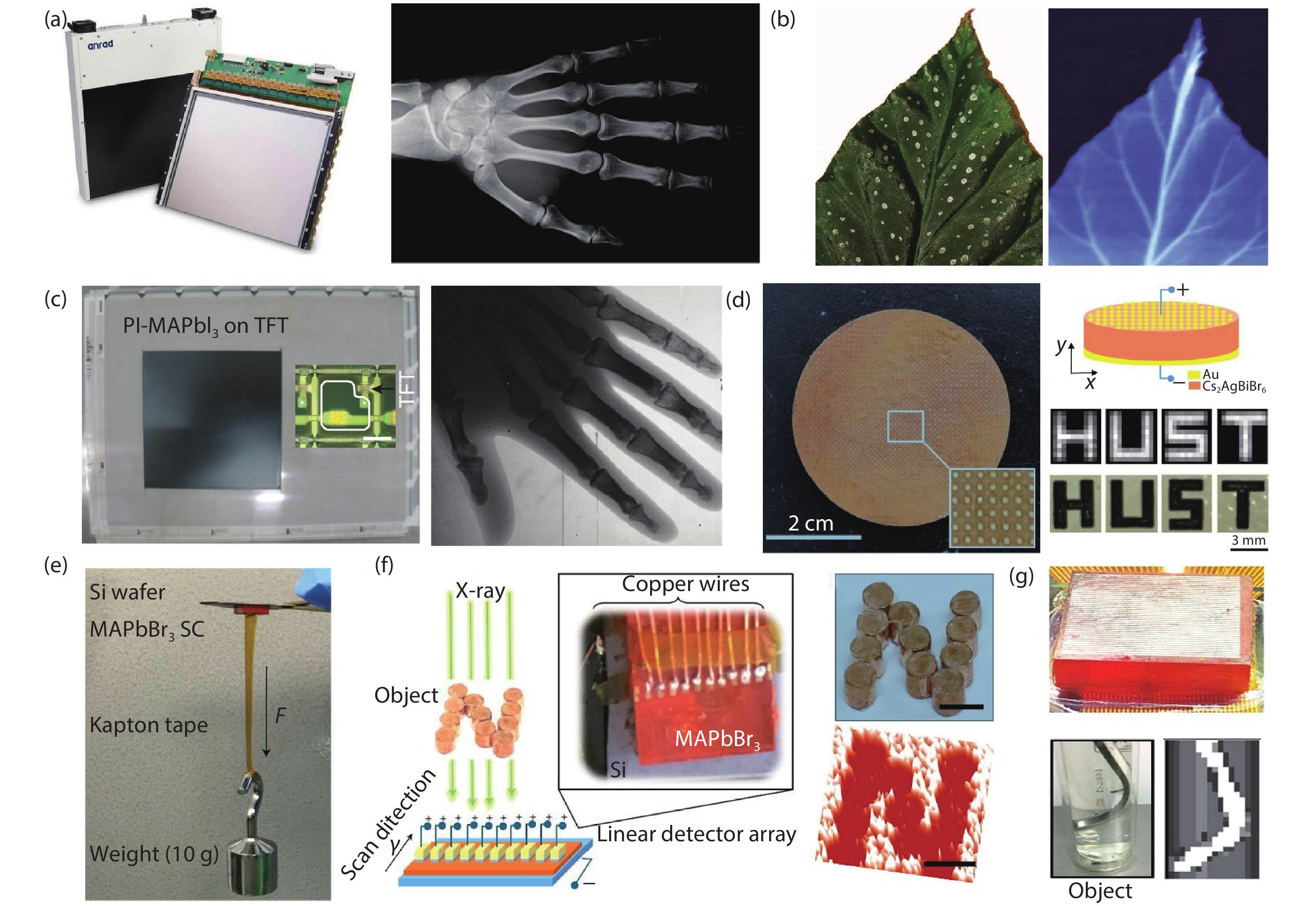
In current commercial direct FPXIs, the material of choice is stabilized amorphous selenium (a-Se)[11], which is easy to integrate on large-area TFT back plate and has low dark current to reach adequate SNR under high work voltage. Fig. 4(a) demonstrates an a-Se based FPXI (AXS-2430) for mammography that has been developed and marketed by Anrad and the corresponding X-ray image of a hand taken by this FPXI. However, the practical applications of a-Se imager are still very limited, because of its low X-ray stopping power, deficient μτ product value, and the accompanying high operating electrical fields required to overcome its poor charge collection efficiency (Table 1)[21].

Figure  4.  (Color online) (a) Left: Anrad’s mammographic FPXI (AXS-2430) is used in mammography markets. The field of view is 24 × 30 cm2 and the FPXI have a pixel pitch of 85 μm. Right: an X-ray image of a hand from AXS-2430. Reproduced with permission from Ref. [11]. (b) Photograph (left) and corresponding X-ray image (right) of a leaf, obtained with the photoconductor in Ref. [20]. Reproduced with permission from Ref. [20]. (c) Left: image of spin-cast PI-MAPbI3 on an a-Si:H TFT backplane. The inset in the left shows a single-pixel structure of TFT (scale bar 30 μm). Right: A hand X-ray image obtained from this MAPbI3 FPXI. Reproduced with permission from Ref. [21]. (d) Left: The fabricated multi-pixel wafer-based Cs2AgBiBr6 polycrystalline detector. Right top: schematic illustration of the imaging process. Right bottom: X-ray image and optical image of ‘HUST’ symbol. Reproduced with permission from Ref. [18]. (e) Photograph of Si-integrated MAPbBr3 single crystal with a 10 g weight attached to the MAPbBr3 crystal. Reproduced with permission from Ref. [19]. (f) Left: schematic illustration of X-ray imaging with Si-integrated MAPbBr3 single crystal detectors. Right: photo (top) and X-ray image (bottom) of an ‘N’ copper logo. Reproduced with permission from Ref. [19]. (g) Top: photo of the PIN array. Bottom: object photo (left) and X-ray image (right) for 100 keV energy. Reproduced with permission from Ref. [59].

As described above in Section 3.3, direct X-ray imaging demonstrations based on perovskite have been achieved by various means. Yakunin et al. used a MAPbI3 based solar cell as a single-pixel X-ray detector, carried out scanning of the object and demonstrated a simple X-ray image of piece of leaf (Fig. 4(b))[20]. Though this imaging method was ineffective and the quality was poor, this work had certainly inspired other researchers.

Kim et al. referred the design philosophy of a-Se FPXIs, firstly manufactured a true sense of perovskite-based FPXI and successfully realized large-area X-ray imaging[21]. In this work, a demonstrative X-ray image of human hand was taken by this FPXI (Fig. 4(c)) under a low radiation dose (25 μGy) and the spatial resolution reached 3.1 lp/mm when MTF dropped to 0.2. This value was unsatisfying compared with that of a-Se FPXI (7.1 lp/mm at MTF = 0.2), and they speculated it to MAPbI3 crystallites of 20 to 100 μm size that are larger than a pixel size and can overlap adjacent pixels, leading to charge sharing among pixels.

In addition, Yang et al. fabricated a large-area (5 cm of diameter) Cs2AgBiBr6 polycrystalline wafer by the isostatic-pressing process, then Au electrodes array was thermally evaporated on the wafer to accomplish preliminary X-ray imaging (6 × 6 array, Fig. 4(d))[18]. In this work, MTF was measured as 4.9 lp/mm when MTF value was equal to 0.2 by point-scanning method without read out integrated circuit (ROIC).

On the other hand, X-ray imaging attempts by means of perovskite single crystals have made some good advances as well. Wei et al. reported a low-temperature solution-processed molecular bonding method with the assistance of brominated APTES molecules[19]. They firmly integrated MAPbBr3 single crystal with Si wafer by utilizing this method (Fig. 4(e)), which made the perovskite single-crystal FPXI possible. Then the X-ray image of ‘N’ copper logo was taken by this integrated Si-perovskite single crystal on which ten pixel electrodes (linear array with pixel size of 200 μm and a pitch of 400 μm) were deposited (Fig. 4(f)). During the imaging process, the object was scanning by the linear detection array. Inspired by this design, Wang et al. decided to fabricate PIN diodes array on MAPbBr3 single crystal, attaining X-ray images under different X-ray photon energies (Fig. 4(g))[59].

From this review, it could be seen that direct-type perovskite X-ray detection and imaging have revealed vast potentials for future applications. Compared to a-Se, perovskite semiconductor has many significant advantages including strong X-ray stopping power, remarkable carrier transport ability, high intrinsic sensitivity, low detection limit and inexpensive solution-processed fabrication. However, there still exist some issues to be addressed to facilitate the commercialization.

Firstly, more physical insights are encouraged to understand and guide the material optimization and device design in order to fulfill high sensitivity and low noise. For example, the narrower bandgap leads to smaller W±, and higher intrinsic X-ray sensitivity, while the broader bandgap material usually gives larger resistance and therefore lower noise. Hence, an optimal bandgap needs to be selected for the sake of balancing sensitivity and noise, after all, the X-ray imaging requires adequate SNR with as low dose as possible. We might overemphasized on high sensitivity while ignored the noise reduction, particularly those devices with large trap-assisted photoconductive gains, they might not be so useful for practical applications, because the noises are also increased because of the traps, and ultimately the SNRs are sacrificed. Secondly, it is important to understand and identify the factors that limit the special resolution of the X-ray imaging. It was found that perovskite-based FPXI had much lower spatial resolution than that of a-Se[21], but the reason was not clear yet. Trapping and lateral diffusion of carriers in polycrystalline perovskite film are inferred as probable origins. The promotion of spatial resolution in perovskite FPXI is an important aim in next stage. Thirdly, low-cost method to fabricate large-area high-quality perovskite thick film (~ 1 mm) should be further explored. Some of the previous methods required high temperature, which not only increased the processing difficulty but also made them questionable when integrating with α-Si TFT back panel[19]. Fourthly, new perovskite derivatives are worthy to be explored, such as double perovskites and low-dimension perovskites[17, 18], which are able to provide new possibilities for the performance improvement for X-ray detection and imaging. In addition, the radiation hardness of perovskite X-ray detector is also an important factor. There are a few very encouraging results on perovskite radiation stability reported[49]. However, more data related with radiation hardness are certainly encouraged, and the testing methods need to be standardized.

In conclusion, more efforts should be contributed to the theorical understanding, fabrication methods and attempting of new materials for perovskite direct X-ray detectors. We believe that the perovskites will emerge as a splendid X-ray detecting material and hold a bright future for practical X-ray imaging applications.


[1]
Spahn M. X-ray detectors in medical imaging. Nucl Instrum Methods Phys Res A, 2013, 731, 57 doi: 10.1016/j.nima.2013.05.174
[2]
Van Eijk C W. Inorganic scintillators in medical imaging. Phys Med Biol, 2002, 47, R85 doi: 10.1088/0031-9155/47/8/201
[3]
Duan X, Cheng J, Zhang L, et al. X-ray cargo container inspection system with few-view projection imaging. Nucl Instrum Methods Phys Res A, 2009, 598, 439 doi: 10.1016/j.nima.2008.08.151
[4]
Haff R P, Toyofuku N. X-ray detection of defects and contaminants in the food industry. Sens Instrum Food Quality Safety, 2008, 2, 262 doi: 10.1007/s11694-008-9059-8
[5]
Chapman H N, Fromme P, Barty A, et al. Femtosecond X-ray protein nanocrystallography. Nature, 2011, 470, 73 doi: 10.1038/nature09750
[6]
Nielsen J A, McMorrow D. Elements of modern X-ray physics. Wiley, 2011
[7]
Moses W W. Scintillator requirements for medical imaging. LBNL Publications, 1999
[8]
Lin E C. Radiation risk from medical imaging. In: Mayo Clinic Proceedings. Elsevier, 2010, 1142
[9]
Knoll G F. Radiation detection and measurement. John Wiley & Sons, 2010
[10]
Rowlands J A. Medical imaging: Material change for X-ray detectors. Nature, 2017, 550, 47 doi: 10.1038/550047a
[11]
Kasap S, Frey J B, Belev G, et al. Amorphous and polycrystalline photoconductors for direct conversion flat panel X-ray image sensors. Sensors, 2011, 11, 5112 doi: 10.3390/s110505112
[12]
Zheng X, Chen B, Dai J, et al. Defect passivation in hybrid perovskite solar cells using quaternary ammonium halide anions and cations. Nat Energy, 2017, 2, 17102 doi: 10.1038/nenergy.2017.102
[13]
Xiao Z, Kerner R A, Zhao L, et al. Efficient perovskite light-emitting diodes featuring nanometre-sized crystallites. Nat Photonics, 2017, 11, 108 doi: 10.1038/nphoton.2016.269
[14]
Saliba M, Wood S M, Patel J B, et al. Structured organic–inorganic perovskite toward a distributed feedback laser. Adv Mater, 2016, 28, 923 doi: 10.1002/adma.201502608
[15]
Dou L, Yang Y M, You J, et al. Solution-processed hybrid perovskite photodetectors with high detectivity. Nat Commun, 2014, 5, 5404 doi: 10.1038/ncomms6404
[16]
Wei H, Fang Y, Mulligan P, et al. Sensitive X-ray detectors made of methylammonium lead tribromide perovskite single crystals. Nat Photonics, 2016, 10, 333 doi: 10.1038/nphoton.2016.41
[17]
Pan W, Wu H, Luo J, et al. Cs2AgBiBr6 single-crystal X-ray detectors with a low detection limit. Nat Photonics, 2017, 11, 726 doi: 10.1038/s41566-017-0012-4
[18]
Zhuang R, Wang X, Ma W, et al. Highly sensitive X-ray detector made of layered perovskite-like (NH4)3Bi2I9 single crystal with anisotropic response. Nat Photonics, 2019, 13, 602 doi: 10.1038/s41566-019-0466-7
[19]
Wei W, Zhang Y, Xu Q, et al. Monolithic integration of hybrid perovskite single crystals with heterogenous substrate for highly sensitive X-ray imaging. Nat Photonics, 2017, 11, 315 doi: 10.1038/nphoton.2017.43
[20]
Yakunin S, Sytnyk M, Kriegner D, et al. Detection of X-ray photons by solution-processed lead halide perovskites. Nat Photonics, 2015, 9, 444 doi: 10.1038/nphoton.2015.82
[21]
Kim Y C, Kim K H, Son D Y, et al. Printable organometallic perovskite enables large-area, low-dose X-ray imaging. Nature, 2017, 550, 87 doi: 10.1038/nature24032
[22]
Martin J E. Physics for radiation protection: a handbook. John Wiley & Sons, 2006
[23]
Wei H, Huang J. Halide lead perovskites for ionizing radiation detection. Nat Commun, 2019, 10, 1066 doi: 10.1038/s41467-019-08981-w
[24]
Devanathan R, Corrales L R, Gao F, et al. Signal variance in gamma-ray detectors—A review. Nucl Instrum Methods Phys Res A, 2006, 565, 637 doi: 10.1016/j.nima.2006.05.085
[25]
Kabir M. Effects of charge carrier trapping on polycrystalline PbO X-ray imaging detectors. J Appl Phys, 2008, 104, 074506 doi: 10.1063/1.2990765
[26]
Klein C A. Bandgap dependence and related features of radiation ionization energies in semiconductors. J Appl Phys, 1968, 39, 2029 doi: 10.1063/1.1656484
[27]
Alig R, Bloom S. Electron-hole-pair creation energies in semiconductors. Phys Rev Lett, 1975, 35, 1522 doi: 10.1103/PhysRevLett.35.1522
[28]
van Heerden P J. The crystalcounter. Noord-Holl Uitg Mij, 1945
[29]
McKay K G. A. germanium counter. Phys Rev, 1949, 76, 1537 doi: 10.1103/PhysRev.76.1537
[30]
Guerra M, Manso M, Longelin S, et al. Performance of three different Si X-ray detectors for portable XRF spectrometers in cultural heritage applications. J Instrum, 2012, 7, C10004 doi: 10.1088/1748-0221/7/10/C10004
[31]
Owens A, Peacock A. Compound semiconductor radiation detectors. Nucl Instrum Methods Phys Res A, 2004, 531, 18 doi: 10.1016/j.nima.2004.05.071
[32]
Del Sordo S, Abbene L, Caroli E, et al. Progress in the development of CdTe and CdZnTe semiconductor radiation detectors for astrophysical and medical applications. Sensors, 2009, 9, 3491 doi: 10.3390/s90503491
[33]
Luke P, Rossington C, Wesela M. Low energy X-ray response of Ge detectors with amorphous Ge entrance contacts. IEEE Trans Nucl Sci, 1994, 41, 1074 doi: 10.1109/23.322861
[34]
Szeles C. CdZnTe and CdTe materials for X-ray and gamma ray radiation detector applications. Phys Status Solidi B, 2004, 241, 783 doi: 10.1002/pssb.200304296
[35]
Zentai G, Schieber M, Partain L, et al. Large area mercuric iodide and lead iodide X-ray detectors for medical and non-destructive industrial imaging. J Cryst Growth, 2005, 275, e1327 doi: 10.1016/j.jcrysgro.2004.11.105
[36]
Schieber M M, Zuck A, Melekhov L, et al. High-flux X-ray response of composite mercuric iodide detectors. In: Hard X-Ray, Gamma-Ray, and Neutron Detector Physics. International Society for Optics and Photonics, 1999, 296
[37]
Street R, Ready S, Van Schuylenbergh K, et al. Comparison of PbI2 and HgI2 for direct detection active matrix X-ray image sensors. J Appl Phys, 2002, 91, 3345 doi: 10.1063/1.1436298
[38]
Schieber M, Hermon H, Zuck A, et al. Thick films of X-ray polycrystalline mercuric iodide detectors. J Cryst Growth, 2001, 225, 118 doi: 10.1016/S0022-0248(01)00832-6
[39]
Zentai G, Partain L D, Pavlyuchkova R, et al. Mercuric iodide and lead iodide X-ray detectors for radiographic and fluoroscopic medical imaging In: Medical Imaging 2003: Physics of Medical Imaging. International Society for Optics and Photonics, 2003, 77
[40]
Yun M S, Cho S H, Lee R, et al. Investigation of PbI2 film fabricated by a new sedimentation method as an X-ray conversion material. Jpn J Appl Phys, 2010, 49, 041801 doi: 10.1143/JJAP.49.041801
[41]
Shah K, Street R, Dmitriyev Y, et al. X-ray imaging with PbI2-based a-Si: H flat panel detectors. Nucl Instrum Methods Phys Res A, 2001, 458, 140 doi: 10.1016/S0168-9002(00)00857-3
[42]
Simon M, Ford R, Franklin A, et al. Analysis of lead oxide (PbO) layers for direct conversion X-ray detection. IEEE Symposium Conference Record Nuclear Science, 2004, 4268
[43]
Destefano N, Mulato M. Influence of multi-depositions on the final properties of thermally evaporated TlBr films. Nucl Instrum Methods Phys Res A, 2010, 624, 114 doi: 10.1016/j.nima.2010.09.006
[44]
Hitomi K, Kikuchi Y, Shoji T, et al. Improvement of energy resolutions in TlBr detectors. Nucl Instrum Methods Phys Res A, 2009, 607, 112 doi: 10.1016/j.nima.2009.03.129
[45]
Brenner T M, Egger D A, Kronik L, et al. Hybrid organic–inorganic perovskites: low-cost semiconductors with intriguing charge-transport properties. Nat Rev Mater, 2016, 1, 15007 doi: 10.1038/natrevmats.2015.7
[46]
de Arquer F P G, Armin A, Meredith P, et al. Solution-processed semiconductors for next-generation photodetectors. Nat Rev Mater, 2017, 2, 16100 doi: 10.1038/natrevmats.2016.100
[47]
Kasap S. Low-cost X-ray detectors. Nat Photonics, 2015, 9, 420 doi: 10.1038/nphoton.2015.108
[48]
Lang F, Nickel N H, Bundesmann J, et al. Radiation hardness and self-healing of perovskite solar cells. Adv Mater, 2016, 28, 8726 doi: 10.1002/adma.201603326
[49]
Yang S, Xu Z, Xue S, et al. Organohalide lead perovskites: more stable than glass under gamma-ray radiation. Adv Mater, 2019, 31, 1805547 doi: 10.1002/adma.201805547
[50]
Huang J, Yuan Y, Shao Y, et al. Understanding the physical properties of hybrid perovskites for photovoltaic applications. Nat Rev Mater, 2017, 2, 17042 doi: 10.1038/natrevmats.2017.42
[51]
Lang F, Shargaieva O, Brus V V, et al. Influence of radiation on the properties and the stability of hybrid perovskites. Adv Mater, 2018, 30, 1702905 doi: 10.1002/adma.201702905
[52]
Dong Q, Fang Y, Shao Y, et al. Electron–hole diffusion lengths > 175 μm in solution-grown CH3NH3PbI3 single crystals. Science, 2015, 347, 967 doi: 10.1126/science.aaa5760
[53]
Ye F, Lin H, Wu H, et al. High-quality cuboid CH3NH3PbI3 single crystals for high performance X-ray and photon detectors. Adv Funct Mater, 2019, 29, 1806984 doi: 10.1002/adfm.201806984
[54]
Saidaminov M I, Abdelhady A L, Murali B, et al. High-quality bulk hybrid perovskite single crystals within minutes by inverse temperature crystallization. Nat Commun, 2015, 6, 1 doi: 10.1038/ncomms8586
[55]
Shrestha S, Fischer R, Matt G J, et al. High-performance direct conversion X-ray detectors based on sintered hybrid lead triiodide perovskite wafers. Nat Photonics, 2017, 11, 436 doi: 10.1038/nphoton.2017.94
[56]
Pan W, Yang B, Niu G, et al. Hot-pressed CsPbBr3 quasi-monocrystalline film for sensitive direct X-ray detection. Adv Mater, 2019, 31, 1904405 doi: 10.1002/adma.201904405
[57]
Kasap S. X-ray sensitivity of photoconductors: application to stabilized a-Se. J Phys D, 2000, 33, 2853 doi: 10.1088/0022-3727/33/21/326
[58]
Heiss W, Brabec C. X-ray imaging: Perovskites target X-ray detection. Nat Photonics, 2016, 10, 288 doi: 10.1038/nphoton.2016.54
[59]
Wang X, Zhao D, Qiu Y, et al. PIN diodes array made of perovskite single crystal for X-ray imaging. Phys Status Solidi RRL, 2018, 12, 1800380 doi: 10.1002/pssr.201800380
[60]
Huang Y, Qiao L, Jiang Y, et al. A-site cation engineering for highly efficient MAPbI3 single-crystal X-ray detector. Angew Chem Int Ed, 2019, 58, 17834 doi: 10.1002/anie.201911281
[61]
Eperon G E, Paterno G M, Sutton R J, et al. Inorganic caesium lead iodide perovskite solar cells. J Mater Chem A, 2015, 3, 19688 doi: 10.1039/C5TA06398A
[62]
Liu J, Shabbir B, Wang C, et al. Flexible, printable soft-X-ray detectors based on all-inorganic perovskite quantum dots. Adv Mater, 2019, 31(30), 1901644 doi: 10.1002/adma.201901644
[63]
Yuan W, Niu G, Xian Y, et al. In situ regulating the order–disorder phase transition in Cs2AgBiBr6 single crystal toward the application in an X-ray detector. Adv Funct Mater, 2019, 29, 1900234 doi: 10.1002/adfm.201900234
[64]
Zhang B, Liu X, Xiao B, et al. High performance X-ray detection based on one-dimensional inorganic halide perovskite CsPbI3. J Phys Chem Lett, 2020, 11, 43 doi: 10.1021/acs.jpclett.9b03523
[65]
Wu C, Zhang Q, Liu G, et al. From Pb to Bi: a promising family of Pb-free optoelectronic materials and devices. Adv Energy Mater, 2019, 10, 1902496 doi: 10.1002/aenm.201902496
[66]
Steele J A, Pan W, Martin C, et al. Photophysical pathways in highly sensitive Cs2AgBiBr6 double-perovskite single-crystal X-ray detectors. Adv Mater, 2018, 30, 1804450 doi: 10.1002/adma.201804450
[67]
Xu Z, Liu X, Li Y, et al. Exploring lead-free hybrid double perovskite crystals of (BA)2CsAgBiBr7 with large mobility-lifetime product toward X-ray detection. Angew Chem Int Ed, 2019, 58, 15757 doi: 10.1002/anie.201909815
[68]
Yin L, Wu H, Pan W, et al. Controlled cooling for synthesis of Cs2AgBiBr6 single crystals and its application for X-ray detection. Adv Opt Mater, 2019, 7, 1900491 doi: 10.1002/adom.201900491
[69]
Yao L, Niu G, Yin L, et al. Bismuth halide perovskite derivatives for direct X-ray detection. J Mater Chem C, 2020, 8, 1239 doi: 10.1039/C9TC06313G
[70]
Tao K, Li Y, Ji C, et al. A lead-free hybrid iodide with quantitative response to X-ray radiation. Chem Mater, 2019, 31, 5927 doi: 10.1021/acs.chemmater.9b02263
[71]
Rikner G, Grusell E. Effects of radiation damage on p-type silicon detectors. Phys Med Biol, 1983, 28, 1261 doi: 10.1088/0031-9155/28/11/006
[72]
Bellazzini R, Spandre G, Brez A, et al. Chromatic X-ray imaging with a fine pitch CdTe sensor coupled to a large area photon counting pixel ASIC. J Instrum, 2013, 8, C02028 doi: 10.1088/1748-0221/8/02/C02028
[73]
Ivanov Y M, Kanevsky V, Dvoryankin V, et al. The possibilities of using semi-insulating CdTe crystals as detecting material for X-ray imaging radiography. Phys Status Solidi C, 2003, 0(3), 840 doi: 10.1002/pssc.200306258
[74]
Zheng X, Zhao W, Wang P, et al. Ultrasensitive and stable X-ray detection using zero-dimensional lead-free perovskites. J Energy Chem, 2020, 49, 299 doi: 10.1016/j.jechem.2020.02.049
[75]
Büchele P, Richter M, Tedde S F, et al. X-ray imaging with scintillator-sensitized hybrid organic photodetectors. Nat Photonics, 2015, 9, 843 doi: 10.1038/nphoton.2015.216
[76]
Samei E, Flynn M J, Reimann D A. A method for measuring the presampled MTF of digital radiographic systems using an edge test device. Med Phys, 1998, 25, 102 doi: 10.1118/1.598165
[77]
Hoheisel M, Batz L, Mertelmeier T, et al. Modulation transfer function of a selenium-based digital mammography system. IEEE Trans Nucl Sci, 2006, 53, 1118 doi: 10.1109/TNS.2006.874953
[78]
Kabir M Z, Kasap S. Modulation transfer function of photoconductive X-ray image detectors: effects of charge carrier trapping. J Phys D, 2003, 36, 2352 doi: 10.1088/0022-3727/36/19/006
[79]
Hunter D M, Belev G, Kasap S, et al. Measured and calculated K-fluorescence effects on the MTF of an amorphous-selenium based CCD X-ray detector. Med Phys, 2012, 39, 608 doi: 10.1118/1.3673957
[80]
Kozorezov A G, Wigmore J, Owens A, et al. The effect of carrier diffusion on the characteristics of semiconductor imaging arrays. Nucl Instrum Methods Phys Res A, 2004, 531, 52 doi: 10.1016/j.nima.2004.05.073
Fig. 1.  (Color online) (a) Spectrum region of X-ray to wavelength and photon energy. (b) Thomson scattering from an atom. An X-ray with a wave vector k scatters from an atom to the direction specified by k’. The scattering is assumed to be elastic. Reproduced with permission from Ref. [6]. (c) Compton scattering. A photon with energy ε=ck and momentum k scatters from an electron at rest with energy mc2. The electron recoils with a momentum q=(kk). Reproduced with permission from Ref. [6]. (d) Schematic diagram of photoelectric absorption process. An X-ray photon is absorbed and an electron ejected from the atom. The hole created in the inner shell (k) can be filled by Fluorescent X-ray emission. Electrons in an outer shell fill the hole, creating a photon. In this diagram the outer electron comes either from the L or M shell. In the former case the fluorescent radiation is referred to as the Kα line, and in the latter as Kβ line.

Fig. 2.  (Color online) (a) Working Principle of ion chamber. Reproduced with permission from Ref. [22]. (b) Semiconductor X-ray detectors’ two types of work modes: current mode and voltage mode. Reproduced with permission from Ref. [23]. (c) The linear absorption coefficients of different kinds of perovskite and conventional X-ray detectors. (d) Images of a piece of MAPbI3 single crystal. Reproduced with permission from Ref. [52]. (e) Images of perovskite single crystals of MAPbBr3 (left top), c-MAPbI3 (right top), Cs2AgBiBr6 (left bottom) and (NH3)4Bi2I9 (right bottom). Reproduced with permission from Ref. [1618, 53]. (f) Schematic representation of the ITC apparatus in which the crystallization vial is immersed within a heating bath. The solution is heated from room temperature and kept at an elevated temperature (80 °C for MAPbBr3 and 110 °C for MAPbI3) to initiate the crystallization. Reproduced with permission from Ref. [54]. (g) Schematic of layer stacking of the MAPbI3-based PIN photodiode. Reproduced with permission from Ref. [20]. (h) Illustration of an all-solution-processed digital X-ray detector. Reproduced with permission from Ref. [21]. (i) Device stack of the MAPbI3-wafer-based X-ray detector. Inset: Free-standing MAPbI3 wafer (thickness: 1 mm). Reproduced with permission from Ref. [55]. (j) Preparation scheme for a thick CsPbBr3 film using the four-step hot-pressing method. Reproduced with permission from Ref. [56].

Fig. 3.  (Color online) (a) X-ray image of resolution test chart. Reproduced with permission from Ref. [42]. (b) An edge X-ray image used for calculation of MTF. Reproduced with permission from Ref. [76]. (c) A simplified schematic diagram of the cross section of a single pixel with a TFT. The charges generated by the absorption of X-rays drift towards their respective electrodes. The TFT is normally off and is turned on when the gate G1 is addressed. Reproduced with permission from Ref. [11]. (d) Idealized MTF and MTF due to trapping. Reproduced with permission from Ref. [25].

Fig. 4.  (Color online) (a) Left: Anrad’s mammographic FPXI (AXS-2430) is used in mammography markets. The field of view is 24 × 30 cm2 and the FPXI have a pixel pitch of 85 μm. Right: an X-ray image of a hand from AXS-2430. Reproduced with permission from Ref. [11]. (b) Photograph (left) and corresponding X-ray image (right) of a leaf, obtained with the photoconductor in Ref. [20]. Reproduced with permission from Ref. [20]. (c) Left: image of spin-cast PI-MAPbI3 on an a-Si:H TFT backplane. The inset in the left shows a single-pixel structure of TFT (scale bar 30 μm). Right: A hand X-ray image obtained from this MAPbI3 FPXI. Reproduced with permission from Ref. [21]. (d) Left: The fabricated multi-pixel wafer-based Cs2AgBiBr6 polycrystalline detector. Right top: schematic illustration of the imaging process. Right bottom: X-ray image and optical image of ‘HUST’ symbol. Reproduced with permission from Ref. [18]. (e) Photograph of Si-integrated MAPbBr3 single crystal with a 10 g weight attached to the MAPbBr3 crystal. Reproduced with permission from Ref. [19]. (f) Left: schematic illustration of X-ray imaging with Si-integrated MAPbBr3 single crystal detectors. Right: photo (top) and X-ray image (bottom) of an ‘N’ copper logo. Reproduced with permission from Ref. [19]. (g) Top: photo of the PIN array. Bottom: object photo (left) and X-ray image (right) for 100 keV energy. Reproduced with permission from Ref. [59].

Table 1.   Performances and parameters of part of conventional and perovskite X-ray direct detectors. In “status” column, A is amorphous, S is single-crystal and P is polycrystalline.

MaterialLinear absorption coefficients to
50 keV (cm−1)
W± (eV)μτ (cm2 V−1)F (V/cm)Sensitivity (μC/(Gy·cm2))Lowest detectable dose rate (nGyair/s)Status (A, P or S)Ref.
μeτeμhτh
Si1.0223.62> 1~ 10.58< 8300S[30-32, 71]
CZT60.63~ 4.610−3 – 10−210−50.1−131850S[32, 34, 72, 73]
a-Se3.864453 × 10−7
10−5
10−6
6 × 10⁻⁵
> 10420A[11, 21, 57]
MAPbBr319.416.031.2 × 10−20.580500S[16]
MAPbBr3(Si)19.416.031.39 × 10−4~ 352.1 × 10⁴< 100S[19]
MAPbBr3(PIN)19.416.031502.36 × 104S[59]
MAPbI3(Cuboid)40.61~ 4.41.1 × 10−410968.9S[53]
MAPbI3(GA alloyed)< 40.61~ 4.51.25 × 10−2~ 422.3 × 10416.9S[60]
CsPbBr3(QDs)35.07~ 5.910001450S[62]
CsPbBr3(Rb doped)35.07~ 5.97.2 × 10−4~ 2008.1 × 103S[63]
CsPbI3(1D)57.06~ 6.83.63 × 10−341.72.37 × 103219S[64]
Cs2AgBiBr639.085.611.21 × 10−3, 6.3 × 10⁻³, 5.51 × 10⁻³, 1.94 × 10⁻³, —, 5.95 × 10−333, 250, 5000, 227, 500, 5004.2, 105, 250, 288.8, 988,1974S/P[17, 18, 63, 66-68]
(NH4)3Bi2I946.985.471.1 × 10−2//, 4 × 10−3508.2 × 103//, 803⊥55S[18]
(DMEDA)BiI5~ 405.15494072.5S[69]
MAPbI3(PV)40.61~ 4.42 × 10⁻⁷~ 80001.75P[20]
MAPbI3(Flat detector)40.61~ 4.41 × 10⁻⁴~ 24103.8 × 103P[21]
MAPbI3(Wafer)40.61~ 4.42 × 10−457002.527 × 103P[55]
CsPbBr3(Hot-pressed)35.07~ 61.32 × 10−2505.5684 × 104215P[56]
MA3Bi2I9~405.391.2 × 10−3 (out-of-plane), 2.8 × 10⁻³ (in plane)12010 620 (out-of-plane)5.3S[74]
DownLoad: CSV
[1]
Spahn M. X-ray detectors in medical imaging. Nucl Instrum Methods Phys Res A, 2013, 731, 57 doi: 10.1016/j.nima.2013.05.174
[2]
Van Eijk C W. Inorganic scintillators in medical imaging. Phys Med Biol, 2002, 47, R85 doi: 10.1088/0031-9155/47/8/201
[3]
Duan X, Cheng J, Zhang L, et al. X-ray cargo container inspection system with few-view projection imaging. Nucl Instrum Methods Phys Res A, 2009, 598, 439 doi: 10.1016/j.nima.2008.08.151
[4]
Haff R P, Toyofuku N. X-ray detection of defects and contaminants in the food industry. Sens Instrum Food Quality Safety, 2008, 2, 262 doi: 10.1007/s11694-008-9059-8
[5]
Chapman H N, Fromme P, Barty A, et al. Femtosecond X-ray protein nanocrystallography. Nature, 2011, 470, 73 doi: 10.1038/nature09750
[6]
Nielsen J A, McMorrow D. Elements of modern X-ray physics. Wiley, 2011
[7]
Moses W W. Scintillator requirements for medical imaging. LBNL Publications, 1999
[8]
Lin E C. Radiation risk from medical imaging. In: Mayo Clinic Proceedings. Elsevier, 2010, 1142
[9]
Knoll G F. Radiation detection and measurement. John Wiley & Sons, 2010
[10]
Rowlands J A. Medical imaging: Material change for X-ray detectors. Nature, 2017, 550, 47 doi: 10.1038/550047a
[11]
Kasap S, Frey J B, Belev G, et al. Amorphous and polycrystalline photoconductors for direct conversion flat panel X-ray image sensors. Sensors, 2011, 11, 5112 doi: 10.3390/s110505112
[12]
Zheng X, Chen B, Dai J, et al. Defect passivation in hybrid perovskite solar cells using quaternary ammonium halide anions and cations. Nat Energy, 2017, 2, 17102 doi: 10.1038/nenergy.2017.102
[13]
Xiao Z, Kerner R A, Zhao L, et al. Efficient perovskite light-emitting diodes featuring nanometre-sized crystallites. Nat Photonics, 2017, 11, 108 doi: 10.1038/nphoton.2016.269
[14]
Saliba M, Wood S M, Patel J B, et al. Structured organic–inorganic perovskite toward a distributed feedback laser. Adv Mater, 2016, 28, 923 doi: 10.1002/adma.201502608
[15]
Dou L, Yang Y M, You J, et al. Solution-processed hybrid perovskite photodetectors with high detectivity. Nat Commun, 2014, 5, 5404 doi: 10.1038/ncomms6404
[16]
Wei H, Fang Y, Mulligan P, et al. Sensitive X-ray detectors made of methylammonium lead tribromide perovskite single crystals. Nat Photonics, 2016, 10, 333 doi: 10.1038/nphoton.2016.41
[17]
Pan W, Wu H, Luo J, et al. Cs2AgBiBr6 single-crystal X-ray detectors with a low detection limit. Nat Photonics, 2017, 11, 726 doi: 10.1038/s41566-017-0012-4
[18]
Zhuang R, Wang X, Ma W, et al. Highly sensitive X-ray detector made of layered perovskite-like (NH4)3Bi2I9 single crystal with anisotropic response. Nat Photonics, 2019, 13, 602 doi: 10.1038/s41566-019-0466-7
[19]
Wei W, Zhang Y, Xu Q, et al. Monolithic integration of hybrid perovskite single crystals with heterogenous substrate for highly sensitive X-ray imaging. Nat Photonics, 2017, 11, 315 doi: 10.1038/nphoton.2017.43
[20]
Yakunin S, Sytnyk M, Kriegner D, et al. Detection of X-ray photons by solution-processed lead halide perovskites. Nat Photonics, 2015, 9, 444 doi: 10.1038/nphoton.2015.82
[21]
Kim Y C, Kim K H, Son D Y, et al. Printable organometallic perovskite enables large-area, low-dose X-ray imaging. Nature, 2017, 550, 87 doi: 10.1038/nature24032
[22]
Martin J E. Physics for radiation protection: a handbook. John Wiley & Sons, 2006
[23]
Wei H, Huang J. Halide lead perovskites for ionizing radiation detection. Nat Commun, 2019, 10, 1066 doi: 10.1038/s41467-019-08981-w
[24]
Devanathan R, Corrales L R, Gao F, et al. Signal variance in gamma-ray detectors—A review. Nucl Instrum Methods Phys Res A, 2006, 565, 637 doi: 10.1016/j.nima.2006.05.085
[25]
Kabir M. Effects of charge carrier trapping on polycrystalline PbO X-ray imaging detectors. J Appl Phys, 2008, 104, 074506 doi: 10.1063/1.2990765
[26]
Klein C A. Bandgap dependence and related features of radiation ionization energies in semiconductors. J Appl Phys, 1968, 39, 2029 doi: 10.1063/1.1656484
[27]
Alig R, Bloom S. Electron-hole-pair creation energies in semiconductors. Phys Rev Lett, 1975, 35, 1522 doi: 10.1103/PhysRevLett.35.1522
[28]
van Heerden P J. The crystalcounter. Noord-Holl Uitg Mij, 1945
[29]
McKay K G. A. germanium counter. Phys Rev, 1949, 76, 1537 doi: 10.1103/PhysRev.76.1537
[30]
Guerra M, Manso M, Longelin S, et al. Performance of three different Si X-ray detectors for portable XRF spectrometers in cultural heritage applications. J Instrum, 2012, 7, C10004 doi: 10.1088/1748-0221/7/10/C10004
[31]
Owens A, Peacock A. Compound semiconductor radiation detectors. Nucl Instrum Methods Phys Res A, 2004, 531, 18 doi: 10.1016/j.nima.2004.05.071
[32]
Del Sordo S, Abbene L, Caroli E, et al. Progress in the development of CdTe and CdZnTe semiconductor radiation detectors for astrophysical and medical applications. Sensors, 2009, 9, 3491 doi: 10.3390/s90503491
[33]
Luke P, Rossington C, Wesela M. Low energy X-ray response of Ge detectors with amorphous Ge entrance contacts. IEEE Trans Nucl Sci, 1994, 41, 1074 doi: 10.1109/23.322861
[34]
Szeles C. CdZnTe and CdTe materials for X-ray and gamma ray radiation detector applications. Phys Status Solidi B, 2004, 241, 783 doi: 10.1002/pssb.200304296
[35]
Zentai G, Schieber M, Partain L, et al. Large area mercuric iodide and lead iodide X-ray detectors for medical and non-destructive industrial imaging. J Cryst Growth, 2005, 275, e1327 doi: 10.1016/j.jcrysgro.2004.11.105
[36]
Schieber M M, Zuck A, Melekhov L, et al. High-flux X-ray response of composite mercuric iodide detectors. In: Hard X-Ray, Gamma-Ray, and Neutron Detector Physics. International Society for Optics and Photonics, 1999, 296
[37]
Street R, Ready S, Van Schuylenbergh K, et al. Comparison of PbI2 and HgI2 for direct detection active matrix X-ray image sensors. J Appl Phys, 2002, 91, 3345 doi: 10.1063/1.1436298
[38]
Schieber M, Hermon H, Zuck A, et al. Thick films of X-ray polycrystalline mercuric iodide detectors. J Cryst Growth, 2001, 225, 118 doi: 10.1016/S0022-0248(01)00832-6
[39]
Zentai G, Partain L D, Pavlyuchkova R, et al. Mercuric iodide and lead iodide X-ray detectors for radiographic and fluoroscopic medical imaging In: Medical Imaging 2003: Physics of Medical Imaging. International Society for Optics and Photonics, 2003, 77
[40]
Yun M S, Cho S H, Lee R, et al. Investigation of PbI2 film fabricated by a new sedimentation method as an X-ray conversion material. Jpn J Appl Phys, 2010, 49, 041801 doi: 10.1143/JJAP.49.041801
[41]
Shah K, Street R, Dmitriyev Y, et al. X-ray imaging with PbI2-based a-Si: H flat panel detectors. Nucl Instrum Methods Phys Res A, 2001, 458, 140 doi: 10.1016/S0168-9002(00)00857-3
[42]
Simon M, Ford R, Franklin A, et al. Analysis of lead oxide (PbO) layers for direct conversion X-ray detection. IEEE Symposium Conference Record Nuclear Science, 2004, 4268
[43]
Destefano N, Mulato M. Influence of multi-depositions on the final properties of thermally evaporated TlBr films. Nucl Instrum Methods Phys Res A, 2010, 624, 114 doi: 10.1016/j.nima.2010.09.006
[44]
Hitomi K, Kikuchi Y, Shoji T, et al. Improvement of energy resolutions in TlBr detectors. Nucl Instrum Methods Phys Res A, 2009, 607, 112 doi: 10.1016/j.nima.2009.03.129
[45]
Brenner T M, Egger D A, Kronik L, et al. Hybrid organic–inorganic perovskites: low-cost semiconductors with intriguing charge-transport properties. Nat Rev Mater, 2016, 1, 15007 doi: 10.1038/natrevmats.2015.7
[46]
de Arquer F P G, Armin A, Meredith P, et al. Solution-processed semiconductors for next-generation photodetectors. Nat Rev Mater, 2017, 2, 16100 doi: 10.1038/natrevmats.2016.100
[47]
Kasap S. Low-cost X-ray detectors. Nat Photonics, 2015, 9, 420 doi: 10.1038/nphoton.2015.108
[48]
Lang F, Nickel N H, Bundesmann J, et al. Radiation hardness and self-healing of perovskite solar cells. Adv Mater, 2016, 28, 8726 doi: 10.1002/adma.201603326
[49]
Yang S, Xu Z, Xue S, et al. Organohalide lead perovskites: more stable than glass under gamma-ray radiation. Adv Mater, 2019, 31, 1805547 doi: 10.1002/adma.201805547
[50]
Huang J, Yuan Y, Shao Y, et al. Understanding the physical properties of hybrid perovskites for photovoltaic applications. Nat Rev Mater, 2017, 2, 17042 doi: 10.1038/natrevmats.2017.42
[51]
Lang F, Shargaieva O, Brus V V, et al. Influence of radiation on the properties and the stability of hybrid perovskites. Adv Mater, 2018, 30, 1702905 doi: 10.1002/adma.201702905
[52]
Dong Q, Fang Y, Shao Y, et al. Electron–hole diffusion lengths > 175 μm in solution-grown CH3NH3PbI3 single crystals. Science, 2015, 347, 967 doi: 10.1126/science.aaa5760
[53]
Ye F, Lin H, Wu H, et al. High-quality cuboid CH3NH3PbI3 single crystals for high performance X-ray and photon detectors. Adv Funct Mater, 2019, 29, 1806984 doi: 10.1002/adfm.201806984
[54]
Saidaminov M I, Abdelhady A L, Murali B, et al. High-quality bulk hybrid perovskite single crystals within minutes by inverse temperature crystallization. Nat Commun, 2015, 6, 1 doi: 10.1038/ncomms8586
[55]
Shrestha S, Fischer R, Matt G J, et al. High-performance direct conversion X-ray detectors based on sintered hybrid lead triiodide perovskite wafers. Nat Photonics, 2017, 11, 436 doi: 10.1038/nphoton.2017.94
[56]
Pan W, Yang B, Niu G, et al. Hot-pressed CsPbBr3 quasi-monocrystalline film for sensitive direct X-ray detection. Adv Mater, 2019, 31, 1904405 doi: 10.1002/adma.201904405
[57]
Kasap S. X-ray sensitivity of photoconductors: application to stabilized a-Se. J Phys D, 2000, 33, 2853 doi: 10.1088/0022-3727/33/21/326
[58]
Heiss W, Brabec C. X-ray imaging: Perovskites target X-ray detection. Nat Photonics, 2016, 10, 288 doi: 10.1038/nphoton.2016.54
[59]
Wang X, Zhao D, Qiu Y, et al. PIN diodes array made of perovskite single crystal for X-ray imaging. Phys Status Solidi RRL, 2018, 12, 1800380 doi: 10.1002/pssr.201800380
[60]
Huang Y, Qiao L, Jiang Y, et al. A-site cation engineering for highly efficient MAPbI3 single-crystal X-ray detector. Angew Chem Int Ed, 2019, 58, 17834 doi: 10.1002/anie.201911281
[61]
Eperon G E, Paterno G M, Sutton R J, et al. Inorganic caesium lead iodide perovskite solar cells. J Mater Chem A, 2015, 3, 19688 doi: 10.1039/C5TA06398A
[62]
Liu J, Shabbir B, Wang C, et al. Flexible, printable soft-X-ray detectors based on all-inorganic perovskite quantum dots. Adv Mater, 2019, 31(30), 1901644 doi: 10.1002/adma.201901644
[63]
Yuan W, Niu G, Xian Y, et al. In situ regulating the order–disorder phase transition in Cs2AgBiBr6 single crystal toward the application in an X-ray detector. Adv Funct Mater, 2019, 29, 1900234 doi: 10.1002/adfm.201900234
[64]
Zhang B, Liu X, Xiao B, et al. High performance X-ray detection based on one-dimensional inorganic halide perovskite CsPbI3. J Phys Chem Lett, 2020, 11, 43 doi: 10.1021/acs.jpclett.9b03523
[65]
Wu C, Zhang Q, Liu G, et al. From Pb to Bi: a promising family of Pb-free optoelectronic materials and devices. Adv Energy Mater, 2019, 10, 1902496 doi: 10.1002/aenm.201902496
[66]
Steele J A, Pan W, Martin C, et al. Photophysical pathways in highly sensitive Cs2AgBiBr6 double-perovskite single-crystal X-ray detectors. Adv Mater, 2018, 30, 1804450 doi: 10.1002/adma.201804450
[67]
Xu Z, Liu X, Li Y, et al. Exploring lead-free hybrid double perovskite crystals of (BA)2CsAgBiBr7 with large mobility-lifetime product toward X-ray detection. Angew Chem Int Ed, 2019, 58, 15757 doi: 10.1002/anie.201909815
[68]
Yin L, Wu H, Pan W, et al. Controlled cooling for synthesis of Cs2AgBiBr6 single crystals and its application for X-ray detection. Adv Opt Mater, 2019, 7, 1900491 doi: 10.1002/adom.201900491
[69]
Yao L, Niu G, Yin L, et al. Bismuth halide perovskite derivatives for direct X-ray detection. J Mater Chem C, 2020, 8, 1239 doi: 10.1039/C9TC06313G
[70]
Tao K, Li Y, Ji C, et al. A lead-free hybrid iodide with quantitative response to X-ray radiation. Chem Mater, 2019, 31, 5927 doi: 10.1021/acs.chemmater.9b02263
[71]
Rikner G, Grusell E. Effects of radiation damage on p-type silicon detectors. Phys Med Biol, 1983, 28, 1261 doi: 10.1088/0031-9155/28/11/006
[72]
Bellazzini R, Spandre G, Brez A, et al. Chromatic X-ray imaging with a fine pitch CdTe sensor coupled to a large area photon counting pixel ASIC. J Instrum, 2013, 8, C02028 doi: 10.1088/1748-0221/8/02/C02028
[73]
Ivanov Y M, Kanevsky V, Dvoryankin V, et al. The possibilities of using semi-insulating CdTe crystals as detecting material for X-ray imaging radiography. Phys Status Solidi C, 2003, 0(3), 840 doi: 10.1002/pssc.200306258
[74]
Zheng X, Zhao W, Wang P, et al. Ultrasensitive and stable X-ray detection using zero-dimensional lead-free perovskites. J Energy Chem, 2020, 49, 299 doi: 10.1016/j.jechem.2020.02.049
[75]
Büchele P, Richter M, Tedde S F, et al. X-ray imaging with scintillator-sensitized hybrid organic photodetectors. Nat Photonics, 2015, 9, 843 doi: 10.1038/nphoton.2015.216
[76]
Samei E, Flynn M J, Reimann D A. A method for measuring the presampled MTF of digital radiographic systems using an edge test device. Med Phys, 1998, 25, 102 doi: 10.1118/1.598165
[77]
Hoheisel M, Batz L, Mertelmeier T, et al. Modulation transfer function of a selenium-based digital mammography system. IEEE Trans Nucl Sci, 2006, 53, 1118 doi: 10.1109/TNS.2006.874953
[78]
Kabir M Z, Kasap S. Modulation transfer function of photoconductive X-ray image detectors: effects of charge carrier trapping. J Phys D, 2003, 36, 2352 doi: 10.1088/0022-3727/36/19/006
[79]
Hunter D M, Belev G, Kasap S, et al. Measured and calculated K-fluorescence effects on the MTF of an amorphous-selenium based CCD X-ray detector. Med Phys, 2012, 39, 608 doi: 10.1118/1.3673957
[80]
Kozorezov A G, Wigmore J, Owens A, et al. The effect of carrier diffusion on the characteristics of semiconductor imaging arrays. Nucl Instrum Methods Phys Res A, 2004, 531, 52 doi: 10.1016/j.nima.2004.05.073
1

Perovskite films for X-ray detection

Pei Yuan, Lixiu Zhang, Menghua Zhu, Liming Ding

Journal of Semiconductors, 2022, 43(7): 070202. doi: 10.1088/1674-4926/43/7/070202

2

The application of halide perovskites in memristors

Gang Cao, Chuantong Cheng, Hengjie Zhang, Huan Zhang, Run Chen, et al.

Journal of Semiconductors, 2020, 41(5): 051205. doi: 10.1088/1674-4926/41/5/051205

3

Analytical model for the effects of the variation of ferrolectric material parameters on the minimum subthreshold swing in negative capacitance capacitor

Raheela Rasool, Najeeb-ud-Din, G. M. Rather

Journal of Semiconductors, 2019, 40(12): 122401. doi: 10.1088/1674-4926/40/12/122401

4

Materials and applications of bioresorbable electronics

Xian Huang

Journal of Semiconductors, 2018, 39(1): 011003. doi: 10.1088/1674-4926/39/1/011003

5

ZnO1-xTex and ZnO1-xSx semiconductor alloys as competent materials for opto-electronic and solar cell applications:a comparative analysis

Utsa Das, Partha P. Pal

Journal of Semiconductors, 2017, 38(8): 082001. doi: 10.1088/1674-4926/38/8/082001

6

Photodetectors based on two dimensional materials

Zheng Lou, Zhongzhu Liang, Guozhen Shen

Journal of Semiconductors, 2016, 37(9): 091001. doi: 10.1088/1674-4926/37/9/091001

7

Detection of lead ions with AlGaAs/InGaAs pseudomorphic high electron mobility transistor

Jiqiang Niu, Yang Zhang, Min Guan, Chengyan Wang, Lijie Cui, et al.

Journal of Semiconductors, 2016, 37(11): 114003. doi: 10.1088/1674-4926/37/11/114003

8

Progress in complementary metal-oxide-semiconductor silicon photonics and optoelectronic integrated circuits

Hongda Chen, Zan Zhang, Beiju Huang, Luhong Mao, Zanyun Zhang, et al.

Journal of Semiconductors, 2015, 36(12): 121001. doi: 10.1088/1674-4926/36/12/121001

9

In situ TEM/SEM electronic/mechanical characterization of nano material with MEMS chip

Yuelin Wang, Tie Li, Xiao Zhang, Hongjiang Zeng, Qinhua Jin, et al.

Journal of Semiconductors, 2014, 35(8): 081001. doi: 10.1088/1674-4926/35/8/081001

10

Structural parameters improvement of an integrated HBT in a cascode configuration opto-electronic mixer

Hassan Kaatuzian, Hadi Dehghan Nayeri, Masoud Ataei, Ashkan Zandi

Journal of Semiconductors, 2013, 34(9): 094001. doi: 10.1088/1674-4926/34/9/094001

11

A different approach for determining the responsivity of n+p detectors using scanning electron microscopy

Omeime Xerviar Esebamen, Göran Thungström, Hans-Erik Nilsson

Journal of Semiconductors, 2012, 33(7): 074002. doi: 10.1088/1674-4926/33/7/074002

12

An aluminum nitride photoconductor for X-ray detection

Wang Xinjian, Song Hang, Li Zhiming, Jiang Hong, Li Dabing, et al.

Journal of Semiconductors, 2012, 33(10): 103002. doi: 10.1088/1674-4926/33/10/103002

13

Structural and optoelectronic properties of sprayed Sb:SnO2 thin films: Effects of substrate temperature and nozzle-to-substrate distance

A. R. Babar, S. S. Shinde, A. V. Moholkar, C. H. Bhosale, K. Y. Rajpure, et al.

Journal of Semiconductors, 2011, 32(10): 102001. doi: 10.1088/1674-4926/32/10/102001

14

CuPc/C60 heterojunction thin film optoelectronic devices

Imran Murtaza, Ibrahim Qazi, Khasan S. Karimov

Journal of Semiconductors, 2010, 31(6): 064005. doi: 10.1088/1674-4926/31/6/064005

15

NTC and electrical properties of nickel and gold doped n-type silicon material

Dong Maojin, Chen Zhaoyang, Fan Yanwei, Wang Junhua, Tao Mingde, et al.

Journal of Semiconductors, 2009, 30(8): 083007. doi: 10.1088/1674-4926/30/8/083007

16

An Optoelectronic Pulse Frequency Modulation Circuitfor Retinal Prosthesis

Liu Jinbin, Chen Hongda, Gao Peng, Pei Weihua, Sui Xiaohong, et al.

Chinese Journal of Semiconductors , 2006, 27(4): 700-704.

17

Monolithically Integrated Optoelectronic Receivers Implemented in 0.25μm MS/RF CMOS

Chen Hongda, Gao Peng, Mao Luhong, Huang Jiale

Chinese Journal of Semiconductors , 2006, 27(2): 323-327.

18

Analysis of PTCDA/ITO Surface and Interface Using X-ray Photoelectron Spectroscopy and Atomic Force Microscopy

Tang Ning, Shen Bo, Wang Maojun, Yang Zhijian, Xu Ke, et al.

Chinese Journal of Semiconductors , 2006, 27(2): 235-238.

19

Analysis of PTCDA/ITO Surface and Interface Using X-ray Photoelectron Spectroscopy and Atomic Force Microscopy

Ou Guping, Song Zhen, Gui Wenming, Zhang Fujia

Chinese Journal of Semiconductors , 2006, 27(2): 229-234.

20

Research and Development of Electronic and Optoelectronic Materials in China

Chinese Journal of Semiconductors , 2000, 21(11): 1041-1049.

1. Li, S., Yin, W., Zheng, W. et al. Size matters: quantum confinement-driven dynamics in CsPbI3 quantum dot light-emitting diodes. Journal of Semiconductors, 2025, 46(4): 042103. doi:10.1088/1674-4926/24120018
2. Lai, J., Cao, S., Zhou, S. et al. Dark Current Suppression in Two-dimensional Histamine Lead Iodine Perovskite Single Crystal for X-ray Detection and Imaging. Laser and Photonics Reviews, 2025, 19(5): 2401365. doi:10.1002/lpor.202401365
3. Chen, H., Han, Q., Qin, H. et al. Highly stable bismuth-chloride perovskite X-ray direct detectors with an ultralow detection limit. Chemical Science, 2025, 16(11): 4768-4774. doi:10.1039/d5sc00061k
4. Zhou, J., Wang, Z., Shi, Z. et al. One stone, two birds: robust and self-absorption free flexible perovskite scintillators by metal-organic framework encapsulation. Nanoscale, 2025, 17(12): 7045-7054. doi:10.1039/d4nr05269b
5. Guo, F., Hu, F., Song, Y. et al. High-Performance Oxide Crystal BaTeW2O9 X-ray Detector with High Stability, Low Detection Limit, and Ultralow Dark Current Drift. ACS Applied Materials and Interfaces, 2025, 17(6): 9530-9538. doi:10.1021/acsami.4c17909
6. Kratochvílová, I., Celbová, L., Vaněk, P. et al. Perovskites as potential candidates for storage and conversion of spent nuclear fuel energy. Nuclear Engineering and Design, 2025. doi:10.1016/j.nucengdes.2024.113815
7. Khalif, A.A., Salma, U., Zonayed, M.D. et al. Advances and significances of organic nanomaterials in optoelectronic applications. Nano-Structures and Nano-Objects, 2025. doi:10.1016/j.nanoso.2024.101420
8. Wang, J.-X., Shekhah, O., Bakr, O.M. et al. Energy transfer-based X-ray imaging scintillators. Chem, 2025, 11(1): 102273. doi:10.1016/j.chempr.2024.07.035
9. Zhao, J., Xu, Y., Peng, G. et al. Lead-free metal halides for a stable, flexible, and high-performance X-ray detector. Journal of Materials Chemistry C, 2025, 13(9): 4626-4633. doi:10.1039/d4tc04083j
10. Turfanda, M., Kunar, D., Webster, M.F. et al. Exploring the Impacts of Zone Refining on the Purification and Optical Band Gap of CsPbBr3 Crystals for Radiation Detection. IEEE Transactions on Nuclear Science, 2025. doi:10.1109/TNS.2025.3547661
11. Long, B., Cheng, Z., Liao, W. et al. Large-field detection of Metal/CFRP hybrid composites based on air-coupled laser ultrasound. Composites Communications, 2025. doi:10.1016/j.coco.2024.102174
12. He, Y., Gao, S., Zhao, B. et al. Epitaxial Growth of High-Quality Perovskite Heterojunctions for Direct-Conversion X-ray Detectors. ACS Energy Letters, 2025. doi:10.1021/acsenergylett.5c00938
13. Luo, G., Peng, M., Yang, Z. et al. Emerging New-Generation Semiconductor Single Crystals of Metal Halide Perovskites for Radiation Detection. Inorganics, 2024, 12(11): 278. doi:10.3390/inorganics12110278
14. Zhang, H., Meng, H., Xing, X. et al. Self-powered, multi-angle gas flow sensing based on photovoltaics with porous graphite electrodes. Sensors and Actuators A: Physical, 2024. doi:10.1016/j.sna.2024.115754
15. Nazir, G., Liu, H., Rehman, A. et al. Surface modification of perovskite active layers using heteroatom-doped porous carbon to mitigate film defects for the development of highly-efficient solar cells and X-ray detectors. Ceramics International, 2024, 50(20): 37908-37918. doi:10.1016/j.ceramint.2024.07.153
16. Lai, Y., Yang, Y. Advances in halide perovskite semiconductors for energy-integrated and energy-resolved X-ray detection. Journal of Zhejiang University: Science A, 2024, 25(10): 824-840. doi:10.1631/jzus.A2300660
17. Wang, Y.-Y., Yan, J.-S., Qu, H. et al. 2D organic-inorganic lead perovskite: Advancing X-ray detection capability. Journal of Alloys and Compounds, 2024. doi:10.1016/j.jallcom.2024.175013
18. Cheng, J., Xue, C., Yang, M. et al. Dense Perovskite Thick Film Enabled by Saturated Solution Filling for Sensitive X-ray Detection and Imaging. ACS Applied Materials and Interfaces, 2024, 16(28): 36649-36657. doi:10.1021/acsami.4c08706
19. Wang, X., Ren, L., Zong, H. et al. Perovskite single pixel imaging exceeding the visible towards X-ray and THz. Journal of Materials Chemistry C, 2024, 12(29): 10857-10873. doi:10.1039/d4tc02080d
20. Liu, R., Li, F., Zeng, F. et al. Halide perovskite x-ray detectors: Fundamentals, progress, and outlook. Applied Physics Reviews, 2024, 11(2): 021327. doi:10.1063/5.0198695
21. Wu, X., Li, A., Yang, M. et al. Development of high-performance direct X-ray detector materials: from hybrid halide perovskites to all-inorganic lead-free perovskites. Journal of Materials Chemistry C, 2024, 12(24): 8647-8667. doi:10.1039/d4tc00423j
22. Chen, Z., Liang, F., Wang, X. et al. Investigation on spontaneous recombination mechanisms in GaN based laser diodes under low injection current. AIP Advances, 2024, 14(5): 055303. doi:10.1063/5.0200334
23. Liu, Z., Wu, H., Yang, H. et al. Robust Perovskite X-ray Flat Panel Detector by Anisotropic Conductive Adhesive to Regulate Thermal Stress. ACS Energy Letters, 2024, 9(4): 1397-1404. doi:10.1021/acsenergylett.4c00195
24. Li, J., Li, L., Wang, L. et al. Vapor-deposited lead-free all-inorganic perovskite films with ultralow dark current for sensitive and stable X-ray detection. Journal of Materials Science: Materials in Electronics, 2024, 35(7): 488. doi:10.1007/s10854-024-12279-z
25. Liu, X., Ren, J., Chen, Y.-A. et al. Recent progress in single crystal perovskite X-ray detectors. Science China Information Sciences, 2024, 67(3): 131401. doi:10.1007/s11432-023-3856-4
26. Miah, M.H., Khandaker, M.U., Aminul Islam, M. et al. Perovskite materials in X-ray detection and imaging: recent progress, challenges, and future prospects. RSC Advances, 2024, 14(10): 6656-6698. doi:10.1039/d4ra00433g
27. Su, Y., Shi, J., Hsu, Y.-M. et al. Volumetric nondestructive metrology for 3D semiconductor packaging: A review. Measurement: Journal of the International Measurement Confederation, 2024. doi:10.1016/j.measurement.2023.114065
28. Li, Y., Wang, X., Liang, J. et al. Recent Progress in Direct X-Ray Detectors Based on Metal Oxide Wide Bandgap Semiconductors: A Review. IEEE Sensors Journal, 2024, 24(23): 38569-38583. doi:10.1109/JSEN.2024.3454965
29. Wang, L., Nughays, R., Song, X. et al. Crystallographic orientation-dependent photo-response of planar cadmium telluride X-ray detectors. Cell Reports Physical Science, 2023, 4(12): 101723. doi:10.1016/j.xcrp.2023.101723
30. Zhang, L., Mei, L., Wang, K. et al. Advances in the Application of Perovskite Materials. Nano-Micro Letters, 2023, 15(1): 177. doi:10.1007/s40820-023-01140-3
31. Wang, Z., Wu, D., Huang, Q. et al. Tellurium-Doped 0D Organic-Inorganic Hybrid Lead-Free Perovskite for X-ray Imaging. Inorganic Chemistry, 2023, 62(46): 19006-19014. doi:10.1021/acs.inorgchem.3c02643
32. Liu, M., Cai, Z., Liu, J. et al. Exploration of high-speed 3.0 THz imaging with a 65 nm CMOS process. Journal of Semiconductors, 2023, 44(10): 102401. doi:10.1088/1674-4926/44/10/102401
33. Wang, W., Cai, M., Liu, X. et al. Metal halide perovskite single crystal growth and application for X-ray detectors. Journal of Materials Chemistry C, 2023, 11(36): 12105-12127. doi:10.1039/d3tc01283b
34. Zhang, M., Lei, L., Zhao, W. et al. Sensitive and Stable Ruddlesden-Popper Perovskite X-ray Detectors via Defect Passivation. Journal of Physical Chemistry C, 2023, 127(32): 16219-16226. doi:10.1021/acs.jpcc.3c04284
35. Luo, X., Gao, L., Tao, K. et al. A centimeter-scaled lead-free two-dimensional perovskite FA3Bi2Br9 single crystal for X-ray detection. Journal of Materials Chemistry C, 2023, 11(28): 9707-9714. doi:10.1039/d3tc01280h
36. Hu, G., Chen, Q., Wei, W. et al. Research Progress of Direct Perovskite X-ray Detector Based on Material Regulation | [基于材料调控的直接转换型铅卤钙钛矿 X 射线探测器研究进展]. Faguang Xuebao/Chinese Journal of Luminescence, 2023, 44(5): 771-785. doi:10.37188/CJL.20220399
37. Han, M., Xiao, Y., Zhou, C. et al. Recent advances on two-dimensional metal halide perovskite x-ray detectors. Materials Futures, 2023, 2(1): 012104. doi:10.1088/2752-5724/acba36
38. He, X., Deng, Y., Ouyang, D. et al. Recent Development of Halide Perovskite Materials and Devices for Ionizing Radiation Detection. Chemical Reviews, 2023, 123(4): 1207-1261. doi:10.1021/acs.chemrev.2c00404
39. Hong, Z., Chen, Z., Chen, Q. et al. Advancing X-ray Luminescence for Imaging, Biosensing, and Theragnostics. Accounts of Chemical Research, 2023, 56(1): 37-51. doi:10.1021/acs.accounts.2c00517
40. Qin, F., Zhao, R., Zhu, W. et al. Study of the Sensitivity of MAPbI3 Radiation Detectors Based on Monte Carlo Simulation. 2023. doi:10.1109/3M-NANO58613.2023.10305324
41. Jesús-Valls, C., Sánchez, F. Lead perovskites as CEνNS detectors. Frontiers in Physics, 2023. doi:10.3389/fphy.2023.1191954
42. Mishra, D.. Biomedical applications of perovskite-based materials. Perovskite Metal Oxides: Synthesis, Properties, and Applications, 2023. doi:10.1016/B978-0-323-99529-0.00011-4
43. Ma, C., Zhao, K. Perovskite Single-crystal X-ray Detectors: B-site Engineering for Future Wearable Electronics | [钙钛矿单晶 X 射线探测器:未来可穿戴电子器件的 B位工程]. Faguang Xuebao/Chinese Journal of Luminescence, 2023, 44(3): 486-495. doi:10.37188/CJL.20220358
44. Tan, Y., Mu, G., Chen, M. et al. X-ray Detectors Based on Halide Perovskite Materials. Coatings, 2023, 13(1): 211. doi:10.3390/coatings13010211
45. Cui, F., Zhang, P., Zhang, L. et al. Liquid-Phase Epitaxial Growth of Large-Area MAPbBr3- nCln/CsPbBr3Perovskite Single-Crystal Heterojunction for Enhancing Sensitivity and Stability of X-ray Detector. Chemistry of Materials, 2022, 34(21): 9601-9612. doi:10.1021/acs.chemmater.2c02266
46. Pan, L., He, Y., Klepov, V.V. et al. Perovskite CsPbBr3Single Crystal Detector for High Flux X-Ray Photon Counting. IEEE Transactions on Medical Imaging, 2022, 41(11): 3053-3061. doi:10.1109/TMI.2022.3176801
47. Chaudhari, R., RaviKant, C. A review on BiI3 perovskites and composites for direct X-ray detection. Sensors and Actuators A: Physical, 2022. doi:10.1016/j.sna.2022.113863
48. Ma, W., Kuang, C., Liu, X. et al. Research Progress of X-Ray Detection and Imaging Based on Emerging Metal Halide Semiconductors and Scintillators | [基于新型金属卤化物半导体和闪烁体的X射线探测与成像研究进展]. Guangxue Xuebao/Acta Optica Sinica, 2022, 42(17): 1704002. doi:10.3788/AOS202242.1704002
49. Die, Q., Yongqian, W., Yan, X. et al. Large Angle Positioning Error Correction for Sub-Aperture Stitching Interferometry of Cylindrical X-Ray Mirrors | [X 射线柱面镜拼接检测大角度定位误差校正]. Laser and Optoelectronics Progress, 2022, 59(17): 1734002. doi:10.3788/LOP202259.1734002
50. Shuangshuang, W., Chunyang, L., Guozheng, W. et al. Effect of X-Ray Energy on X-Ray CsI(Tl) Scintillation Screen Based on Macroporous Silicon | [X 射线能量对基于宏孔硅的 X 射线 CsI(Tl)闪烁屏的影响]. Laser and Optoelectronics Progress, 2022, 59(17): 1734001. doi:10.3788/LOP202259.1734001
51. Yangbing, X., Luo, Y., Pang, Y. et al. On-Substrate Grown MAPbBr3Single Crystal Diodes for Large-Area and Low-Dark-Current X-Ray Detection. IEEE Transactions on Electron Devices, 2022, 69(9): 5035-5040. doi:10.1109/TED.2022.3193876
52. Meng, H., Zhu, W., Zhou, Z. et al. High-efficiency luminescent organic-inorganic hybrid manganese(ii) halides applied to X-ray imaging. Journal of Materials Chemistry C, 2022, 10(34): 12286-12291. doi:10.1039/d2tc02268k
53. Yuan, P., Zhang, L., Zhu, M. et al. Perovskite films for X-ray detection. Journal of Semiconductors, 2022, 43(7): 070202. doi:10.1088/1674-4926/43/7/070202
54. Li, L., Fang, Y., Yang, D. Interlayer-Assisted Growth of Si-Based All-Inorganic Perovskite Films via Chemical Vapor Deposition for Sensitive and Stable X-ray Detection. Journal of Physical Chemistry Letters, 2022, 13(24): 5441-5450. doi:10.1021/acs.jpclett.2c01389
55. Wang, Z., Sun, R., Liu, N. et al. X-Ray imager of 26-µm resolution achieved by perovskite assembly. Nano Research, 2022, 15(3): 2399-2404. doi:10.1007/s12274-021-3808-y
56. Han, L., Zhang, H., Ning, Y. et al. Environmentally stable one-dimensional copper halide based ultra-flexible composite film for low-cost X-ray imaging screens. Chemical Engineering Journal, 2022. doi:10.1016/j.cej.2021.132826
57. Yao, S.-Y., Li, H., Zhou, M. et al. Visualization of X-rays with an Ultralow Detection Limit via Zero-Dimensional Perovskite Scintillators. ACS Applied Materials and Interfaces, 2022, 14(51): 56957-56962. doi:10.1021/ACSAMI.2C15902
58. Murgulov, V., Schweinle, C., Daub, M. et al. Double perovskite Cs2AgBiBr6 radiation sensor: synthesis and characterization of single crystals. Journal of Materials Science, 2022, 57(4): 2758-2774. doi:10.1007/s10853-021-06847-5
59. Pan, L., Shrestha, S., Taylor, N. et al. Determination of X-ray detection limit and applications in perovskite X-ray detectors. Nature Communications, 2021, 12(1): 5258. doi:10.1038/s41467-021-25648-7
60. Liu, M., Li, Z., Deng, Z. et al. 314 mm2 Hexagonal Double-Sided Spiral Silicon Drift Detector for Soft X-Ray Detection Based on Ultra-Pure High Resistance Silicon. Frontiers in Materials, 2021. doi:10.3389/fmats.2021.700137
61. Murgulov, V., Schweinle, C., Daub, M. et al. Growth and characterisation of layered (Ba)2csagbibr7 double perovskite single crystals for application in radiation sensing. Crystals, 2021, 11(10): 1208. doi:10.3390/cryst11101208
62. Kuan, C.-H., Kuo, P.-T., Shen, H.-H. et al. Sandwich Evaporation-Solvent Annealing Fabrication of Highly Crystalline MAPbIxCl3- xPerovskite Solar Cells. ACS Applied Materials and Interfaces, 2021, 13(38): 45355-45364. doi:10.1021/acsami.1c08780
63. Liu, M., Liu, L.-Y., Liu, J. et al. CMOS Integrated FET-based Detectors for Radiation from 0.7-3.6THz. 2021. doi:10.1109/UCMMT53364.2021.9569939
64. Kang, J., Li, J., Wei, S.-H. Atomic-scale understanding on the physics and control of intrinsic point defects in lead halide perovskites. Applied Physics Reviews, 2021, 8(3): 031302. doi:10.1063/5.0052402
65. Heo, J.H., Park, J.K., Yang, Y.M. et al. Self-powered flexible all-perovskite X-ray detectors with high sensitivity and fast response. iScience, 2021, 24(8): 102927. doi:10.1016/j.isci.2021.102927
66. Zhang, Y.-Y., Xu, J.-L., Zhang, J.-Y. et al. Small-Area Perovskite Photodiodes with High Detectivity and Stability. IEEE Electron Device Letters, 2021, 42(8): 1200-1203. doi:10.1109/LED.2021.3093237
67. Yang, Y.M., Chen, X., Liu, S. et al. Characterizations and Understanding of Additives Induced Passivation Effects in Narrow-Bandgap Sn-Pb Alloyed Perovskite Solar Cells. Journal of Physical Chemistry C, 2021, 125(23): 12560-12567. doi:10.1021/acs.jpcc.1c03213
68. Zou, C., Zhang, C., Kim, Y.-H. et al. The Path to Enlightenment: Progress and Opportunities in High Efficiency Halide Perovskite Light-Emitting Devices. ACS Photonics, 2021, 8(2): 386-404. doi:10.1021/acsphotonics.0c01394
69. Zhou, Y., Chen, J., Bakr, O.M. et al. Metal Halide Perovskites for X-ray Imaging Scintillators and Detectors. ACS Energy Letters, 2021, 6(2): 739-768. doi:10.1021/acsenergylett.0c02430
70. Fang, T., Liu, M., Liu, L.-Y. et al. A 32×32 Array Terahertz Sensor in 65-nm CMOS Technology. 2021. doi:10.1109/ICTA53157.2021.9661999
71. Cao, L.R., Pan, L., Kandlakunta, P. et al. Perovskite detectors for x-ray imaging and gamma spectroscopy: Overview and current state-of-The-Art. Proceedings of SPIE - The International Society for Optical Engineering, 2021. doi:10.1117/12.2595913
72. Zhang, W., Gong, Z., Pan, S. et al. Growth and photodetection properties of Cs2AgBiBr6 crystals with large flat (1 1 1) plane grown from the solution by adding toluene. Journal of Crystal Growth, 2020. doi:10.1016/j.jcrysgro.2020.125922
73. Xu, X., Qian, W., Xiao, S. et al. Halide perovskites: A dark horse for direct X-ray imaging. EcoMat, 2020, 2(4): e12064. doi:10.1002/eom2.12064
74. Tie, S., Zhao, W., Huang, W. et al. Efficient X-ray Attenuation Lead-Free AgBi2I7Halide Rudorffite Alternative for Sensitive and Stable X-ray Detection. Journal of Physical Chemistry Letters, 2020, 11(19): 7939-7945. doi:10.1021/acs.jpclett.0c02343
  • Search

    Advanced Search >>

    GET CITATION

    Yirong Su, Wenbo Ma, Yang (Michael) Yang. Perovskite semiconductors for direct X-ray detection and imaging[J]. Journal of Semiconductors, 2020, 41(5): 051204. doi: 10.1088/1674-4926/41/5/051204
    Y R Su, W B Ma, Y Yang, Perovskite semiconductors for direct X-ray detection and imaging[J]. J. Semicond., 2020, 41(5): 051204. doi: 10.1088/1674-4926/41/5/051204.
    shu

    Export: BibTex EndNote

    Article Metrics

    Article views: 7076 Times PDF downloads: 443 Times Cited by: 74 Times

    History

    Received: 19 March 2020 Revised: 27 April 2020 Online: Accepted Manuscript: 06 May 2020Uncorrected proof: 06 May 2020Published: 13 May 2020

    Catalog

      Email This Article

      User name:
      Email:*请输入正确邮箱
      Code:*验证码错误
      Yirong Su, Wenbo Ma, Yang (Michael) Yang. Perovskite semiconductors for direct X-ray detection and imaging[J]. Journal of Semiconductors, 2020, 41(5): 051204. doi: 10.1088/1674-4926/41/5/051204 ****Y R Su, W B Ma, Y Yang, Perovskite semiconductors for direct X-ray detection and imaging[J]. J. Semicond., 2020, 41(5): 051204. doi: 10.1088/1674-4926/41/5/051204.
      Citation:
      Yirong Su, Wenbo Ma, Yang (Michael) Yang. Perovskite semiconductors for direct X-ray detection and imaging[J]. Journal of Semiconductors, 2020, 41(5): 051204. doi: 10.1088/1674-4926/41/5/051204 ****
      Y R Su, W B Ma, Y Yang, Perovskite semiconductors for direct X-ray detection and imaging[J]. J. Semicond., 2020, 41(5): 051204. doi: 10.1088/1674-4926/41/5/051204.

      Perovskite semiconductors for direct X-ray detection and imaging

      DOI: 10.1088/1674-4926/41/5/051204
      More Information
      • Yirong Su:‡ These authors contributed equally to this work
      • Wenbo Ma:‡ Those authors contribute equally to this work
      • Corresponding author: yangyang15@zju.edu.cn
      • Received Date: 2020-03-19
      • Revised Date: 2020-04-27
      • Published Date: 2020-05-01

      Catalog

        /

        DownLoad:  Full-Size Img  PowerPoint
        Return
        Return