


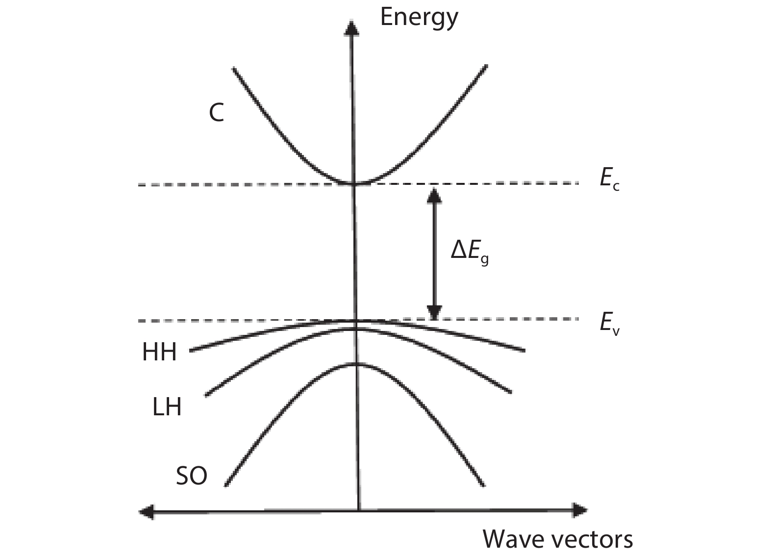
Fig. 1.
Schematic diagram showing the energy band states in the QW: conduction (C), heavy-hole (HH), light-hole (LH), and split-off (SO).
ARTICLES
A. Menani1, L. Dehimi1, 2, S. Dehimi3 and F. Pezzimenti4,
Corresponding author: F. Pezzimenti, Email: fortunato.pezzimenti@unirc.it
Abstract: The effects of the quantum well (QW) width, carrier density, and aluminium (Al) concentration in the barrier layers on the optical characteristics of a gallium nitride (GaN)-based QW laser diode are investigated by means of a careful modelling analysis in a wide range of temperatures. The device’s optical gain is calculated by using two different band energy models. The first is based on the simple band-to-band model that accounts for carrier transitions between the first levels of the conduction band and valence band, whereas the second assumes the perturbation theory (k.p model) for considering the valence intersubband transitions and the relative absorption losses in the QW. The results reveal that the optical gain increases with increasing the n-type doping density as well as the Al molar fraction of the AlxGa1–xN layers, which originate the GaN compressive-strained QW. In particular, a significant optical gain on the order of 5000 cm–1 is calculated for a QW width of 40 Å at room temperature. In addition, the laser threshold current density is of few tens of A/cm2 at low temperatures.
Keywords: laser diode, quantum well, optical gain, threshold current, temperature
| [1] |
Nakamura S, Fasol G. The blue laser diode. Berlin: Springer, 1997
|
| [2] |
Zory P S. Quantum well lasers. New York: Academic Press, 1993
|
| [3] |
Kieleck C, Eichhorn M, Hirth A, et al. High-efficiency 20–50 kHz mid-infrared orientation-patterned GaAs optical parametric oscillator pumped by a 2 μm holmium laser. Opt Lett, 2009, 34, 262 doi: 10.1364/OL.34.000262
|
| [4] |
Liu H C, Dudek R, Shen A, et al. High absorption quantum-well infrared photodetectors. Appl Phys Lett, 2001, 79, 4237 doi: 10.1063/1.1425066
|
| [5] |
Bouzid F, Pezzimenti F, Dehimi L, et al. Analytical modeling of dual-junction tandem solar cells based on an InGaP/GaAs heterojunction stacked on a Ge substrate. J Electron Mater, 2019, 48, 4107 doi: 10.1007/s11664-019-07180-z
|
| [6] |
Ustinov V M, Zhukov A E. GaAs-based long-wavelength lasers. Semicond Sci Technol, 2000, 15, R41 doi: 10.1088/0268-1242/15/8/201
|
| [7] |
Rogalski A. Infrared detectors: an overview. Infrared Phys Tech, 2002, 43, 187 doi: 10.1016/S1350-4495(02)00140-8
|
| [8] |
Justice J, Bower C, Meitl M, et al. Wafer-scale integration of group III–V lasers on silicon using transfer printing of epitaxial layers. Nat Photonics, 2012, 6, 610 doi: 10.1038/nphoton.2012.204
|
| [9] |
Bouzid F, Dehimi L, Pezzimenti F, et al. Numerical simulation study of a high efficient AlGaN-based ultraviolet photodetector. Superlattice Microstruct, 2018, 122, 57 doi: 10.1016/j.spmi.2018.08.022
|
| [10] |
Dehimi S, Dehimi L, Aissat A. Study and Simulation of a quantum well structure based ZnTe/Zn xCd1– xTe/ZnTe. Proc International Conference of Renewable Energy – CIER, 2014
|
| [11] |
Liu H, Wang T, Jiang Q, et al. Long-wavelength InAs/GaAs quantum-dot laser diode monolithically grown on Ge substrate. Nat Photonics, 2011, 5, 416 doi: 10.1038/nphoton.2011.120
|
| [12] |
Della Corte F G, De Martino G, Pezzimenti F, et al. Numerical simulation study of a low breakdown voltage 4H-SiC MOSFET for photovoltaic module-level applications. IEEE Trans Electron Devices, 2018, 65, 3352 doi: 10.1109/TED.2018.2848664
|
| [13] |
De Martino G, Pezzimenti F, Della Corte F G, et al. Design and numerical characterization of a low voltage power MOSFET in 4H-SiC for photovoltaic applications. Proc IEEE International Conference Ph. D. Research in Microelectronics and Electronics – PRIME, 2017
|
| [14] |
Yoshida H, Kuwabara M, Yamashita Y, et al. AlGaN-based laser diodes for the short-wavelength ultraviolet region. New J Phys, 2009, 11, 125013 doi: 10.1088/1367-2630/11/12/125013
|
| [15] |
Bouzid F, Dehimi L, Pezzimenti F. Performance analysis of a Pt/n-GaN Schottky barrier UV detector. J Electron Mater, 2017, 46, 6563 doi: 10.1007/s11664-017-5696-1
|
| [16] |
DenBaars S P, Feezell D, Kelchner K, et al. Development of gallium-nitride-based light-emitting diodes (LEDs) and laser diodes for energy-efficient lighting and displays. Acta Mater, 2013, 61, 945 doi: 10.1016/j.actamat.2012.10.042
|
| [17] |
Marouf Y, Dehimi L, Pezzimenti F. Simulation study for the current matching optimization in In0.48Ga0.52N/In0.74Ga0.26N dual junction solar cells. Superlattice Microstruct, 2019, 130, 377 doi: 10.1016/j.spmi.2019.05.004
|
| [18] |
Bencherif H, Dehimi L, Pezzimenti F, et al. Improving the efficiency of a-Si: H/c-Si thin heterojunction solar cells by using both antireflection coating engineering and diffraction grating. Optik, 2019, 182, 682 doi: 10.1016/j.ijleo.2019.01.032
|
| [19] |
Zeghdar K, Dehimi L, F Pezzimenti F, et al. Simulation and analysis of the current-voltage-temperature characteristics of Al/Ti/4H-SiC Schottky barrier diodes. Jpn J Appl Phys, 2019, 58, 014002 doi: 10.7567/1347-4065/aaf3ab
|
| [20] |
Fritah A, Dehimi L, Pezzimenti F, et al. Analysis of I–V–T characteristics of Au/n-InP Schottky barrier diodes with modeling of nanometer-sized patches at low temperature. J Electron Mater, 2019, 48, 3692 doi: 10.1007/s11664-019-07129-2
|
| [21] |
Farrell R M, Haeger D A, Hsu P S, et al. High-power blue-violet AlGaN-cladding-free m-plane InGaN/GaN laser diodes. Appl Phys Lett, 2011, 99, 171113 doi: 10.1063/1.3656970
|
| [22] |
Bouzid F, Pezzimenti F, Dehimi L, et al. Numerical simulations of the electrical transport characteristics of a Pt/n-GaN Schottky diode. Jpn J Appl Phys, 2017, 56, 094301 doi: 10.7567/JJAP.56.094301
|
| [23] |
Bencherif H, L Dehimi L, Pezzimenti F, et al. Analytical model for the light trapping effect on ZnO: Al/c-Si/SiGe/c-Si solar cells with an optimized design. Proc International Conference on Applied Smart Systems – ICASS, 2018
|
| [24] |
Marouf Y, Dehimi L, Bouzid F, et al. Theoretical design and performance of In xGa1– xN single junction solar cell. Optik, 2018, 163, 22 doi: 10.1016/j.ijleo.2018.02.106
|
| [25] |
Monroy E, Guillot F, Leconte S, et al. III-nitride nanostructures for infrared optoelectronics. Acta Phys Pol A, 2006, 110, 295 doi: 10.12693/APhysPolA.110.295
|
| [26] |
Rao S, Pangallo G, Pezzimenti F, et al. High-performance temperature sensor based on 4H-SiC Schottky diodes. IEEE Electron Device Lett, 2015, 36, 720 doi: 10.1109/LED.2015.2436213
|
| [27] |
De Martino G, Pezzimenti F, Della Corte F G. Interface trap effects in the design of a 4H-SiC MOSFET for low voltage applications. Proc International Semiconductor Conference – CAS, 2018
|
| [28] |
Bencherif H, Dehimi L, Pezzimenti F, et al. Temperature and SiO2/4H-SiC interface trap effects on the electrical characteristics of low breakdown voltage MOSFETs. Appl Phys A, 2019, 125, 294 doi: 10.1007/s00339-019-2606-9
|
| [29] |
Megherbi M L, Pezzimenti F, Dehimi L, et al. Analysis of different forward current-voltage behaviours of Al implanted 4H-SiC vertical p–i–n diodes. Solid-State Electron, 2015, 109, 12 doi: 10.1016/j.sse.2015.03.001
|
| [30] |
Bencherif H, Dehimi L, Pezzimenti F, et al. Multiobjective optimization of design of 4H-SiC power MOSFETs for specific applications. J Electron Mater, 2019, 48, 3871 doi: 10.1007/s11664-019-07142-5
|
| [31] |
Ikeda M, Mizuno T, Takeya M, et al. High-power GaN-based semiconductor lasers. Phys Status Solidi, 2004, 6, 1461 doi: 10.1002/pssc.200304086
|
| [32] |
Pezzimenti F, Bencherif H, Yousfi A, et al. Current–voltage analytical model and multiobjective optimization of design of a short channel gate-all-around-junctionless MOSFET. Solid-State Electron, 2019, 161, 107642 doi: 10.1016/j.sse.2019.107642
|
| [33] |
Asgari A, Dashti S. Optimization of optical gain in Al xGa1− xN/ GaN/Al xGa1− x N strained quantum well laser. Optik, 2012, 123, 1546 doi: 10.1016/j.ijleo.2011.09.014
|
| [34] |
Schubert E F, Kim J K. Solid-state light sources getting smart. Science, 2005, 308, 1274 doi: 10.1126/science.1108712
|
| [35] |
Ohtoshi T, Yamaguchi K, Nagaoka C, et al. A two dimensional device simulator of semiconductor lasers. Solid-State Electron, 1987, 30, 627 doi: 10.1016/0038-1101(87)90222-X
|
| [36] |
Chuang S L, Chang C S. k.p method for strained wurtzite semiconductors. Phys Rev B, 1996, 54, 2491 doi: 10.1103/PhysRevB.54.2491
|
| [37] |
Chuang S L. Optical gain of strained wurtzite GaN quantum-well lasers. IEEE J Quantum Electron, 1996, 32, 1791 doi: 10.1109/3.538786
|
| [38] |
Silvaco TCAD. Atlas user’s manual device simulation software. California: Silvaco Int., 2016
|
| [39] |
Bernardini F, Fiorentini V. Spontaneous versus piezoelectric polarization in III–V Nitrides: Conceptual aspects and practical consequences. Phys Status Solidi B, 1999, 216, 391 doi: 10.1002/(SICI)1521-3951(199911)216:1<391::AID-PSSB391>3.0.CO;2-K
|
| [40] |
Ambacher O, Majewski J, Miskys C, et al. Pyroelectric properties of Al(In)GaN/GaN heteroand quantum well structures. J Phys Condens Mat, 2002, 14, 3399 doi: 10.1088/0953-8984/14/13/302
|
| [41] |
Vurgaftman I, Meyer J R. Nitride semiconductor devices. New York: Wiley, 2007
|
| [42] |
Nepal N, Li J, Nakarmi M L, et al. Temperature and compositional dependence of AlGaN the energy band gap of alloys. Appl Phys Lett, 2005, 87, 242104 doi: 10.1063/1.2142333
|
| [43] |
Dakhlaoui H. Linear and nonlinear optical absorption coefficients and refractive index changes in GaN/Al xGa1– xN double quantum wells operating at 1.55 μm. J Appl Phys, 2015, 117, 1357051 doi: 10.1063/1.4916752
|
| [44] |
Dehimi S, Dehimi L, Asar T, et al. Modelling of a Cd1– x Zn xTe/ZnTe single quantum well for laser diodes. J Electron Mater, 2017, 46, 775 doi: 10.1007/s11664-016-4984-5
|
| [45] |
Casey H C, Panish M B. Heterostructure lasers. New York: Academic Press, 1978
|
| [46] |
Dehimi S, Dehimi L, Asar T, et al. Modeling and simulation of Zn xCd1– xTe/ZnTe quantum well structure for laser applications. Optik, 2017, 135, 153 doi: 10.1016/j.ijleo.2017.01.087
|
| [47] |
Dehimi S, Aissat A, Haddad D, et al. Optimization of optical gain in In xGa1– xSb/GaSb unstrained quantum well structures. Enrgy Proced, 2015, 74, 191 doi: 10.1016/j.egypro.2015.07.573
|
| [48] |
Aissat A, Nacer S, Ykhlef F, et al. Modeling of Ga1− xIn xAs1− y− zN ySb z/GaAs quantum well properties for near-infrared lasers. Mater Sci Semicond Proc, 2013, 16, 1936 doi: 10.1016/j.mssp.2013.07.021
|
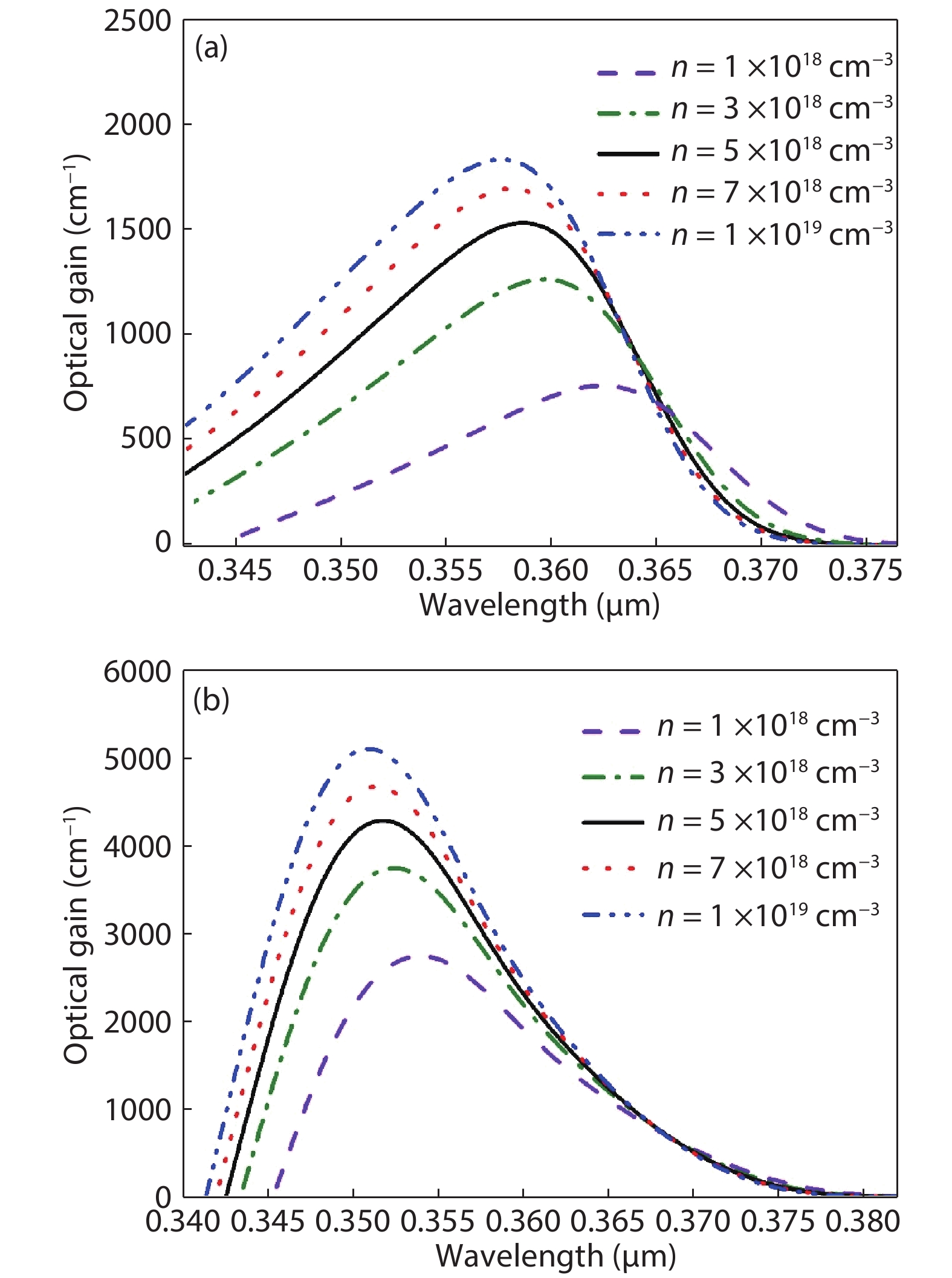
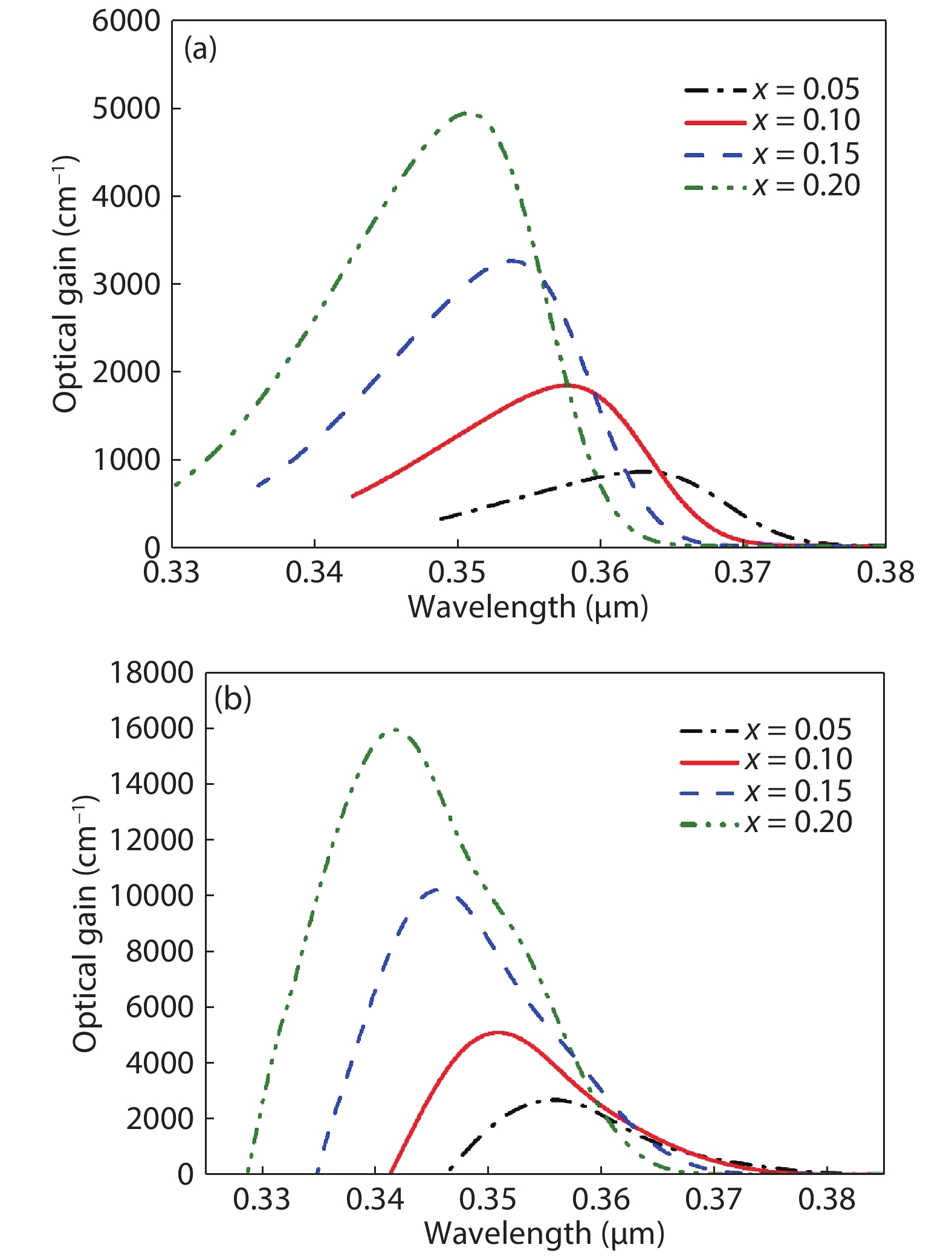
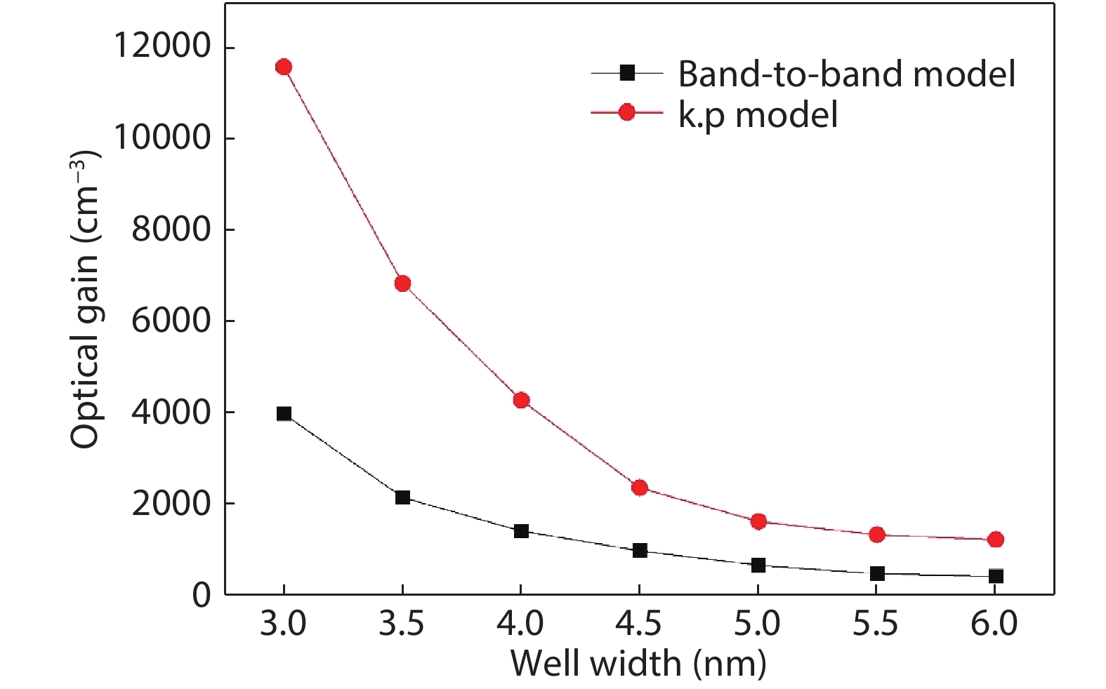
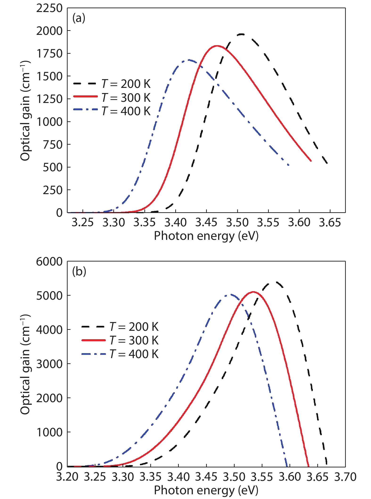
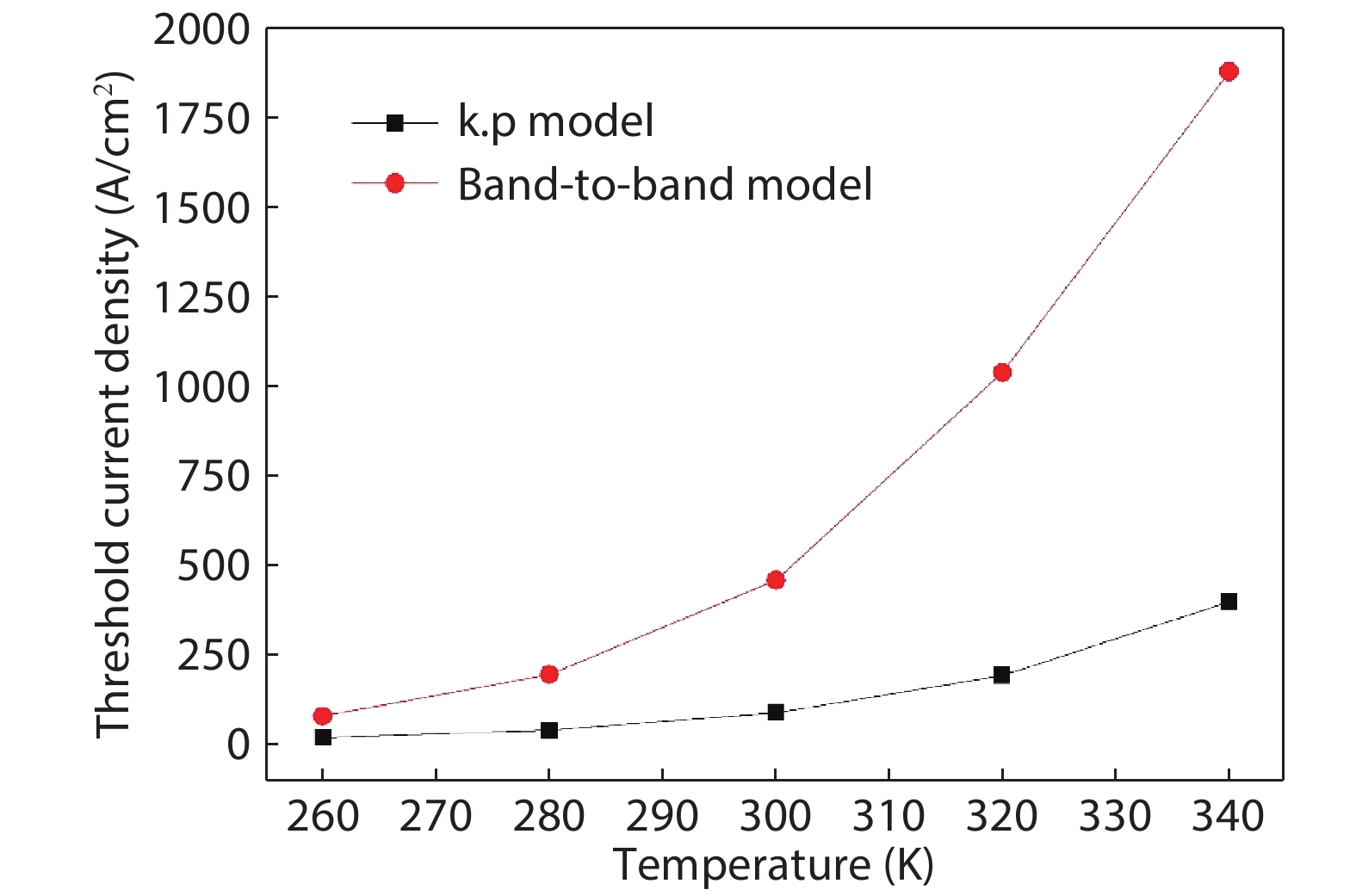
Table 1. Material parameters for wurtzite nitride binaries at T = 300 K.
| Parameter | GaN | AlN |
| Eg (eV) | 3.4 | 6.25 |
| α (meV/K) | 0.90 | 1.799 |
| β (K) | 830 | 1462 |
| mc/m0 | 0.20 | 0.33 |
| mv/m0 | 0.8 | 0.25 |
| a | 3.189 | 3.112 |
| c | 5.185 | 4.982 |
| Δ1 (eV) | 0.01 | –0.169 |
| Δ2 = Δ3 (eV) | 0.0056 | 0.0063 |
| A1 | –7.21 | –3.86 |
| A2 | –0.44 | –0.25 |
| A3 | 6.68 | 3.58 |
| A4 | –3.46 | –1.32 |
| A5 | –3.40 | –1.47 |
| A6 | –4.90 | –1.64 |
| D1 (eV) | –3.7 | –11.8 |
| D2 (eV) | 4.50 | 7.90 |
| D3 (eV) | 8.20 | 8.80 |
| D4 (eV) | –4.1 | –3.90 |
| C11 (GPa) | 390 | 396 |
| C12 (GPa) | 145 | 137 |
| C13 (GPa) | 106 | 108 |
| C33 (GPa) | 398 | 373 |
| dpz (pm/V) | –1.6 | –2.1 |
| Psp (C/m2) | –0.034 | –0.09 |
 DownLoad: CSV
| [1] |
Nakamura S, Fasol G. The blue laser diode. Berlin: Springer, 1997
|
| [2] |
Zory P S. Quantum well lasers. New York: Academic Press, 1993
|
| [3] |
Kieleck C, Eichhorn M, Hirth A, et al. High-efficiency 20–50 kHz mid-infrared orientation-patterned GaAs optical parametric oscillator pumped by a 2 μm holmium laser. Opt Lett, 2009, 34, 262 doi: 10.1364/OL.34.000262
|
| [4] |
Liu H C, Dudek R, Shen A, et al. High absorption quantum-well infrared photodetectors. Appl Phys Lett, 2001, 79, 4237 doi: 10.1063/1.1425066
|
| [5] |
Bouzid F, Pezzimenti F, Dehimi L, et al. Analytical modeling of dual-junction tandem solar cells based on an InGaP/GaAs heterojunction stacked on a Ge substrate. J Electron Mater, 2019, 48, 4107 doi: 10.1007/s11664-019-07180-z
|
| [6] |
Ustinov V M, Zhukov A E. GaAs-based long-wavelength lasers. Semicond Sci Technol, 2000, 15, R41 doi: 10.1088/0268-1242/15/8/201
|
| [7] |
Rogalski A. Infrared detectors: an overview. Infrared Phys Tech, 2002, 43, 187 doi: 10.1016/S1350-4495(02)00140-8
|
| [8] |
Justice J, Bower C, Meitl M, et al. Wafer-scale integration of group III–V lasers on silicon using transfer printing of epitaxial layers. Nat Photonics, 2012, 6, 610 doi: 10.1038/nphoton.2012.204
|
| [9] |
Bouzid F, Dehimi L, Pezzimenti F, et al. Numerical simulation study of a high efficient AlGaN-based ultraviolet photodetector. Superlattice Microstruct, 2018, 122, 57 doi: 10.1016/j.spmi.2018.08.022
|
| [10] |
Dehimi S, Dehimi L, Aissat A. Study and Simulation of a quantum well structure based ZnTe/Zn xCd1– xTe/ZnTe. Proc International Conference of Renewable Energy – CIER, 2014
|
| [11] |
Liu H, Wang T, Jiang Q, et al. Long-wavelength InAs/GaAs quantum-dot laser diode monolithically grown on Ge substrate. Nat Photonics, 2011, 5, 416 doi: 10.1038/nphoton.2011.120
|
| [12] |
Della Corte F G, De Martino G, Pezzimenti F, et al. Numerical simulation study of a low breakdown voltage 4H-SiC MOSFET for photovoltaic module-level applications. IEEE Trans Electron Devices, 2018, 65, 3352 doi: 10.1109/TED.2018.2848664
|
| [13] |
De Martino G, Pezzimenti F, Della Corte F G, et al. Design and numerical characterization of a low voltage power MOSFET in 4H-SiC for photovoltaic applications. Proc IEEE International Conference Ph. D. Research in Microelectronics and Electronics – PRIME, 2017
|
| [14] |
Yoshida H, Kuwabara M, Yamashita Y, et al. AlGaN-based laser diodes for the short-wavelength ultraviolet region. New J Phys, 2009, 11, 125013 doi: 10.1088/1367-2630/11/12/125013
|
| [15] |
Bouzid F, Dehimi L, Pezzimenti F. Performance analysis of a Pt/n-GaN Schottky barrier UV detector. J Electron Mater, 2017, 46, 6563 doi: 10.1007/s11664-017-5696-1
|
| [16] |
DenBaars S P, Feezell D, Kelchner K, et al. Development of gallium-nitride-based light-emitting diodes (LEDs) and laser diodes for energy-efficient lighting and displays. Acta Mater, 2013, 61, 945 doi: 10.1016/j.actamat.2012.10.042
|
| [17] |
Marouf Y, Dehimi L, Pezzimenti F. Simulation study for the current matching optimization in In0.48Ga0.52N/In0.74Ga0.26N dual junction solar cells. Superlattice Microstruct, 2019, 130, 377 doi: 10.1016/j.spmi.2019.05.004
|
| [18] |
Bencherif H, Dehimi L, Pezzimenti F, et al. Improving the efficiency of a-Si: H/c-Si thin heterojunction solar cells by using both antireflection coating engineering and diffraction grating. Optik, 2019, 182, 682 doi: 10.1016/j.ijleo.2019.01.032
|
| [19] |
Zeghdar K, Dehimi L, F Pezzimenti F, et al. Simulation and analysis of the current-voltage-temperature characteristics of Al/Ti/4H-SiC Schottky barrier diodes. Jpn J Appl Phys, 2019, 58, 014002 doi: 10.7567/1347-4065/aaf3ab
|
| [20] |
Fritah A, Dehimi L, Pezzimenti F, et al. Analysis of I–V–T characteristics of Au/n-InP Schottky barrier diodes with modeling of nanometer-sized patches at low temperature. J Electron Mater, 2019, 48, 3692 doi: 10.1007/s11664-019-07129-2
|
| [21] |
Farrell R M, Haeger D A, Hsu P S, et al. High-power blue-violet AlGaN-cladding-free m-plane InGaN/GaN laser diodes. Appl Phys Lett, 2011, 99, 171113 doi: 10.1063/1.3656970
|
| [22] |
Bouzid F, Pezzimenti F, Dehimi L, et al. Numerical simulations of the electrical transport characteristics of a Pt/n-GaN Schottky diode. Jpn J Appl Phys, 2017, 56, 094301 doi: 10.7567/JJAP.56.094301
|
| [23] |
Bencherif H, L Dehimi L, Pezzimenti F, et al. Analytical model for the light trapping effect on ZnO: Al/c-Si/SiGe/c-Si solar cells with an optimized design. Proc International Conference on Applied Smart Systems – ICASS, 2018
|
| [24] |
Marouf Y, Dehimi L, Bouzid F, et al. Theoretical design and performance of In xGa1– xN single junction solar cell. Optik, 2018, 163, 22 doi: 10.1016/j.ijleo.2018.02.106
|
| [25] |
Monroy E, Guillot F, Leconte S, et al. III-nitride nanostructures for infrared optoelectronics. Acta Phys Pol A, 2006, 110, 295 doi: 10.12693/APhysPolA.110.295
|
| [26] |
Rao S, Pangallo G, Pezzimenti F, et al. High-performance temperature sensor based on 4H-SiC Schottky diodes. IEEE Electron Device Lett, 2015, 36, 720 doi: 10.1109/LED.2015.2436213
|
| [27] |
De Martino G, Pezzimenti F, Della Corte F G. Interface trap effects in the design of a 4H-SiC MOSFET for low voltage applications. Proc International Semiconductor Conference – CAS, 2018
|
| [28] |
Bencherif H, Dehimi L, Pezzimenti F, et al. Temperature and SiO2/4H-SiC interface trap effects on the electrical characteristics of low breakdown voltage MOSFETs. Appl Phys A, 2019, 125, 294 doi: 10.1007/s00339-019-2606-9
|
| [29] |
Megherbi M L, Pezzimenti F, Dehimi L, et al. Analysis of different forward current-voltage behaviours of Al implanted 4H-SiC vertical p–i–n diodes. Solid-State Electron, 2015, 109, 12 doi: 10.1016/j.sse.2015.03.001
|
| [30] |
Bencherif H, Dehimi L, Pezzimenti F, et al. Multiobjective optimization of design of 4H-SiC power MOSFETs for specific applications. J Electron Mater, 2019, 48, 3871 doi: 10.1007/s11664-019-07142-5
|
| [31] |
Ikeda M, Mizuno T, Takeya M, et al. High-power GaN-based semiconductor lasers. Phys Status Solidi, 2004, 6, 1461 doi: 10.1002/pssc.200304086
|
| [32] |
Pezzimenti F, Bencherif H, Yousfi A, et al. Current–voltage analytical model and multiobjective optimization of design of a short channel gate-all-around-junctionless MOSFET. Solid-State Electron, 2019, 161, 107642 doi: 10.1016/j.sse.2019.107642
|
| [33] |
Asgari A, Dashti S. Optimization of optical gain in Al xGa1− xN/ GaN/Al xGa1− x N strained quantum well laser. Optik, 2012, 123, 1546 doi: 10.1016/j.ijleo.2011.09.014
|
| [34] |
Schubert E F, Kim J K. Solid-state light sources getting smart. Science, 2005, 308, 1274 doi: 10.1126/science.1108712
|
| [35] |
Ohtoshi T, Yamaguchi K, Nagaoka C, et al. A two dimensional device simulator of semiconductor lasers. Solid-State Electron, 1987, 30, 627 doi: 10.1016/0038-1101(87)90222-X
|
| [36] |
Chuang S L, Chang C S. k.p method for strained wurtzite semiconductors. Phys Rev B, 1996, 54, 2491 doi: 10.1103/PhysRevB.54.2491
|
| [37] |
Chuang S L. Optical gain of strained wurtzite GaN quantum-well lasers. IEEE J Quantum Electron, 1996, 32, 1791 doi: 10.1109/3.538786
|
| [38] |
Silvaco TCAD. Atlas user’s manual device simulation software. California: Silvaco Int., 2016
|
| [39] |
Bernardini F, Fiorentini V. Spontaneous versus piezoelectric polarization in III–V Nitrides: Conceptual aspects and practical consequences. Phys Status Solidi B, 1999, 216, 391 doi: 10.1002/(SICI)1521-3951(199911)216:1<391::AID-PSSB391>3.0.CO;2-K
|
| [40] |
Ambacher O, Majewski J, Miskys C, et al. Pyroelectric properties of Al(In)GaN/GaN heteroand quantum well structures. J Phys Condens Mat, 2002, 14, 3399 doi: 10.1088/0953-8984/14/13/302
|
| [41] |
Vurgaftman I, Meyer J R. Nitride semiconductor devices. New York: Wiley, 2007
|
| [42] |
Nepal N, Li J, Nakarmi M L, et al. Temperature and compositional dependence of AlGaN the energy band gap of alloys. Appl Phys Lett, 2005, 87, 242104 doi: 10.1063/1.2142333
|
| [43] |
Dakhlaoui H. Linear and nonlinear optical absorption coefficients and refractive index changes in GaN/Al xGa1– xN double quantum wells operating at 1.55 μm. J Appl Phys, 2015, 117, 1357051 doi: 10.1063/1.4916752
|
| [44] |
Dehimi S, Dehimi L, Asar T, et al. Modelling of a Cd1– x Zn xTe/ZnTe single quantum well for laser diodes. J Electron Mater, 2017, 46, 775 doi: 10.1007/s11664-016-4984-5
|
| [45] |
Casey H C, Panish M B. Heterostructure lasers. New York: Academic Press, 1978
|
| [46] |
Dehimi S, Dehimi L, Asar T, et al. Modeling and simulation of Zn xCd1– xTe/ZnTe quantum well structure for laser applications. Optik, 2017, 135, 153 doi: 10.1016/j.ijleo.2017.01.087
|
| [47] |
Dehimi S, Aissat A, Haddad D, et al. Optimization of optical gain in In xGa1– xSb/GaSb unstrained quantum well structures. Enrgy Proced, 2015, 74, 191 doi: 10.1016/j.egypro.2015.07.573
|
| [48] |
Aissat A, Nacer S, Ykhlef F, et al. Modeling of Ga1− xIn xAs1− y− zN ySb z/GaAs quantum well properties for near-infrared lasers. Mater Sci Semicond Proc, 2013, 16, 1936 doi: 10.1016/j.mssp.2013.07.021
|


Article views: 5889 Times PDF downloads: 188 Times Cited by: 0 Times
Received: 19 September 2019 Revised: 05 December 2019 Online: Accepted Manuscript: 20 January 2020Uncorrected proof: 13 February 2020Published: 01 June 2020
| Citation: |
A. Menani, L. Dehimi, S. Dehimi, F. Pezzimenti. Modelling and optical response of a compressive-strained AlGaN/GaN quantum well laser diode[J]. Journal of Semiconductors, 2020, 41(6): 062301. doi: 10.1088/1674-4926/41/6/062301
****
A Menani, L Dehimi, S Dehimi, F Pezzimenti, Modelling and optical response of a compressive-strained AlGaN/GaN quantum well laser diode[J]. J. Semicond., 2020, 41(6): 062301. doi: 10.1088/1674-4926/41/6/062301.

|
| [1] |
Nakamura S, Fasol G. The blue laser diode. Berlin: Springer, 1997
|
| [2] |
Zory P S. Quantum well lasers. New York: Academic Press, 1993
|
| [3] |
Kieleck C, Eichhorn M, Hirth A, et al. High-efficiency 20–50 kHz mid-infrared orientation-patterned GaAs optical parametric oscillator pumped by a 2 μm holmium laser. Opt Lett, 2009, 34, 262 doi: 10.1364/OL.34.000262
|
| [4] |
Liu H C, Dudek R, Shen A, et al. High absorption quantum-well infrared photodetectors. Appl Phys Lett, 2001, 79, 4237 doi: 10.1063/1.1425066
|
| [5] |
Bouzid F, Pezzimenti F, Dehimi L, et al. Analytical modeling of dual-junction tandem solar cells based on an InGaP/GaAs heterojunction stacked on a Ge substrate. J Electron Mater, 2019, 48, 4107 doi: 10.1007/s11664-019-07180-z
|
| [6] |
Ustinov V M, Zhukov A E. GaAs-based long-wavelength lasers. Semicond Sci Technol, 2000, 15, R41 doi: 10.1088/0268-1242/15/8/201
|
| [7] |
Rogalski A. Infrared detectors: an overview. Infrared Phys Tech, 2002, 43, 187 doi: 10.1016/S1350-4495(02)00140-8
|
| [8] |
Justice J, Bower C, Meitl M, et al. Wafer-scale integration of group III–V lasers on silicon using transfer printing of epitaxial layers. Nat Photonics, 2012, 6, 610 doi: 10.1038/nphoton.2012.204
|
| [9] |
Bouzid F, Dehimi L, Pezzimenti F, et al. Numerical simulation study of a high efficient AlGaN-based ultraviolet photodetector. Superlattice Microstruct, 2018, 122, 57 doi: 10.1016/j.spmi.2018.08.022
|
| [10] |
Dehimi S, Dehimi L, Aissat A. Study and Simulation of a quantum well structure based ZnTe/Zn xCd1– xTe/ZnTe. Proc International Conference of Renewable Energy – CIER, 2014
|
| [11] |
Liu H, Wang T, Jiang Q, et al. Long-wavelength InAs/GaAs quantum-dot laser diode monolithically grown on Ge substrate. Nat Photonics, 2011, 5, 416 doi: 10.1038/nphoton.2011.120
|
| [12] |
Della Corte F G, De Martino G, Pezzimenti F, et al. Numerical simulation study of a low breakdown voltage 4H-SiC MOSFET for photovoltaic module-level applications. IEEE Trans Electron Devices, 2018, 65, 3352 doi: 10.1109/TED.2018.2848664
|
| [13] |
De Martino G, Pezzimenti F, Della Corte F G, et al. Design and numerical characterization of a low voltage power MOSFET in 4H-SiC for photovoltaic applications. Proc IEEE International Conference Ph. D. Research in Microelectronics and Electronics – PRIME, 2017
|
| [14] |
Yoshida H, Kuwabara M, Yamashita Y, et al. AlGaN-based laser diodes for the short-wavelength ultraviolet region. New J Phys, 2009, 11, 125013 doi: 10.1088/1367-2630/11/12/125013
|
| [15] |
Bouzid F, Dehimi L, Pezzimenti F. Performance analysis of a Pt/n-GaN Schottky barrier UV detector. J Electron Mater, 2017, 46, 6563 doi: 10.1007/s11664-017-5696-1
|
| [16] |
DenBaars S P, Feezell D, Kelchner K, et al. Development of gallium-nitride-based light-emitting diodes (LEDs) and laser diodes for energy-efficient lighting and displays. Acta Mater, 2013, 61, 945 doi: 10.1016/j.actamat.2012.10.042
|
| [17] |
Marouf Y, Dehimi L, Pezzimenti F. Simulation study for the current matching optimization in In0.48Ga0.52N/In0.74Ga0.26N dual junction solar cells. Superlattice Microstruct, 2019, 130, 377 doi: 10.1016/j.spmi.2019.05.004
|
| [18] |
Bencherif H, Dehimi L, Pezzimenti F, et al. Improving the efficiency of a-Si: H/c-Si thin heterojunction solar cells by using both antireflection coating engineering and diffraction grating. Optik, 2019, 182, 682 doi: 10.1016/j.ijleo.2019.01.032
|
| [19] |
Zeghdar K, Dehimi L, F Pezzimenti F, et al. Simulation and analysis of the current-voltage-temperature characteristics of Al/Ti/4H-SiC Schottky barrier diodes. Jpn J Appl Phys, 2019, 58, 014002 doi: 10.7567/1347-4065/aaf3ab
|
| [20] |
Fritah A, Dehimi L, Pezzimenti F, et al. Analysis of I–V–T characteristics of Au/n-InP Schottky barrier diodes with modeling of nanometer-sized patches at low temperature. J Electron Mater, 2019, 48, 3692 doi: 10.1007/s11664-019-07129-2
|
| [21] |
Farrell R M, Haeger D A, Hsu P S, et al. High-power blue-violet AlGaN-cladding-free m-plane InGaN/GaN laser diodes. Appl Phys Lett, 2011, 99, 171113 doi: 10.1063/1.3656970
|
| [22] |
Bouzid F, Pezzimenti F, Dehimi L, et al. Numerical simulations of the electrical transport characteristics of a Pt/n-GaN Schottky diode. Jpn J Appl Phys, 2017, 56, 094301 doi: 10.7567/JJAP.56.094301
|
| [23] |
Bencherif H, L Dehimi L, Pezzimenti F, et al. Analytical model for the light trapping effect on ZnO: Al/c-Si/SiGe/c-Si solar cells with an optimized design. Proc International Conference on Applied Smart Systems – ICASS, 2018
|
| [24] |
Marouf Y, Dehimi L, Bouzid F, et al. Theoretical design and performance of In xGa1– xN single junction solar cell. Optik, 2018, 163, 22 doi: 10.1016/j.ijleo.2018.02.106
|
| [25] |
Monroy E, Guillot F, Leconte S, et al. III-nitride nanostructures for infrared optoelectronics. Acta Phys Pol A, 2006, 110, 295 doi: 10.12693/APhysPolA.110.295
|
| [26] |
Rao S, Pangallo G, Pezzimenti F, et al. High-performance temperature sensor based on 4H-SiC Schottky diodes. IEEE Electron Device Lett, 2015, 36, 720 doi: 10.1109/LED.2015.2436213
|
| [27] |
De Martino G, Pezzimenti F, Della Corte F G. Interface trap effects in the design of a 4H-SiC MOSFET for low voltage applications. Proc International Semiconductor Conference – CAS, 2018
|
| [28] |
Bencherif H, Dehimi L, Pezzimenti F, et al. Temperature and SiO2/4H-SiC interface trap effects on the electrical characteristics of low breakdown voltage MOSFETs. Appl Phys A, 2019, 125, 294 doi: 10.1007/s00339-019-2606-9
|
| [29] |
Megherbi M L, Pezzimenti F, Dehimi L, et al. Analysis of different forward current-voltage behaviours of Al implanted 4H-SiC vertical p–i–n diodes. Solid-State Electron, 2015, 109, 12 doi: 10.1016/j.sse.2015.03.001
|
| [30] |
Bencherif H, Dehimi L, Pezzimenti F, et al. Multiobjective optimization of design of 4H-SiC power MOSFETs for specific applications. J Electron Mater, 2019, 48, 3871 doi: 10.1007/s11664-019-07142-5
|
| [31] |
Ikeda M, Mizuno T, Takeya M, et al. High-power GaN-based semiconductor lasers. Phys Status Solidi, 2004, 6, 1461 doi: 10.1002/pssc.200304086
|
| [32] |
Pezzimenti F, Bencherif H, Yousfi A, et al. Current–voltage analytical model and multiobjective optimization of design of a short channel gate-all-around-junctionless MOSFET. Solid-State Electron, 2019, 161, 107642 doi: 10.1016/j.sse.2019.107642
|
| [33] |
Asgari A, Dashti S. Optimization of optical gain in Al xGa1− xN/ GaN/Al xGa1− x N strained quantum well laser. Optik, 2012, 123, 1546 doi: 10.1016/j.ijleo.2011.09.014
|
| [34] |
Schubert E F, Kim J K. Solid-state light sources getting smart. Science, 2005, 308, 1274 doi: 10.1126/science.1108712
|
| [35] |
Ohtoshi T, Yamaguchi K, Nagaoka C, et al. A two dimensional device simulator of semiconductor lasers. Solid-State Electron, 1987, 30, 627 doi: 10.1016/0038-1101(87)90222-X
|
| [36] |
Chuang S L, Chang C S. k.p method for strained wurtzite semiconductors. Phys Rev B, 1996, 54, 2491 doi: 10.1103/PhysRevB.54.2491
|
| [37] |
Chuang S L. Optical gain of strained wurtzite GaN quantum-well lasers. IEEE J Quantum Electron, 1996, 32, 1791 doi: 10.1109/3.538786
|
| [38] |
Silvaco TCAD. Atlas user’s manual device simulation software. California: Silvaco Int., 2016
|
| [39] |
Bernardini F, Fiorentini V. Spontaneous versus piezoelectric polarization in III–V Nitrides: Conceptual aspects and practical consequences. Phys Status Solidi B, 1999, 216, 391 doi: 10.1002/(SICI)1521-3951(199911)216:1<391::AID-PSSB391>3.0.CO;2-K
|
| [40] |
Ambacher O, Majewski J, Miskys C, et al. Pyroelectric properties of Al(In)GaN/GaN heteroand quantum well structures. J Phys Condens Mat, 2002, 14, 3399 doi: 10.1088/0953-8984/14/13/302
|
| [41] |
Vurgaftman I, Meyer J R. Nitride semiconductor devices. New York: Wiley, 2007
|
| [42] |
Nepal N, Li J, Nakarmi M L, et al. Temperature and compositional dependence of AlGaN the energy band gap of alloys. Appl Phys Lett, 2005, 87, 242104 doi: 10.1063/1.2142333
|
| [43] |
Dakhlaoui H. Linear and nonlinear optical absorption coefficients and refractive index changes in GaN/Al xGa1– xN double quantum wells operating at 1.55 μm. J Appl Phys, 2015, 117, 1357051 doi: 10.1063/1.4916752
|
| [44] |
Dehimi S, Dehimi L, Asar T, et al. Modelling of a Cd1– x Zn xTe/ZnTe single quantum well for laser diodes. J Electron Mater, 2017, 46, 775 doi: 10.1007/s11664-016-4984-5
|
| [45] |
Casey H C, Panish M B. Heterostructure lasers. New York: Academic Press, 1978
|
| [46] |
Dehimi S, Dehimi L, Asar T, et al. Modeling and simulation of Zn xCd1– xTe/ZnTe quantum well structure for laser applications. Optik, 2017, 135, 153 doi: 10.1016/j.ijleo.2017.01.087
|
| [47] |
Dehimi S, Aissat A, Haddad D, et al. Optimization of optical gain in In xGa1– xSb/GaSb unstrained quantum well structures. Enrgy Proced, 2015, 74, 191 doi: 10.1016/j.egypro.2015.07.573
|
| [48] |
Aissat A, Nacer S, Ykhlef F, et al. Modeling of Ga1− xIn xAs1− y− zN ySb z/GaAs quantum well properties for near-infrared lasers. Mater Sci Semicond Proc, 2013, 16, 1936 doi: 10.1016/j.mssp.2013.07.021
|

 WeChat ID
Journal of Semiconductors © 2017 All Rights Reserved 京ICP备05085259号-2


