J. Semicond. > 2020, Volume 41 > Issue 6 > 062302

ARTICLES

Strain-induced the dark current characteristics in InAs/GaSb type-II superlattice for mid-wave detector

H. J. Lee1, 2, S. Y. Ko1, Y. H. Kim1 and J. Nah2,

+ Author Affiliations

 Corresponding author: J. Nah, jnah@cnu.ac.kr

DOI: 10.1088/1674-4926/41/6/062302

PDF

Turn off MathJax

Abstract: Type-II superlattice (T2SL) materials are the key element for infrared (IR) detectors. However, it is well known that the characteristics of the detectors with the T2SL layer are greatly affected by the strain developed during the growth process, which determines the performance of IR detectors. Therefore, great efforts have been made to properly control the strain effect and develop relevant analysis methods to evaluate the strain-induced dark current characteristics. In this work, we report the strain-induced dark current characteristics in InAs/GaSb T2SL MWIR photodetector. The overall strain of InAs/GaSb T2SL layer was analyzed by both high-resolution X-ray diffraction (HRXRD) and the dark current measured from the absorber layer at the elevated temperatures (≥ 110 K), where the major leakage current component is originated from the reduced minority carrier lifetime in the absorber layer. Our findings indicate that minority carrier lifetime increases as the tensile strain on the InAs/GaSb T2SL is more compensated by the compressive strain through ‘InSb-like’ interface, which reduces the dark current density of the device. Specifically, tensile strain compensated devices exhibited the dark current density of less than 2 ×10⁻⁵ A/cm2 at 120 K, which is more than one order of magnitude lower value compared to that of the device without tensile strain relaxation.

Key words: mid-wave detectorInAs/GaSb type II super latticedark current


[1]
Rogalski A. Recent process in infrared detector technologies. Infrared Phys Technol, 2011, 54(3), 136 doi: 10.1016/j.infrared.2010.12.003
[2]
Rogalski A, Martyniuk P, Kopytko M. Challenges of small pixel infrared detectors: A review. Rep Prog Phys, 2016, 79(046501), 1 doi: 10.1088/0034-4885/79/4/046501
[3]
Rogalski A. Next decade in infrared detectors. Proc SPIE, 2017, 10433, 104330L
[4]
Rhiger D, Kvaas R, Harris S, et al. Progress with type-II superlattice IR detector arrays. Proc SPIE, 2007, 6542, 654202 doi: 10.1117/12.716101
[5]
Herres N, Fuchs F, Schmitz J, et al. Effect of interfacial bonding on the structural and vibrational properties of InAs/GaSb superlattices. Phys Rev B, 1996, 53(23), 15688 doi: 10.1103/PhysRevB.53.15688
[6]
Steinshnider J, Weimer M, Kaspi R, et al. Visualizing interfacial structure at non-common-atom heterojunctions with cross-sectional scanning tunneling microscopy. Phys Rev Lett, 2000, 85(14), 2953 doi: 10.1103/PhysRevLett.85.2953
[7]
Lyapin S, Klipstein P, Mason N, et al. Raman selection rules for the observation of interface modes in InAs/GaSb superlattices. Phy Rev Lett, 1995, 74(16), 3285 doi: 10.1103/PhysRevLett.74.3285
[8]
Plis E, Annamalai S, Posani K, et al. Midwave infrared type-II InAs/GaSb superlattice detectors with mixed interfaces. J Appl Phys, 2006, 100(1), 014510 doi: 10.1063/1.2214222
[9]
Rodriguez J, Christol P, Cerutti L, et al. MBE growth and characterization of type-II InAs/GaSb superlattices for mid-infrared detection. J Cryst Growth, 2005, 274(1–2), 6 doi: 10.1016/j.jcrysgro.2004.09.088
[10]
Liu G, Fruhberger B, Schuller I, et al. Quantitative structural characterization of InAs/GaSb superlatties. J Appl Phys, 2006, 100(6), 063536 doi: 10.1063/1.2353732
[11]
Zuo D, Qiao P, Wasserman D, et al. Direct observation of minority carrier lifetime improvement in InAs/GaSb type-II superlattice photodiodes via interfacial layer control. Appl Phys Lett, 2013, 102(14), 141107 doi: 10.1063/1.4801764
[12]
Zhang Y, Ma W, Huang J, et al. Long wavelength infrared InAs/GaSb superlattice photodetectors with InSb-like and mixed interfaces. IEEE J Quantum Electron, 2011, 47(12), 1475 doi: 10.1109/JQE.2011.2168947
[13]
Song Y, Wang S, Asplund C, et al. Growth optimization, strain compensation and structure design of InAs/GaSb type-II superlattices for mid-infrared imaging. Cryst Struct Theory Appl, 2013, 02(02), 46 doi: 10.4236/csta.2013.22007
[14]
Kim H, Meng Y, Rouviére J, et al. Atomic resolution mapping of interfacial intermixing and segration in InAs/GaSb superlattices: A correlative study. J Appl Phys, 2013, 113(10), 103511 doi: 10.1063/1.4794193
[15]
Mahalingam K, Haugan H, Brown G, et al. Strain analysis of compositionally tailored interfaces in InAs/GaSb superlattices. Appl Phys Lett, 2013, 103(21), 211605 doi: 10.1063/1.4833536
[16]
Ashuach Y, Lakin E, Saguy C, et al. Atomic intermixing and interface roughness in short-period InAs/GaSb superlattices for infrared photodetectors. J Appl Phys, 2014, 116(12), 124315 doi: 10.1063/1.4896834
[17]
Meng Y, Kim H, Rouviére J, et al. Digital model for X-ray diffraction with application to composition and strain determination in strained InAs/GaSb superlattices. J Appl Phys, 2014, 116(1), 013513 doi: 10.1063/1.4887078
[18]
Sun Y, Wang G, Xiang W, et al. 320 × 256 high operating temperature mid-infrared focal plane arrays based on type-II InAs/GaSb superlattice. Superlattices Microstruct, 2017, 111, 783 doi: 10.1016/j.spmi.2017.07.037
[19]
Höglund S, Naureen R, Ivanov M, et al. Type II superlattices: HOT MWIR production and development at IRnova. Proc SPIE, 2019, 11002, 110020U
Fig. 1.  (Color online) (a) The schematic of the InAs/GaSb T2SL MWIR epi. structure with nBn structure. (b) TEM image of the absorber layer with InAs/GaSb 10/10 MLs. The inset on right corner shows a magnitude view taken in HAADF mode. (c) The schematics of the InAs/GaSb T2SL nBn device fabrication process. Fist, each pixel is isolated by etching the top contact layer and the barrier using C6H8O7/H3PO4/H2O2/H2O solution. After wet-treatment to remove a native oxide at the surface, SiO2 passivation layer is deposited using PECVD. Finally, the contact metal is evaporated for both pixels and common electrode.

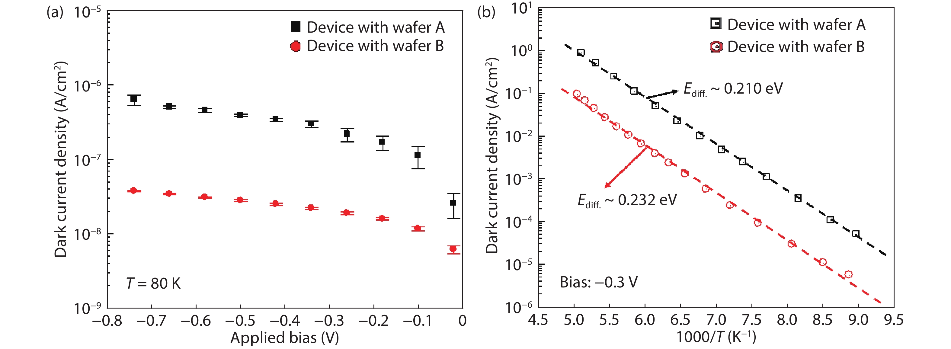
Fig. 2.  (Color online) (a) The dark current density versus applied bias at 80 K. The identical fabrication process is used for device fabrication on the wafers A and B. Approximately, one order of magnitude higher dark current density is observed from the devices on the wafer A. (b) Arrhenius plots of the devices fabricated on the wafers A and B. Both devices demonstrate diffusion-limited current but different activation energies. The plot indicates that the minority carrier lifetime in the absorber layer of the devices on the wafer B is longer than those on the wafer A.

Fig. 3.  (Color online) Spectral response of the devices fabricated on the wafers A and B. The cut-off wavelength of the devices on the wafer B is shorter than those on the wafer A. The result is consistent with the results in Fig. 2, exhibiting difference activation energies.

Fig. 4.  High-resolution X-ray omega-2theta scan data of InAs/GaSb T2SL and Al0.2Ga0.8Sb around GaSb (004) peak.

Table 1.   Analysis of HRXRD patterns.

No. wafer Strain type Periodicity (Å) Mismatch (ppm)
A Tensile 59.18 788.6
B Tensile 59.06 67.37
DownLoad: CSV
[1]
Rogalski A. Recent process in infrared detector technologies. Infrared Phys Technol, 2011, 54(3), 136 doi: 10.1016/j.infrared.2010.12.003
[2]
Rogalski A, Martyniuk P, Kopytko M. Challenges of small pixel infrared detectors: A review. Rep Prog Phys, 2016, 79(046501), 1 doi: 10.1088/0034-4885/79/4/046501
[3]
Rogalski A. Next decade in infrared detectors. Proc SPIE, 2017, 10433, 104330L
[4]
Rhiger D, Kvaas R, Harris S, et al. Progress with type-II superlattice IR detector arrays. Proc SPIE, 2007, 6542, 654202 doi: 10.1117/12.716101
[5]
Herres N, Fuchs F, Schmitz J, et al. Effect of interfacial bonding on the structural and vibrational properties of InAs/GaSb superlattices. Phys Rev B, 1996, 53(23), 15688 doi: 10.1103/PhysRevB.53.15688
[6]
Steinshnider J, Weimer M, Kaspi R, et al. Visualizing interfacial structure at non-common-atom heterojunctions with cross-sectional scanning tunneling microscopy. Phys Rev Lett, 2000, 85(14), 2953 doi: 10.1103/PhysRevLett.85.2953
[7]
Lyapin S, Klipstein P, Mason N, et al. Raman selection rules for the observation of interface modes in InAs/GaSb superlattices. Phy Rev Lett, 1995, 74(16), 3285 doi: 10.1103/PhysRevLett.74.3285
[8]
Plis E, Annamalai S, Posani K, et al. Midwave infrared type-II InAs/GaSb superlattice detectors with mixed interfaces. J Appl Phys, 2006, 100(1), 014510 doi: 10.1063/1.2214222
[9]
Rodriguez J, Christol P, Cerutti L, et al. MBE growth and characterization of type-II InAs/GaSb superlattices for mid-infrared detection. J Cryst Growth, 2005, 274(1–2), 6 doi: 10.1016/j.jcrysgro.2004.09.088
[10]
Liu G, Fruhberger B, Schuller I, et al. Quantitative structural characterization of InAs/GaSb superlatties. J Appl Phys, 2006, 100(6), 063536 doi: 10.1063/1.2353732
[11]
Zuo D, Qiao P, Wasserman D, et al. Direct observation of minority carrier lifetime improvement in InAs/GaSb type-II superlattice photodiodes via interfacial layer control. Appl Phys Lett, 2013, 102(14), 141107 doi: 10.1063/1.4801764
[12]
Zhang Y, Ma W, Huang J, et al. Long wavelength infrared InAs/GaSb superlattice photodetectors with InSb-like and mixed interfaces. IEEE J Quantum Electron, 2011, 47(12), 1475 doi: 10.1109/JQE.2011.2168947
[13]
Song Y, Wang S, Asplund C, et al. Growth optimization, strain compensation and structure design of InAs/GaSb type-II superlattices for mid-infrared imaging. Cryst Struct Theory Appl, 2013, 02(02), 46 doi: 10.4236/csta.2013.22007
[14]
Kim H, Meng Y, Rouviére J, et al. Atomic resolution mapping of interfacial intermixing and segration in InAs/GaSb superlattices: A correlative study. J Appl Phys, 2013, 113(10), 103511 doi: 10.1063/1.4794193
[15]
Mahalingam K, Haugan H, Brown G, et al. Strain analysis of compositionally tailored interfaces in InAs/GaSb superlattices. Appl Phys Lett, 2013, 103(21), 211605 doi: 10.1063/1.4833536
[16]
Ashuach Y, Lakin E, Saguy C, et al. Atomic intermixing and interface roughness in short-period InAs/GaSb superlattices for infrared photodetectors. J Appl Phys, 2014, 116(12), 124315 doi: 10.1063/1.4896834
[17]
Meng Y, Kim H, Rouviére J, et al. Digital model for X-ray diffraction with application to composition and strain determination in strained InAs/GaSb superlattices. J Appl Phys, 2014, 116(1), 013513 doi: 10.1063/1.4887078
[18]
Sun Y, Wang G, Xiang W, et al. 320 × 256 high operating temperature mid-infrared focal plane arrays based on type-II InAs/GaSb superlattice. Superlattices Microstruct, 2017, 111, 783 doi: 10.1016/j.spmi.2017.07.037
[19]
Höglund S, Naureen R, Ivanov M, et al. Type II superlattices: HOT MWIR production and development at IRnova. Proc SPIE, 2019, 11002, 110020U
  • Search

    Advanced Search >>

    GET CITATION

    shu

    Export: BibTex EndNote

    Article Metrics

    Article views: 4374 Times PDF downloads: 132 Times Cited by: 0 Times

    History

    Received: 20 November 2019 Revised: 27 December 2019 Online: Accepted Manuscript: 26 February 2020Uncorrected proof: 29 February 2020Published: 01 June 2020

    Catalog

      Email This Article

      User name:
      Email:*请输入正确邮箱
      Code:*验证码错误
      H. J. Lee, S. Y. Ko, Y. H. Kim, J. Nah. Strain-induced the dark current characteristics in InAs/GaSb type-II superlattice for mid-wave detector[J]. Journal of Semiconductors, 2020, 41(6): 062302. doi: 10.1088/1674-4926/41/6/062302 ****H J Lee, S Y Ko, Y H Kim, J Nah, Strain-induced the dark current characteristics in InAs/GaSb type-II superlattice for mid-wave detector[J]. J. Semicond., 2020, 41(6): 062302. doi: 10.1088/1674-4926/41/6/062302.
      Citation:
      H. J. Lee, S. Y. Ko, Y. H. Kim, J. Nah. Strain-induced the dark current characteristics in InAs/GaSb type-II superlattice for mid-wave detector[J]. Journal of Semiconductors, 2020, 41(6): 062302. doi: 10.1088/1674-4926/41/6/062302 ****
      H J Lee, S Y Ko, Y H Kim, J Nah, Strain-induced the dark current characteristics in InAs/GaSb type-II superlattice for mid-wave detector[J]. J. Semicond., 2020, 41(6): 062302. doi: 10.1088/1674-4926/41/6/062302.

      Strain-induced the dark current characteristics in InAs/GaSb type-II superlattice for mid-wave detector

      DOI: 10.1088/1674-4926/41/6/062302
      More Information
      • Corresponding author: jnah@cnu.ac.kr
      • Received Date: 2019-11-20
      • Revised Date: 2019-12-27
      • Published Date: 2020-06-01

      Catalog

        /

        DownLoad:  Full-Size Img  PowerPoint
        Return
        Return