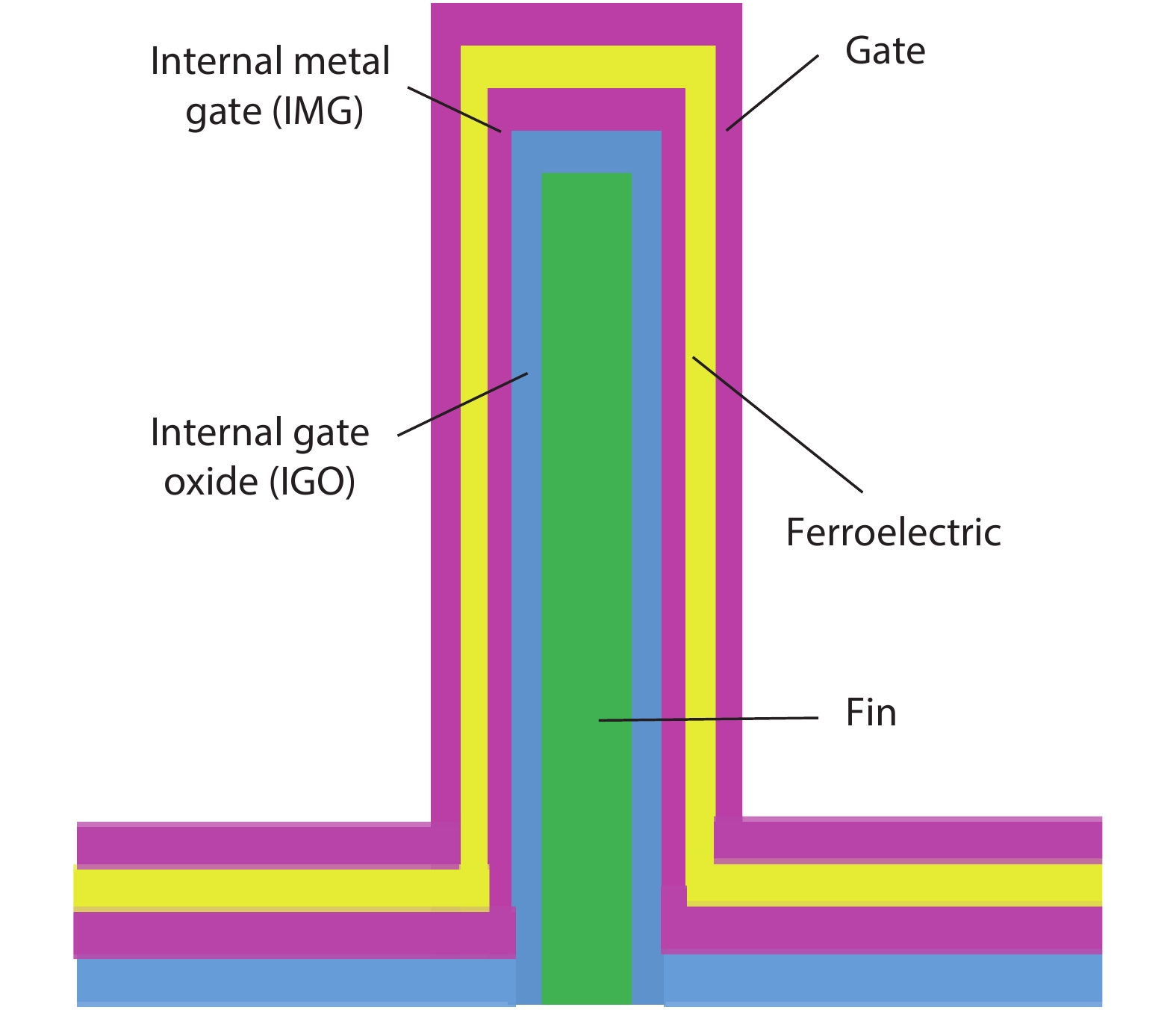
Processing math: 100%
J. Semicond. > 2020, Volume 41 > Issue 6 > 062403

ARTICLES

Variation tolerance for high-speed negative capacitance FinFET SRAM bit cell

Yaqian Qian1, , Shushan Qiao1, 2, and Rongqiang Yang1

+ Author Affiliations

 Corresponding author: Yaqian Qian and Rongqiang Yang authors are with the Department of Electronic and Communication Engineering, University of Chinese Academy of Science, Beijing, China (e-mail: qianyaqian17@mails.ucas.ac.cn); Shushan Qiao author is with the Institute of Micro-electronics of the Chinese Academy of Sciences (IMECAS), Beijing, China (e-mail: Qiaoshushan@ime.ac.cn)

DOI: 10.1088/1674-4926/41/6/062403

PDF

Turn off MathJax

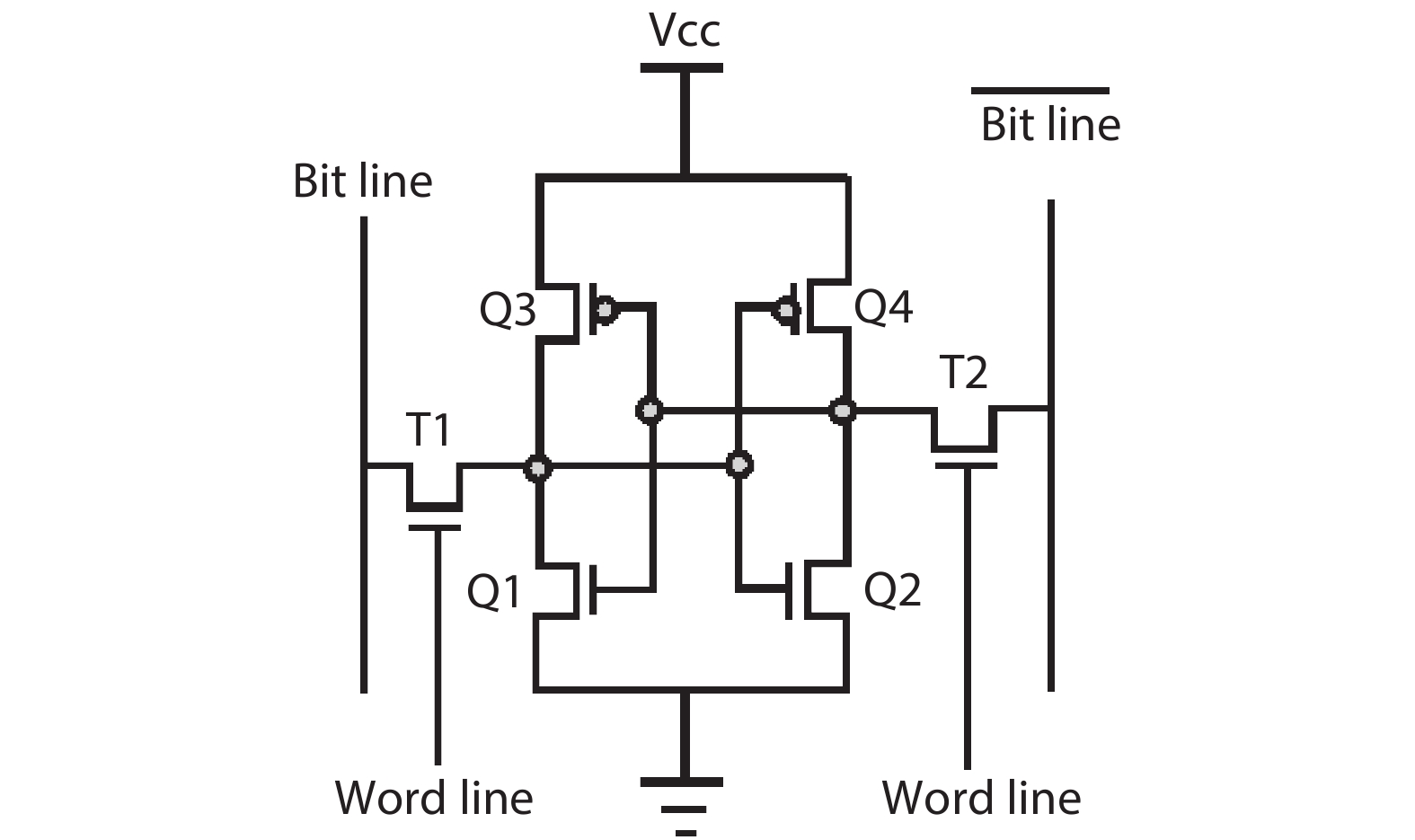
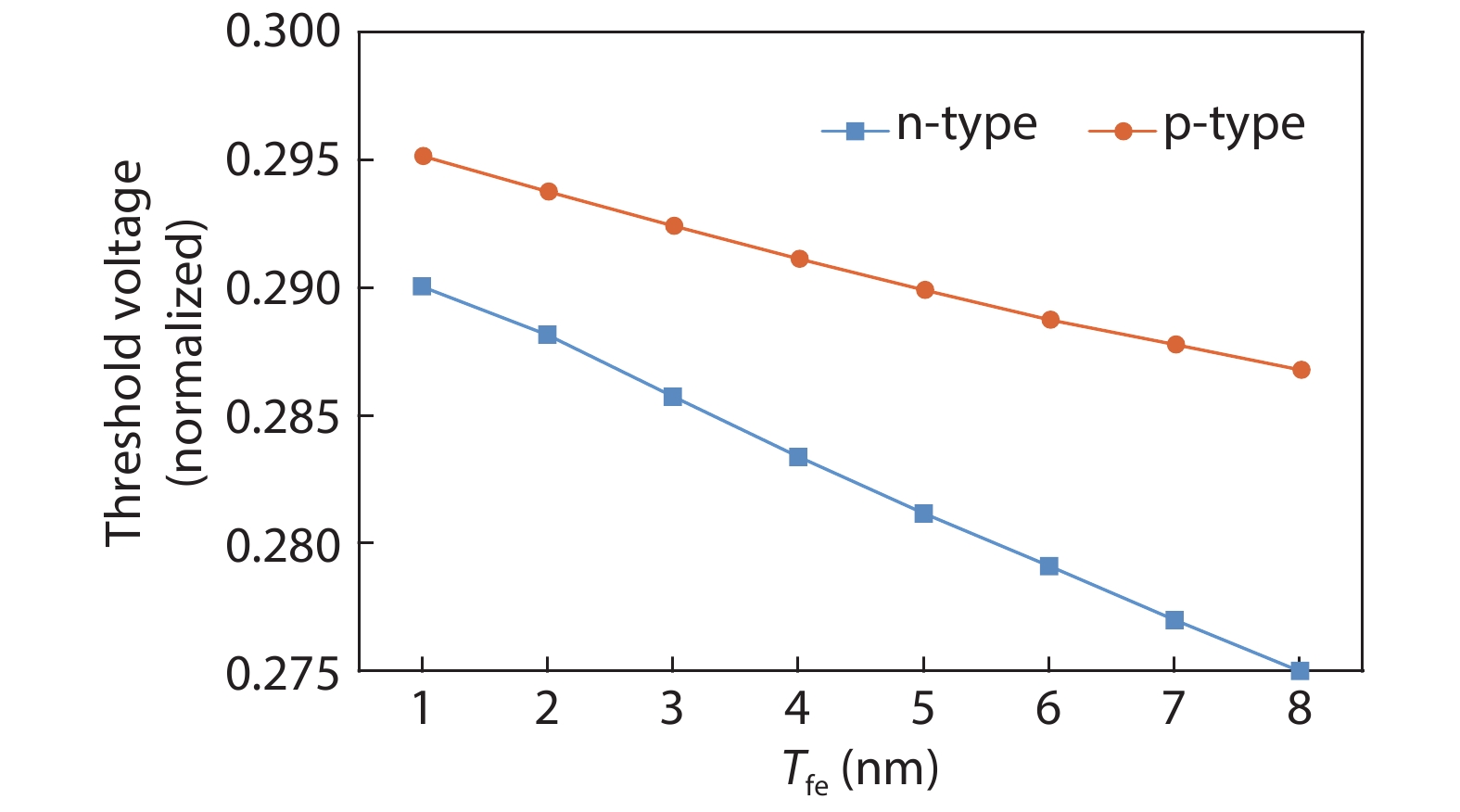
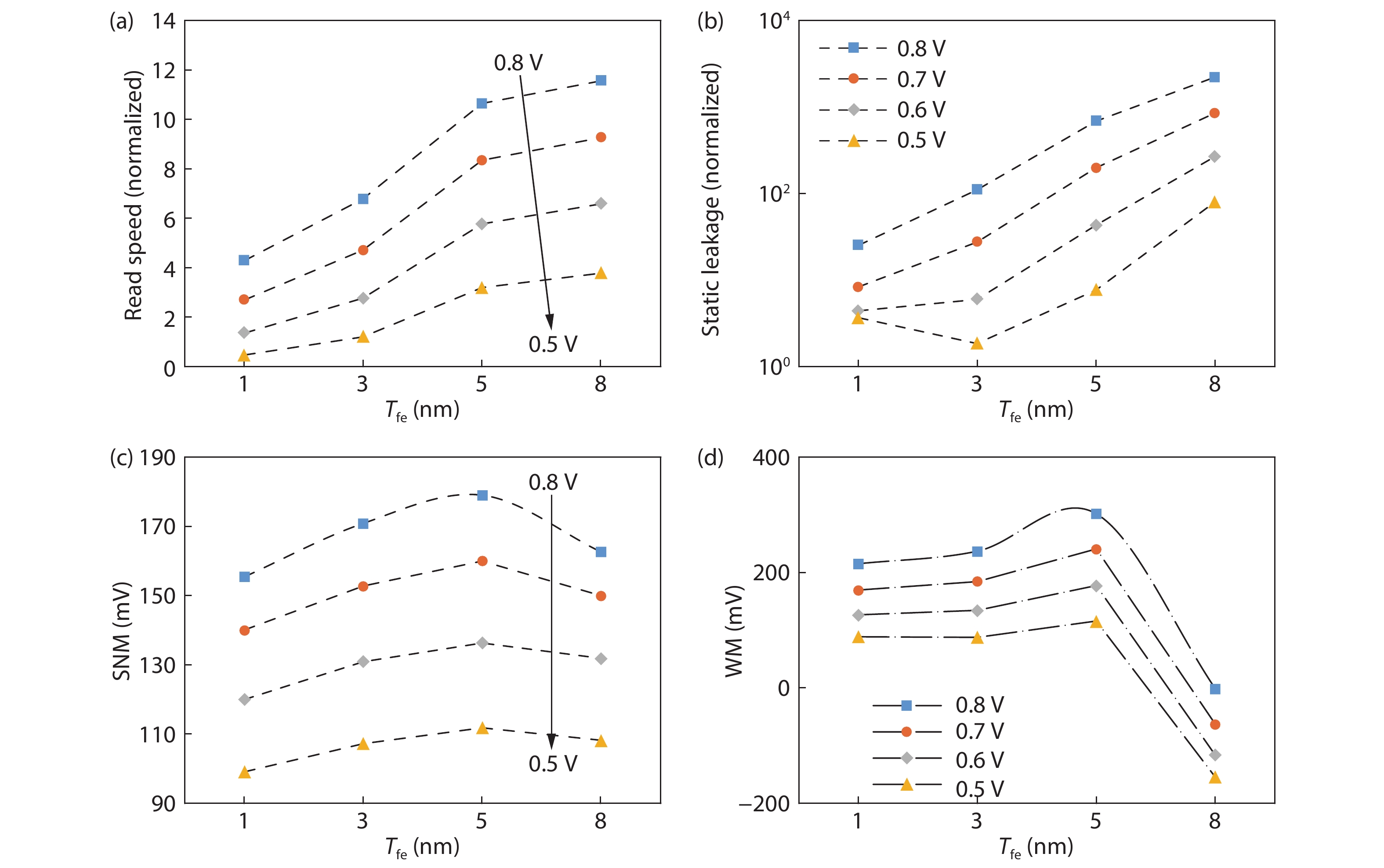
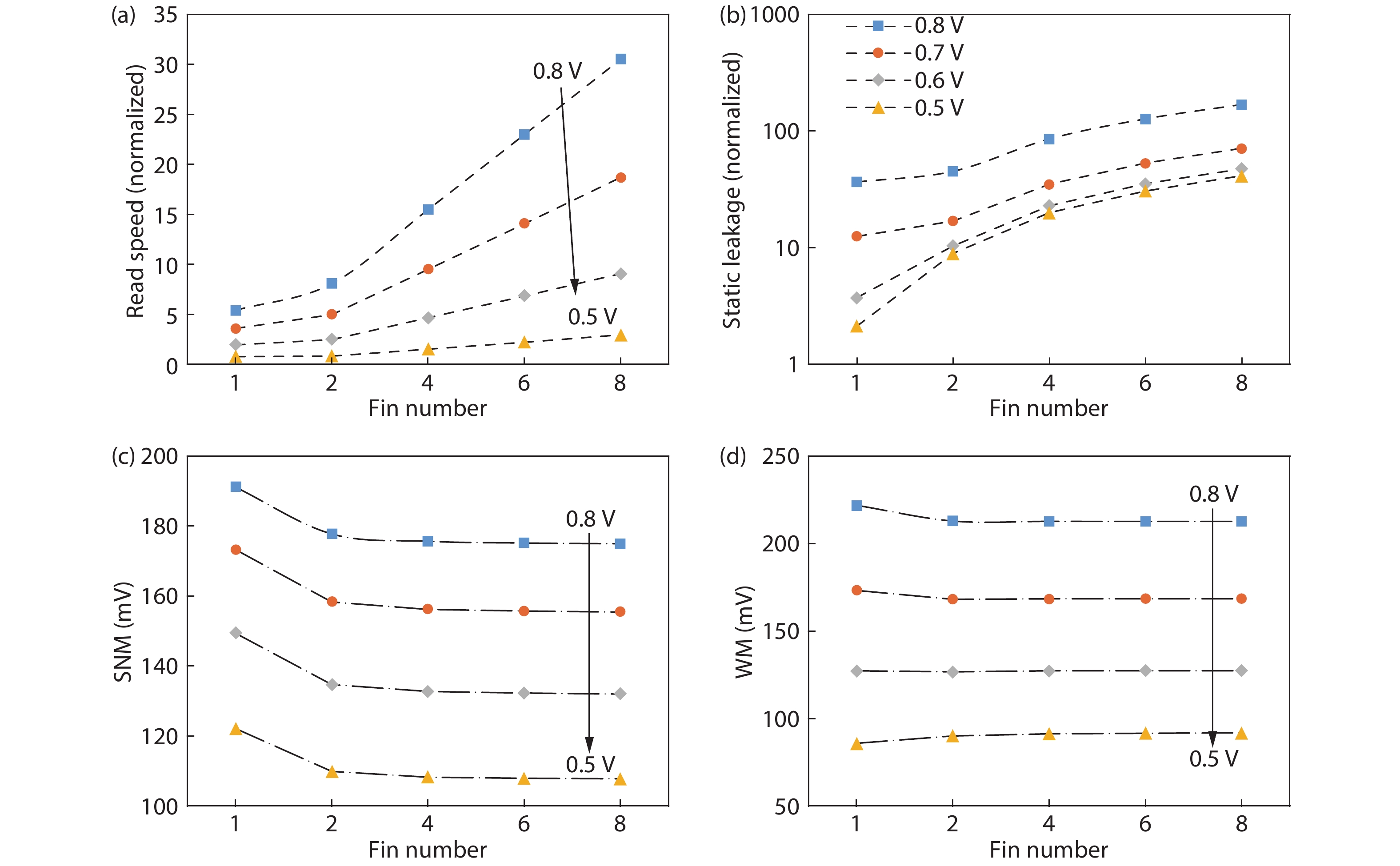
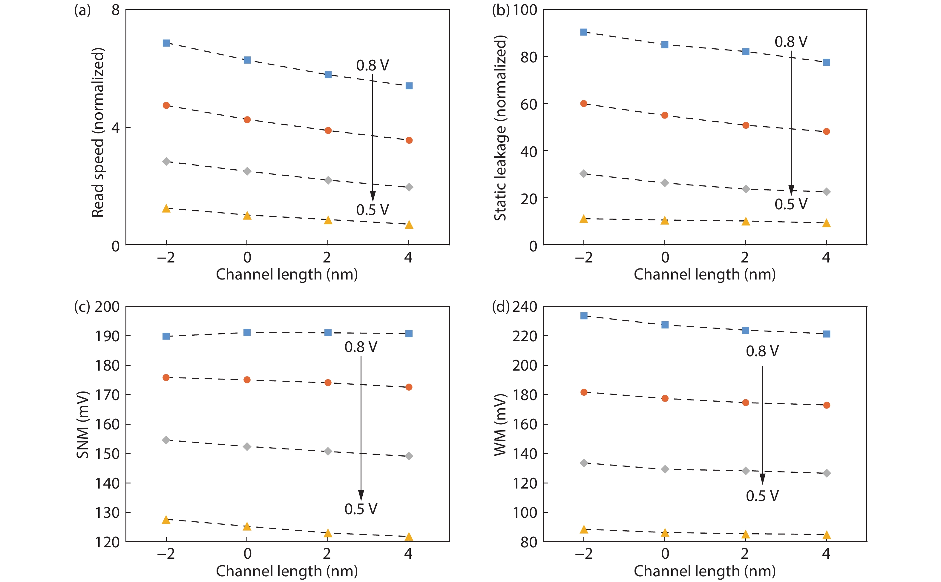
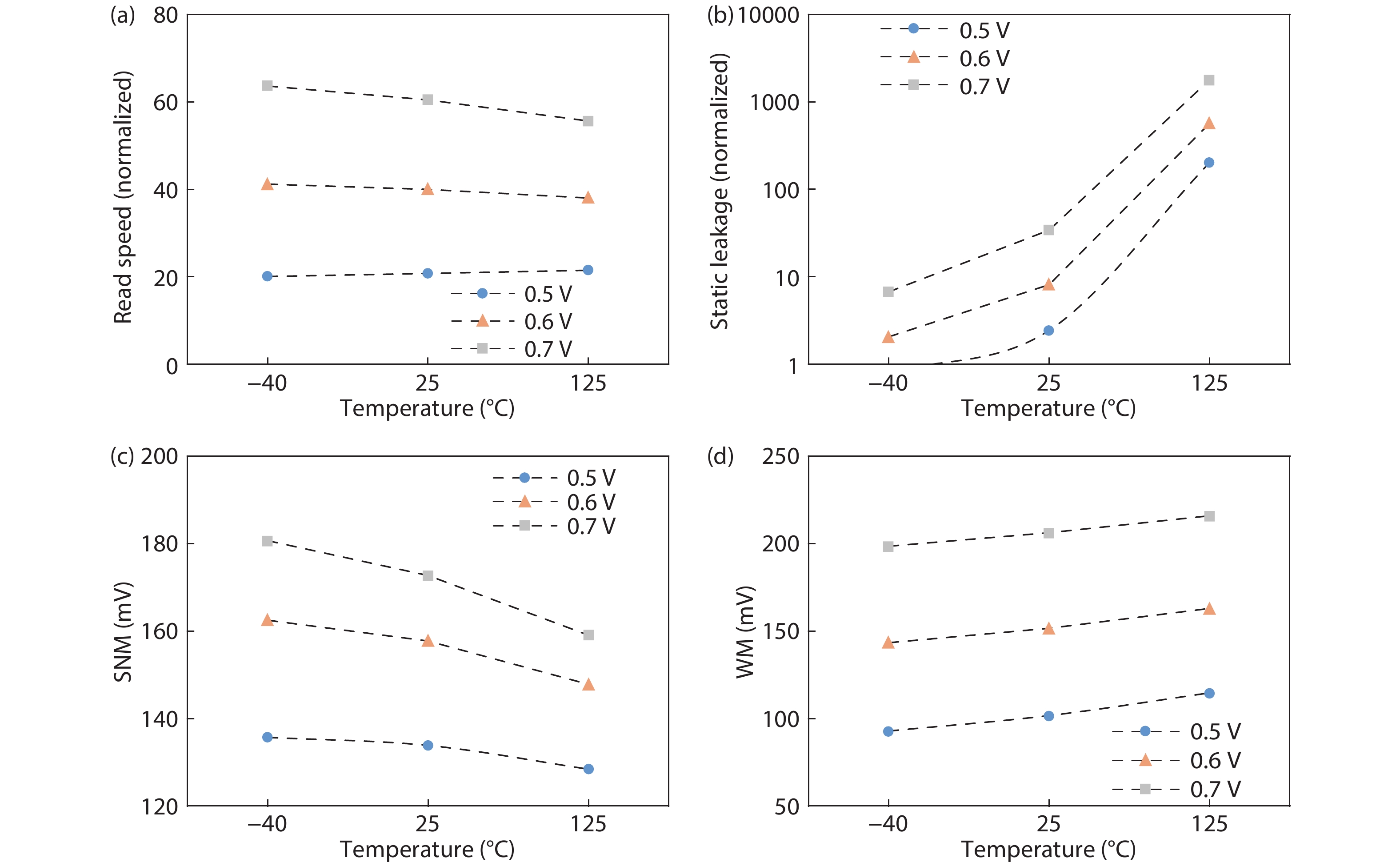
Abstract: Negative capacitance FinFET (NC-FinFET) has a promising developmental prospect due to its superior performance in SS < 60 mV/dec (subthreshold swing), especially in SRAM. Noise margin is an important metric to evaluate the performance for SRAM, together with static leakage, read speed, etc. In this paper, we study the effects of the variation of ferroelectric material (thickness, polarization), FinFET critical physical parameters (fin number, channel length) and some ambient factors (working temperature, supply voltage) on the performance of NC-FinFET SRAM within the reasonable fluctuation tolerance range. The SRAM bit cell is analyzed with a basic 6T structure. The impact of fin number and channel length for NC-FinFET SRAM is different from that of conventional FinFETs. Additionally, the ferroelectric material and some other factors are assessed in detail.

Key words: negative-capacitance FinFET (NC-FinFET) SRAMvariationnoise marginspeed

The structure of NC-FinFETs is almost the same as FinFETs, but the NC layer is positioned between the gate and internal gate, whose structure is MFMIS (metal–ferroelectric–metal–insulator–semiconductor) as shown in Fig. 1[1]. Compared to another structure — MFIS (metal–ferroelectric–insulator–semiconductor), it can effectively avoid hysteresis under most cases. Negative capacitance FinFETs (NC-FinFETs) could operate at a sub-60-mv/dec subthreshold swing, as shown in Fig. 2, and a high on-current[2]. Articles[35] have introduced the compact model consisting of BSIM-CMG and Landau-Khalatnikov (L-K) equations, simulation flows, and characteristics of NC-FinFET, especially in Ref. [6], for a single transistor. The variation of ferroelectric material and some parasitic factors have been deeply analyzed, but the variation tolerance for cell level has not been estimated. As SRAMs occupy a major portion of chip area, a new study to replace FinFETs with NC-FinFETs is meaningful. Two factors: static noise margin (SNM) and write margin (WM) are the main metrics to evaluate the performance of SRAM, and the trade-off between them has always existed. Besides, to estimate the standby state, leakage measurement is essential.

Figure  1.  (Color online) the structure of NC-FinFET.
Figure  2.  (Color online) The subthreshold swing improved by NC compared to the baseline.

In this paper, we study the effects of the variation of ferroelectric material (thickness, polarization), FinFET critical physical parameters (fin number, channel length) and some ambient factors (working temperature, supply voltage) on the performance of NC-FinFET SRAM with high read speed.

Fig. 3 is a schematic of a traditional 6T bit-cell consisting of NC-FinFETs. This paper will study the performance of SRAM based on the above structure, how to analyze the internal factors and find a better balance will be carried out through the simulation process of Fig. 4. Firstly, the ferroelectric materials commonly used in NCFETs are perovskite ferroelectrics. These materials have good stability. The local temperature is about 500 °C. Therefore, even at high temperatures of 125 °C, The negative capacitance characteristics remain the same, and the performance will not abruptly change due to this temperature. Static noise margin (SNM) is the term used to determine the stability of the SRAM cells. The SNM is the tolerance of the maximum noise voltage for the cross inverters output nodes and the minimum amount of noise to ensure the state is maintained[7]. For the simulation graphic, SNM is defined as the side of the smaller square that can be fitted inside the "eye" of the butterfly stability. Large SNM means the cell will not be disturbed easily during the read operation. The write margin (WM) is the maximum bit-line voltage to flip the node from 1 to 0[8]. The larger the WM is, the faster the write speed will be. SNM and WM are separately associated with the ratios of pass gate transistor (PG), pass down transistor (PD) and pull up transistor (PU) on-currents, the former can be presented as Ion_PGIon_PD, and the latter as Ion_PDIon_PU. The drive voltage and current are difficult to control because of the variation of a single device, so by modifying the negative capacitance material, the basic features of the FinFET or the other conditions, the performance of SRAM will be quite distinguishable.

Figure  3.  The schematic of traditional 6T SRAM-cell.
Figure  4.  The simulation flow chart for analysis the performance variation for the 6T SRAM, and the compact model is the BSIM-CMG cooperating L-K equations.

Even under the same process, n-type and p-type transistors present different performances, especially the threshold voltage (VT). Fig. 5 confirms the above conclusions. It can be seen that as the thickness of the ferroelectric increases, the VT mismatch between the two transistors becomes more serious. The threshold voltage of the ferroelectric material is negative, so the VT of a NC-FinFET will be lower compared to the baseline FinFET. The threshold voltage of the device is the minimum voltage required to turn on the transistor, which is closely related to the gate control capability of the device itself. The study of this work is based on the actual taped-out FinFET data, the mismatch between n-type and p-type transistors is small, but as Tfe increases, the VT variation degree of the two is not consistent due to the difference of the carrier transport mechanism between them. The grid-control capability of n-type NC-FinFETs will become weaker with the increase of ferroelectric thickness, while the p-type will be relatively slow. So, as the Tfe increases, the VT mismatch will increase. In order to observe the tolerance variation on cell level, the same change will be applied for the whole SRAM cell. To evaluate the stability of NC-FinFET SRAM cells, first of all, under a fixed FinFET baseline and working environment, by changing the ferroelectric material the single transistor showed that as the thickness of the ferroelectric decreased, the negative DIBL phenomenon will be more apparent. A suitable choice of polarization is difficult to a certain extent, so in this work we refer to the parameters in paper[9]. Having found appropriate NC parameters, the modification for the baseline FinFET is carried on to determine whether or not the changing trend of NC-FinFET SRAM is similar to the baseline FinFET SRAM. Increasing fin number to boost the drive current of SRAM is the industry technique, so changing the fin number in cooperation with baseline SRAM will be verified. Furthermore, a perfect channel length could be optimized in a different technology generation, and this factor will also be analyzed. Finally, we will discuss some other impact after discovering the best parameters for NC-FinFET SRAM. In Ref. [10], conclusions can be drawn that the SNM of SRAM tends to decrease with the increasing temperature, and the WM shows the opposite tendency. Besides, the supply voltage is limited. Although a large drive voltage is beneficial to speed, it will lead to the power consumption of the SRAM cell increasing exponentially. Therefore we will find out the smallest supply voltage for NC-FinFET SRAM to work normally.

Figure  5.  (Color online) The VT mismatch between n-type and p-type NC-FinFET under the same process: when the thickness of ferroelectric material increases, the mismatch gets worse.

Followed by all the above simulation flows, some phenomena can be observed from the graphs. Firstly, we will study the integration of ferroelectric material and basic FinFET even though the polarization is difficult to extract from the figure, while the recently proposed SPICE model of ferroelectric material in Ref. [11] utilizes a very complex circuit to express the nonlinear dependence of VFE upon polarization (P). P is self-consistently equal to gate charge (Qg) of the FinFET. Hence, the model is independent of FinFET parameters[12]. We choose the appropriate parameters to make sure the ferroelectric works well. Considering the industry process, unitive (uniform) change will be implemented in the whole SRAM cell consisting of different transistors. Secondly, the larger thickness of the ferroelectric material (Tfe) improves the read speed distinctly as has been shown in Fig. 6(a). An explanation for this phenomenon is that the ferroelectric works perfectly with the baseline in a reasonable range and the conclusions related with Tfe in Ref. [13] are almost the same. The influences on other performances—static leakage, SNM and WM—is shown in Figs. 6(b)6(d). The changing tendency between static leakage and Tfe is same, so a small thickness is needed for ultra-low power SRAM. Differing from the single change trend, the SNM and WM is fluctuant with increasing Tfe. When the thickness of the ferroelectric is 5 nm, SNM reaches its maximum value. As the thickness of the ferroelectrics continues to increase, SNM decreases; the main cause of this phenomenon is the large VT mismatch in SRAM. Consistent with the trend of SNM, WM shows a declining trend when Tfe equals 5 nm. In order to avoid an unstable state, 1 to 3 nm is the best choice. In this range, the SNM and WM is relatively balanced without a large trade-off between them. The formula is listed to further investigate the influence of Tfe to the cell:

Figure  6.  (Color online) (a) Read speed, (b) leakage, (c) SNM, and (d) WM of NC-FinFET SRAM influenced by the thickness of ferroelectric material.
Vfe=2αfetfeQfe+4βfetfeQ3fe+6γfetfeQ5fe+ρfetfedQgdt,
(1)
Cfe=12αfetfe+12βfetfeQ2fe+30γfetfeQ4fe.
(2)

Refs. [14, 15] explain that the CFE should be a little larger than Cbaseline, and the large discrepancy will lead to a mismatch between negative capacitance and FinFET capacitance, while the coefficient is fixed, so the thicker the ferroelectric material becomes, more serious the mismatch problem will be. The work function is associated with the gate structure, so the relationship between ferroelectric and baseline needs further research. Furthermore, the reliability is still unclear.

Secondly, having fixed the parameters of ferroelectric material, in this part, we have analyzed the critical metrics of the baseline. As with the above operation, all the changes are the same for the whole SRAM cell. Increasing the fin number (Nfin) of the NC-SRAM cell, the influences basically conforms to the baseline. In detail, read speed is remarkably improved since the increase of Nfin contributes to the current, as shown in Fig. 7(a). Meanwhile, in Fig. 7(b), the leakage problem gets worse because increasing the fin number is equivalent to making the width longer, resulting in the leakage path being broadened. Some other metrics are shown in Figs. 7(c) and 7(d), the change of SNM and WM is not evident, but we can still see that when the fin number is only 1, both of them are better. The tendency is not parallel to the baseline, so the fin number of NC-FinFET should harmonize with the baseline SRAM cell. Another parameter: channel length (Lg) is also vital to the NC-FinFET SRAM cell. In principle, the read speed will slow down while the Lg increases for the reason that the voltage and current controlled by gate is enhanced in a short-channel device. The NC-SRAM cell optimizes the read speed well obeying the above rules. In the cell level, the leakage problem is presented in Fig. 8(b), the leakage problem is gradually improved because the short channel will lead to larger junction leakage. The more detail causes can be deduced from the formula[16]:

Figure  7.  (Color online) (a) Read speed, (b) leakage, (c) SNM, and (d) WM of NC-FinFET SRAM influenced by the fin number of baseline with fixed FE thickness 3 nm.
Figure  8.  (Color online) (a) Read speed, (b) leakage, (c) SNM, and (d) WM of NC-FinFET SRAM influenced by the channel length of baseline with one fin.
Istandby=Isub(PU)+Isub(PD)+Isub(PG)+Igate(PU)+Igate(PD)+Igate(PG)+Ijunc(PU)+Ijunc(PD) +3Ijunc(PG).
(3)

In the formula, the factor most severely influenced by length is Ijunction. So, to some extent, the correspondence between the ferroelectric material and baseline mainly account for the leakage, which means the channel length determines the static power of the cell. From Fig. 8(c), the SNM is almost maintained under the same voltage, but a little abnormal phenomenon occurs when the supply voltage is 0.8 V. To account for this, the SNM can be expressed[17]:

SNM6T=VT1K+1×[VDD2r+1r+1VT1+rK(r+1)VDD2VT1+Krq+rq(1+2k+rqk2)],
(4)
r=ratio=βdβa,
(5)
q=βpβa,
(6)
k=rr+1(r+1r+1v2svr21),
(7)
vs=VDDVT,
(8)
Vr=vsrVTr+1.
(9)

In this paper, the size of the PD, PU and PG are all the same, so r and q are equal to 1. To analyze the influence of the channel length for SNM, the VDD will be fixed to 0.8 V, then we get following formula:

SNM6T=VT0.8(3k+2)2VT(2k+1)4(k+1)(2+k),
(10)
k=1222(0.8VT0.832VT)21.
(11)

The conclusion can be drawn that in this case, SNM has the same change tendency with the VT, while VT is almost determined by channel length. So the VT reflects the SNM. Conversely, the WM drops mildly. From all of above, the channel length is not only important to the baseline SRAM but also sensitive to the NC-FinFET SRAM. An appropriate channel length maybe the key factor for the whole NC-FinFET SRAM. Apart from that, in all figures the supply voltage also affects the performance. Most of the metrics conform to normal rules except SNM and WM under special cases. The range of supply voltages ensuring the NC-FinFET SRAM works correctly will be discussed after fixing all the above parameters with best choice. From all the graphics, the best voltage for the cell can be chosen between 0.5 to 0.7 V, making low power significant. Fig. 9 presents the temperature infection. It has been mentioned the structure chosen in this article is MFMIS. The interconnection between the metallic and ferroelectric layers is based on the principle of self-continuity of charge, because the ferroelectric layer and the metal layer share only charge, but the material itself is not compatible. When the temperature is 125 °C, the ferroelectric remains stable and the metal layer will not migrate. Therefore, under reasonably high temperature, the device itself is in a stable state. Read speed is almost flat while static leakage abruptly rises under higher temperature. The SNM declines slightly while WM increases gently.

Figure  9.  (Color online) (a) Read speed, (b) leakage, (c) SNM, and (d) WM of NC-FinFET SRAM influenced by temperature with one fin and supply voltage ranges from 0.5 to 0.7 V.

Based on an ordinary and reasonably proper SPICE model of ferroelectrics, the performance of a NC-FinFET SRAM cell is presented. We discussed the variation tolerance for the NC-FinFET SRAM cell. A small Tfe ranging from 1 to 3 nm exhibits a better performance while sacrificing little speed. Small Nfin is the better choice in this paper due to the fact that SNM and WM barely change when the fin number increases but the leakage problem becomes serious. Channel length is limited to within 6 nm, due to the fact that trade-off among leakage, SNM and WM cannot be eliminated, except under small channel length, and the read speed and WM is perfect while the leakage problem can be cleaned up by making NC-FinFET SRAM work under a low supply voltage. Therefore, a reasonable supply voltage range is 0.5 to 0.7 V. This work utilizes its low power advantage meanwhile ensuring performance. Considering the application in industry, both low and high temperatures can be tolerated, ranging from –40 to 125 °C which is the detection range commonly used in process.

This work was supported in part by the University of Chinese Academy of Science and SMIC


[1]
Li K, Chen P, Lai T, et al. Sub-60mV-swing negative-capacitance FinFET without hysteresis. IEEE International Electron Devices Meeting (IEDM), 2015, 22
[2]
Lin C, Khan A I, Salahuddin S, et al. Effects of the variation of ferroelectric properties on negative capacitance FET characteristics. IEEE Trans Electron Devices, 2016, 63(5), 21972199 doi: 10.1109/TED.2016.2514783
[3]
Khandelwal S, Khan A I, Duarte J P, et al. Circuit performance analysis of negative capacitance FinFETs. IEEE Symposium on VLSI Technology, 2016, 1
[4]
Ko E, Lee H, Goh Y, et al. Sub-60-mV/decade negative capacitance FinFET with sub-10-nm hafnium-based ferroelectric capacitor. IEEE J Electron Devices Soc, 2017, 5(5), 306309 doi: 10.1109/JEDS.2017.2731401
[5]
Ota H, Fukuda K, Ikegami T, et al. Perspective of negative capacitance FinFETs investigated by transient TCAD simulation. IEEE International Electron Devices Meeting (IEDM), 2017, 15
[6]
Khandelwal S, Duarte J P, Khan A I, et al. Impact of parasitic capacitance and ferroelectric parameters on negative capacitance FinFET characteristics. IEEE Electron Device Lett, 2017, 38(1), 142144 doi: 10.1109/LED.2016.2628349
[7]
Banga H, Agarwal D. Single bit-line 10T SRAM cell for low power and high SNM. International Conference on Recent Innovations in Signal processing and Embedded Systems (RISE), 2017, 433
[8]
Zhang G, Li Y, Yu S F. Techniques to improve read noise margin and write margin for bit-cell of 14 nm FINFET node. China Semiconductor Technology International Conference, 2015, 1
[9]
Chen K T, Gu S S, Lee M H. Ferroelectric HfZrO xFETs on SOI substrate with reverse-DIBL (drain-induced barrier lowering) and NDR (negative differential resistance). IEEE J Electron Devices Soc, 2018, 6, 900904 doi: 10.1109/JEDS.2018.2863283
[10]
Aziz A, Ghos S, Datta S, et al. Physics-based circuit compatible SPICE model for ferroelectric transistors. IEEE Electron Device Lett, 2016, 37(6), 805808 doi: 10.1109/LED.2016.2558149
[11]
Kumar V, Shrivatava R K, Padaliya M M. A temperature compensated read assist for low Vmin and high performance high density 6T SRAM in FinFET technology. 2018 31st International Conference on VLSI Design and 2018 17th International Conference on Embedded Systems (VLSID), 2018, 447
[12]
Li Y, Yao K, Samudra G S. Delay and power evaluation of negative capacitance ferroelectric MOSFET based on SPICE model. IEEE Trans Electron Devices, 2017, 64(5), 24032408 doi: 10.1109/TED.2017.2674020
[13]
Dutta T, Pahwa G, Trivedi A R, et al. performance evaluation of 7-nm node negative capacitance FinFET-based SRAM. IEEE Electron Device Lett, 2017, 38(8), 1161 doi: 10.1109/LED.2017.2712365
[14]
Pahwa G, Dutta T, Agarwal A, et al. Analysis and compact modeling of negative capacitance transistor with high on-current and negative output differential resistance —Part I: model description. IEEE Trans Electron Devices, 2016, 63(12), 4981 doi: 10.1109/TED.2016.2614432
[15]
Pahwa G, Dutta T, Agarwal A, et al. Analysis and compact modeling of negative capacitance transistor with high on-current and negative output differential resistance—Part II: model validation. IEEE Trans Electron Devices, 2016, 63(12), 4986 doi: 10.1109/ted.2016.2614436
[16]
Dong Q, Ma Y N, Chen H, et al. A novel method for accurate measurement and decoupling of SRAM standby leakage. IEEE 11th International Conference on Solid-State and Integrated Circuit Technology, 2012, 1
[17]
Prasad G, Kusuma R. Statistical (M-C) and static noise margin analysis of the SRAM cells. Students Conference on Engineering and Systems (SCES), 2013, 1
Fig. 1.  (Color online) the structure of NC-FinFET.

Fig. 2.  (Color online) The subthreshold swing improved by NC compared to the baseline.

Fig. 3.  The schematic of traditional 6T SRAM-cell.

Fig. 4.  The simulation flow chart for analysis the performance variation for the 6T SRAM, and the compact model is the BSIM-CMG cooperating L-K equations.

Fig. 5.  (Color online) The VT mismatch between n-type and p-type NC-FinFET under the same process: when the thickness of ferroelectric material increases, the mismatch gets worse.

Fig. 6.  (Color online) (a) Read speed, (b) leakage, (c) SNM, and (d) WM of NC-FinFET SRAM influenced by the thickness of ferroelectric material.

Fig. 7.  (Color online) (a) Read speed, (b) leakage, (c) SNM, and (d) WM of NC-FinFET SRAM influenced by the fin number of baseline with fixed FE thickness 3 nm.

Fig. 8.  (Color online) (a) Read speed, (b) leakage, (c) SNM, and (d) WM of NC-FinFET SRAM influenced by the channel length of baseline with one fin.

Fig. 9.  (Color online) (a) Read speed, (b) leakage, (c) SNM, and (d) WM of NC-FinFET SRAM influenced by temperature with one fin and supply voltage ranges from 0.5 to 0.7 V.

[1]
Li K, Chen P, Lai T, et al. Sub-60mV-swing negative-capacitance FinFET without hysteresis. IEEE International Electron Devices Meeting (IEDM), 2015, 22
[2]
Lin C, Khan A I, Salahuddin S, et al. Effects of the variation of ferroelectric properties on negative capacitance FET characteristics. IEEE Trans Electron Devices, 2016, 63(5), 21972199 doi: 10.1109/TED.2016.2514783
[3]
Khandelwal S, Khan A I, Duarte J P, et al. Circuit performance analysis of negative capacitance FinFETs. IEEE Symposium on VLSI Technology, 2016, 1
[4]
Ko E, Lee H, Goh Y, et al. Sub-60-mV/decade negative capacitance FinFET with sub-10-nm hafnium-based ferroelectric capacitor. IEEE J Electron Devices Soc, 2017, 5(5), 306309 doi: 10.1109/JEDS.2017.2731401
[5]
Ota H, Fukuda K, Ikegami T, et al. Perspective of negative capacitance FinFETs investigated by transient TCAD simulation. IEEE International Electron Devices Meeting (IEDM), 2017, 15
[6]
Khandelwal S, Duarte J P, Khan A I, et al. Impact of parasitic capacitance and ferroelectric parameters on negative capacitance FinFET characteristics. IEEE Electron Device Lett, 2017, 38(1), 142144 doi: 10.1109/LED.2016.2628349
[7]
Banga H, Agarwal D. Single bit-line 10T SRAM cell for low power and high SNM. International Conference on Recent Innovations in Signal processing and Embedded Systems (RISE), 2017, 433
[8]
Zhang G, Li Y, Yu S F. Techniques to improve read noise margin and write margin for bit-cell of 14 nm FINFET node. China Semiconductor Technology International Conference, 2015, 1
[9]
Chen K T, Gu S S, Lee M H. Ferroelectric HfZrO xFETs on SOI substrate with reverse-DIBL (drain-induced barrier lowering) and NDR (negative differential resistance). IEEE J Electron Devices Soc, 2018, 6, 900904 doi: 10.1109/JEDS.2018.2863283
[10]
Aziz A, Ghos S, Datta S, et al. Physics-based circuit compatible SPICE model for ferroelectric transistors. IEEE Electron Device Lett, 2016, 37(6), 805808 doi: 10.1109/LED.2016.2558149
[11]
Kumar V, Shrivatava R K, Padaliya M M. A temperature compensated read assist for low Vmin and high performance high density 6T SRAM in FinFET technology. 2018 31st International Conference on VLSI Design and 2018 17th International Conference on Embedded Systems (VLSID), 2018, 447
[12]
Li Y, Yao K, Samudra G S. Delay and power evaluation of negative capacitance ferroelectric MOSFET based on SPICE model. IEEE Trans Electron Devices, 2017, 64(5), 24032408 doi: 10.1109/TED.2017.2674020
[13]
Dutta T, Pahwa G, Trivedi A R, et al. performance evaluation of 7-nm node negative capacitance FinFET-based SRAM. IEEE Electron Device Lett, 2017, 38(8), 1161 doi: 10.1109/LED.2017.2712365
[14]
Pahwa G, Dutta T, Agarwal A, et al. Analysis and compact modeling of negative capacitance transistor with high on-current and negative output differential resistance —Part I: model description. IEEE Trans Electron Devices, 2016, 63(12), 4981 doi: 10.1109/TED.2016.2614432
[15]
Pahwa G, Dutta T, Agarwal A, et al. Analysis and compact modeling of negative capacitance transistor with high on-current and negative output differential resistance—Part II: model validation. IEEE Trans Electron Devices, 2016, 63(12), 4986 doi: 10.1109/ted.2016.2614436
[16]
Dong Q, Ma Y N, Chen H, et al. A novel method for accurate measurement and decoupling of SRAM standby leakage. IEEE 11th International Conference on Solid-State and Integrated Circuit Technology, 2012, 1
[17]
Prasad G, Kusuma R. Statistical (M-C) and static noise margin analysis of the SRAM cells. Students Conference on Engineering and Systems (SCES), 2013, 1
1

Analytical model for the effects of the variation of ferrolectric material parameters on the minimum subthreshold swing in negative capacitance capacitor

Raheela Rasool, Najeeb-ud-Din, G. M. Rather

Journal of Semiconductors, 2019, 40(12): 122401. doi: 10.1088/1674-4926/40/12/122401

2

Study of the effect of switching speed of the a-SiC/c-Si (p)-based, thyristor-like, ultra-high-speed switches, using two-dimensional simulation techniques

Evangelos I. Dimitriadis, Nikolaos Georgoulas

Journal of Semiconductors, 2017, 38(5): 054001. doi: 10.1088/1674-4926/38/5/054001

3

Substrate temperature effect on the photophysical and microstructural properties of fluorine-doped tin oxide nanoparticles

Ibiyemi Abideen, Yusuf Gbadebo, Faremi Abass

Journal of Semiconductors, 2017, 38(7): 072001. doi: 10.1088/1674-4926/38/7/072001

4

Impact of underlap spacer region variation on electrostatic and analog performance of symmetrical high-k SOI FinFET at 20 nm channel length

Neeraj Jain, Balwinder Raj

Journal of Semiconductors, 2017, 38(12): 122002. doi: 10.1088/1674-4926/38/12/122002

5

Large signal and noise properties of heterojunction AlxGa1-xAs/GaAs DDRIMPATTs

Suranjana Banerjee, Monojit Mitra

Journal of Semiconductors, 2016, 37(6): 064002. doi: 10.1088/1674-4926/37/6/064002

6

The impact of process variations on input impedance and mitigation using a circuit technique in FinFET-based LNA

D. Suresh, K. K. Nagarajan, R. Srinivasan

Journal of Semiconductors, 2015, 36(4): 045002. doi: 10.1088/1674-4926/36/4/045002

7

Line-edge roughness induced single event transient variation in SOI FinFETs

Weikang Wu, Xia An, Xiaobo Jiang, Yehua Chen, Jingjing Liu, et al.

Journal of Semiconductors, 2015, 36(11): 114001. doi: 10.1088/1674-4926/36/11/114001

8

A novel DTSCR with a variation lateral base doping structure to improve turn-on speed for ESD protection

Jizhi Liu, Zhiwei Liu, Ze Jia, Juin. J Liou

Journal of Semiconductors, 2014, 35(6): 064010. doi: 10.1088/1674-4926/35/6/064010

9

Parameters influencing the optical properties of SnS thin films

Priyal Jain, P. Arun

Journal of Semiconductors, 2013, 34(9): 093004. doi: 10.1088/1674-4926/34/9/093004

10

Flicker and thermal noise in an n-channel underlap DG FinFET in a weak inversion region

Sudhansu Kumar Pati, Hemant Pardeshi, Godwin Raj, N Mohankumar, Chandan Kumar Sarkar, et al.

Journal of Semiconductors, 2013, 34(2): 024002. doi: 10.1088/1674-4926/34/2/024002

11

A process/temperature variation tolerant RSSI

Lei Qianqian, Lin Min, Shi Yin

Journal of Semiconductors, 2012, 33(12): 125010. doi: 10.1088/1674-4926/33/12/125010

12

MOS Capacitance-Voltage Characteristics II. Sensitivity of Electronic Trapping at Dopant Impurity from Parameter Variations

Jie Binbin, Sah Chihtang

Journal of Semiconductors, 2011, 32(12): 121001. doi: 10.1088/1674-4926/32/12/121001

13

Design of high speed LVDS transceiver ICs

Xu Jian, Wang Zhigong, Niu Xiaokang

Journal of Semiconductors, 2010, 31(7): 075014. doi: 10.1088/1674-4926/31/7/075014

14

An asymmetrical sensing scheme for 1T1C FRAM to increase the sense margin

Jia Ze, Zou Zhongren, Ren Tianling, Chen Hongyi

Journal of Semiconductors, 2010, 31(11): 115001. doi: 10.1088/1674-4926/31/11/115001

15

A 2.4 GHz high-linearity low-phase-noise CMOS LC-VCO based on capacitance compensation

Li Zhenrong, Zhuang Yiqi, Li Bing, Jin Gang, Jin Zhao, et al.

Journal of Semiconductors, 2010, 31(7): 075005. doi: 10.1088/1674-4926/31/7/075005

16

Temperature coefficients of grain boundary resistance variations in a ZnO/p-Si heterojunction

Liu Bingce, Liu Cihui, Xu Jun, Yi Bo

Journal of Semiconductors, 2010, 31(12): 122001. doi: 10.1088/1674-4926/31/12/122001

17

A cross-coupled-structure-based temperature sensor with reduced process variation sensitivity

Tie Meng, Cheng Xu

Journal of Semiconductors, 2009, 30(4): 045002. doi: 10.1088/1674-4926/30/4/045002

18

A fast-settling frequency-presetting PLL frequency synthesizer with process variation compensation and spur reduction

Yan Xiaozhou, Kuang Xiaofei, Wu Nanjian

Journal of Semiconductors, 2009, 30(4): 045007. doi: 10.1088/1674-4926/30/4/045007

19

High-Speed,Robust CMOS Dynamic Circuit Design

Lai Lianzhang, Tang Tingao, Lin Yinyin

Chinese Journal of Semiconductors , 2006, 27(6): 1006-1011.

20

3-D Simulation of FINFET

LIU En-feng, LIU Xiao-yan, HAN Ru-qi

Chinese Journal of Semiconductors , 2002, 23(9): 909-913.

  • Search

    Advanced Search >>

    GET CITATION

    Yaqian Qian, Shushan Qiao, Rongqiang Yang. Variation tolerance for high-speed negative capacitance FinFET SRAM bit cell[J]. Journal of Semiconductors, 2020, 41(6): 062403. doi: 10.1088/1674-4926/41/6/062403
    Y Q Qian, S S Qiao, R Q Yang, Variation tolerance for high-speed negative capacitance FinFET SRAM bit cell[J]. J. Semicond., 2020, 41(6): 062403. doi: 10.1088/1674-4926/41/6/062403.
    shu

    Export: BibTex EndNote

    Article Metrics

    Article views: 4070 Times PDF downloads: 60 Times Cited by: 0 Times

    History

    Received: 31 August 2019 Revised: 26 January 2020 Online: Accepted Manuscript: 01 April 2020Uncorrected proof: 02 April 2020Published: 01 June 2020

    Catalog

      Email This Article

      User name:
      Email:*请输入正确邮箱
      Code:*验证码错误
      Yaqian Qian, Shushan Qiao, Rongqiang Yang. Variation tolerance for high-speed negative capacitance FinFET SRAM bit cell[J]. Journal of Semiconductors, 2020, 41(6): 062403. doi: 10.1088/1674-4926/41/6/062403 ****Y Q Qian, S S Qiao, R Q Yang, Variation tolerance for high-speed negative capacitance FinFET SRAM bit cell[J]. J. Semicond., 2020, 41(6): 062403. doi: 10.1088/1674-4926/41/6/062403.
      Citation:
      Yaqian Qian, Shushan Qiao, Rongqiang Yang. Variation tolerance for high-speed negative capacitance FinFET SRAM bit cell[J]. Journal of Semiconductors, 2020, 41(6): 062403. doi: 10.1088/1674-4926/41/6/062403 ****
      Y Q Qian, S S Qiao, R Q Yang, Variation tolerance for high-speed negative capacitance FinFET SRAM bit cell[J]. J. Semicond., 2020, 41(6): 062403. doi: 10.1088/1674-4926/41/6/062403.

      Variation tolerance for high-speed negative capacitance FinFET SRAM bit cell

      DOI: 10.1088/1674-4926/41/6/062403
      More Information
      • Corresponding author: Yaqian Qian and Rongqiang Yang authors are with the Department of Electronic and Communication Engineering, University of Chinese Academy of Science, Beijing, China (e-mail: qianyaqian17@mails.ucas.ac.cn); Shushan Qiao author is with the Institute of Micro-electronics of the Chinese Academy of Sciences (IMECAS), Beijing, China (e-mail: Qiaoshushan@ime.ac.cn)
      • Received Date: 2019-08-31
      • Revised Date: 2020-01-26
      • Published Date: 2020-06-01

      Catalog

        /

        DownLoad:  Full-Size Img  PowerPoint
        Return
        Return