| [1] |
Fiori G, Bonaccorso F, Iannaccone G, et al. Electronics based on two-dimensional materials. Nat Nanotechnol, 2014, 9, 768 doi: 10.1038/nnano.2014.207 |
| [2] |
Novoselov K S, Mishchenko A, Carvalho A, et al. 2D materials and van der Waals heterostructures. Science, 2016, 353, aac9439 doi: 10.1126/science.aac9439 |
| [3] |
Li G, Zhang Y Y, Guo H, et al. Epitaxial growth and physical properties of 2D materials beyond graphene: From monatomic materials to binary compounds. Chem Soc Rev, 2018, 47, 6073 doi: 10.1039/C8CS00286J |
| [4] |
Gibertini M, Koperski M, Morpurgo A F, et al. Magnetic 2D materials and heterostructures. Nat Nanotechnol, 2019, 14, 408 doi: 10.1038/s41565-019-0438-6 |
| [5] |
Cheng J B, Wang C L, Zou X M, et al. Recent advances in optoelectronic devices based on 2D materials and their heterostructures. Adv Opt Mater, 2019, 7, 1800441 doi: 10.1002/adom.201800441 |
| [6] |
Epstein I, Chaves A J, Rhodes D A, et al. Highly confined in-plane propagating exciton-polaritons on monolayer semiconductors. 2D Mater, 2020, 7, 035031 doi: 10.1088/2053-1583/ab8dd4 |
| [7] |
Kou J, Nguyen E P, Merkoçi A, et al. 2-dimensional materials-based electrical/optical platforms for smart on-off diagnostics applications. 2D Mater, 2020, 7, 032001 doi: 10.1088/2053-1583/ab896a |
| [8] |
Lin X, Lu J C, Shao Y, et al. Intrinsically patterned two-dimensional materials for selective adsorption of molecules and nanoclusters. Nat Mater, 2017, 16, 717 doi: 10.1038/nmat4915 |
| [9] |
Niu X H, Yi Y W, Meng L J, et al. Two-dimensional phosphorene, arsenene, and antimonene quantum dots: Anomalous size-dependent behaviors of optical properties. J Phys Chem C, 2019, 123, 25775 doi: 10.1021/acs.jpcc.9b04968 |
| [10] |
Zhang Y, Chang T R, Zhou B, et al. Direct observation of the transition from indirect to direct bandgap in atomically thin epitaxial MoSe 2. Nat Nanotechnol, 2014, 9, 111 doi: 10.1038/nnano.2013.277 |
| [11] |
Das Sarma S, Adam S, Hwang E H, et al. Electronic transport in two-dimensional graphene. Rev Mod Phys, 2011, 83, 407 doi: 10.1103/RevModPhys.83.407 |
| [12] |
Liu C C, Feng W X, Yao Y G. Quantum spin Hall effect in silicene and two-dimensional germanium. Phys Rev Lett, 2011, 107, 076802 doi: 10.1103/PhysRevLett.107.076802 |
| [13] |
Wu Z H, Hao J H. Electrical transport properties in group-V elemental ultrathin 2D layers. npj 2D Mater Appl, 2020, 4, 4 doi: 10.1038/s41699-020-0139-x |
| [14] |
Zhang S L, Guo S Y, Chen Z F, et al. Recent progress in 2D group-VA semiconductors: From theory to experiment. Chem Soc Rev, 2018, 47, 982 doi: 10.1039/C7CS00125H |
| [15] |
Qin G Z, Qin Z Z. Negative Poisson's ratio in two-dimensional honeycomb structures. npj Comput Mater, 2020, 6, 51 doi: 10.1038/s41524-020-0313-x |
| [16] |
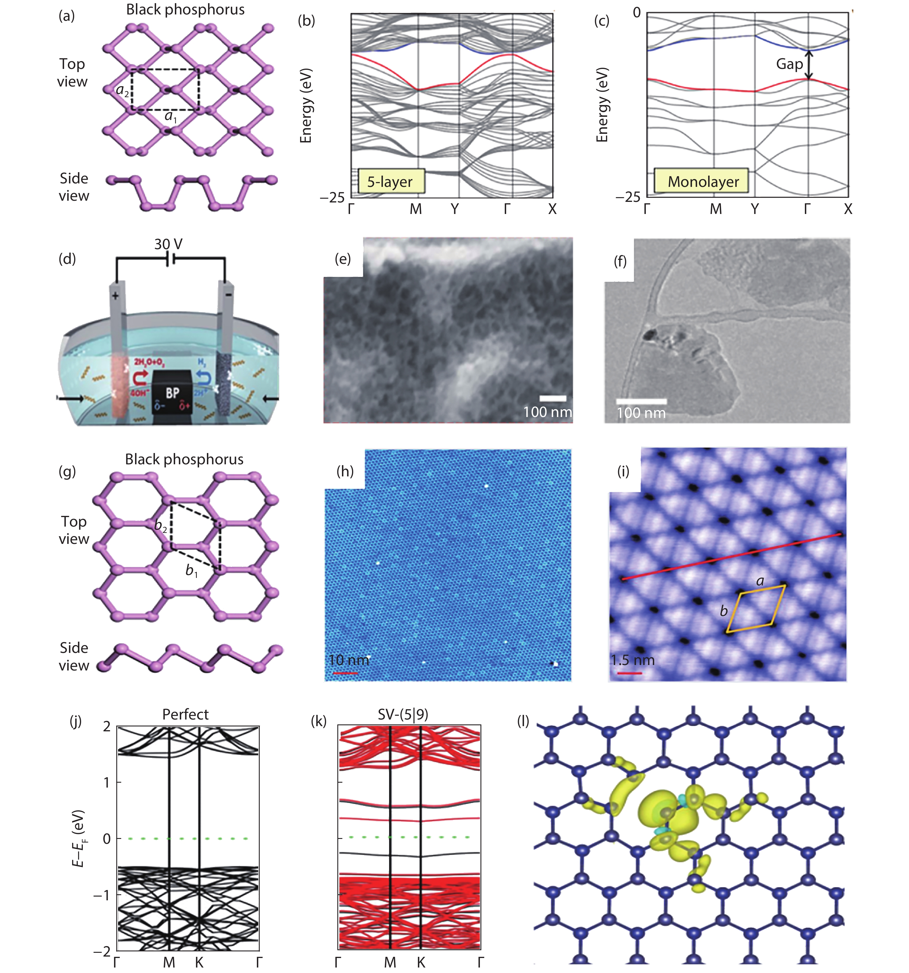
Ma Y Q, Shen C F, Zhang A, et al. Black phosphorus field-effect transistors with work function tunable contacts. ACS Nano, 2017, 11, 7126 doi: 10.1021/acsnano.7b02858 |
| [17] |
Fei R X, Yang L. Strain-engineering the anisotropic electrical conductance of few-layer black phosphorus. Nano Lett, 2014, 14, 2884 doi: 10.1021/nl500935z |
| [18] |
Liu Q, Zhang X W, Abdalla L, et al. Switching a normal insulator into a topological insulator via electric field with application to phosphorene. Nano Lett, 2015, 15, 1222 doi: 10.1021/nl5043769 |
| [19] |
Qiao J S, Kong X H, Hu Z X, et al. High-mobility transport anisotropy and linear dichroism in few-layer black phosphorus. Nat Commun, 2014, 5, 4475 doi: 10.1038/ncomms5475 |
| [20] |
Phuong L T T, Phong T C, Yarmohammadi M. Spin-splitting effects on the interband optical conductivity and activity of phosphorene. Sci Rep, 2020, 10, 9201 doi: 10.1038/s41598-020-65951-9 |
| [21] |
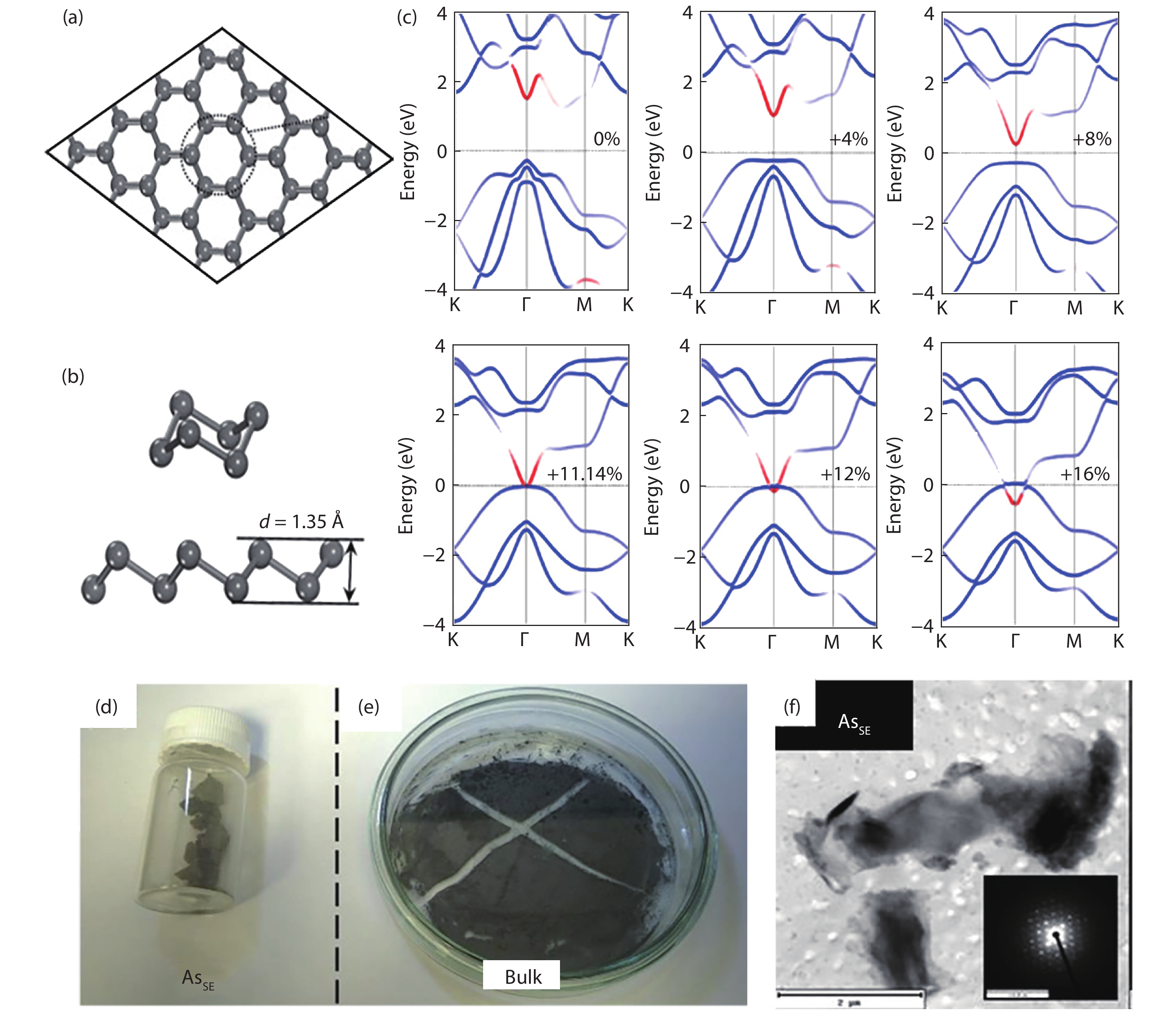
Zhang S L, Yan Z, Li Y F, et al. Atomically thin arsenene and antimonene: Semimetal-semiconductor and indirect-direct band-gap transitions. Angew Chem Int Ed, 2015, 54, 3112 doi: 10.1002/anie.201411246 |
| [22] |
Wada M, Murakami S, Freimuth F, et al. Localized edge states in two-dimensional topological insulators: Ultrathin Bi films. Phys Rev B, 2011, 83, 121310 doi: 10.1103/PhysRevB.83.121310 |
| [23] |
Murakami S. Quantum spin Hall effect and enhanced magnetic response by spin-orbit coupling. Phys Rev Lett, 2006, 97, 236805 doi: 10.1103/PhysRevLett.97.236805 |
| [24] |
Brown A, Rundqvist S. Refinement of the crystal structure of black phosphorus. Acta Crystallogr, 1965, 19, 684 doi: 10.1107/S0365110X65004140 |
| [25] |
Thurn H, Kerbs H. Crystal structure of violet phosphorus. Angew Chem Int Ed, 1966, 5, 1047 doi: 10.1002/anie.196610473 |
| [26] |
Hultgren R, Gingrich N S, Warren B E. The atomic distribution in red and black phosphorus and the crystal structure of black phosphorus. J Chem Phys, 1935, 3, 351 doi: 10.1063/1.1749671 |
| [27] |
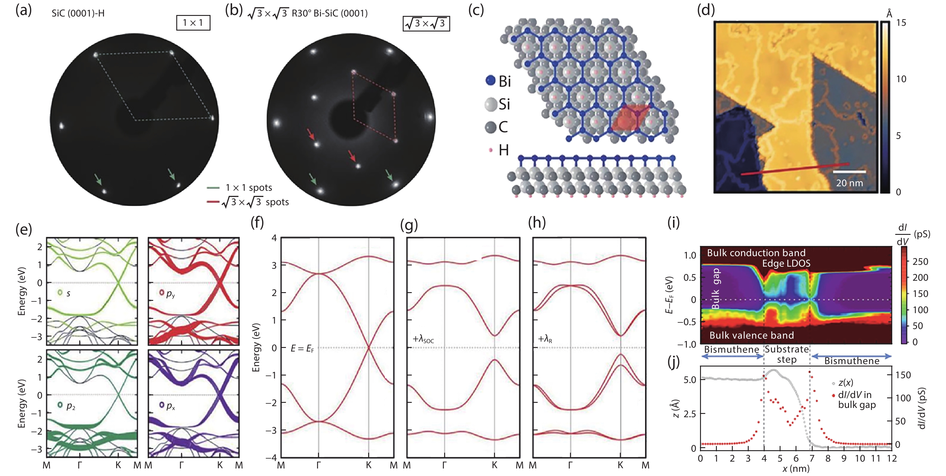
Appalakondaiah S, Vaitheeswaran G, Lebègue S, et al. Effect of van der Waals interactions on the structural and elastic properties of black phosphorus. Phys Rev B, 2012, 86, 035105 doi: 10.1103/PhysRevB.86.035105 |
| [28] |
Fukuoka S, Taen T, Osada T. Electronic structure and the properties of phosphorene and few-layer black phosphorus. J Phys Soc Jpn, 2015, 84, 121004 doi: 10.7566/JPSJ.84.121004 |
| [29] |
Liang L B, Wang J, Lin W Z, et al. Electronic bandgap and edge reconstruction in phosphorene materials. Nano Lett, 2014, 14, 6400 doi: 10.1021/nl502892t |
| [30] |
Kim J S, Jeon P J, Lee J, et al. Dual gate black phosphorus field effect transistors on glass for NOR logic and organic light emitting diode switching. Nano Lett, 2015, 15, 5778 doi: 10.1021/acs.nanolett.5b01746 |
| [31] |
Buscema M, Groenendijk D J, Blanter S I, et al. Fast and broadband photoresponse of few-layer black phosphorus field-effect transistors. Nano Lett, 2014, 14, 3347 doi: 10.1021/nl5008085 |
| [32] |
Li L K, Yu Y J, Ye G J, et al. Black phosphorus field-effect transistors. Nat Nanotechnol, 2014, 9, 372 doi: 10.1038/nnano.2014.35 |
| [33] |
Baboukani A R, Khakpour I, Drozd V, et al. Single-step exfoliation of black phosphorus and deposition of phosphorene via bipolar electrochemistry for capacitive energy storage application. J Mater Chem, 2019, 7, 25548 doi: 10.1039/C9TA09641H |
| [34] |
Liu H, Neal A T, Zhu Z, et al. Phosphorene: an unexplored 2D semiconductor with a high hole mobility. ACS Nano, 2014, 8, 4033 doi: 10.1021/nn501226z |
| [35] |
Xie J, Si M, Yang D, et al. A theoretical study of blue phosphorene nanoribbons based on first-principles calculations. J Appl Phys, 2014, 116, 073704 doi: 10.1063/1.4893589 |
| [36] |
Aierken Y, Cakir D, Sevik C, et al. Thermal properties of black and blue phosphorenes from a first-principles quasiharmonic approach. Phys Rev B, 2015, 92, 081408 doi: 10.1103/PhysRevB.92.081408 |
| [37] |
Ghosh B, Nahas S, Bhowmick S, et al. Electric field induced gap modification in ultrathin blue phosphorus. Phys Rev B, 2015, 91, 115433 doi: 10.1103/PhysRevB.91.115433 |
| [38] |
|
| [39] |
Zhang J L, Zhao S T, Han C, et al. Epitaxial growth of single layer blue phosphorus: A new phase of two-dimensional phosphorus. Nano Lett, 2016, 16, 4903 doi: 10.1021/acs.nanolett.6b01459 |
| [40] |
Wang C, You Y Z, Choi J H. First-principles study of defects in blue phosphorene. Mater Res Express, 2019, 7, 015005 doi: 10.1088/2053-1591/ab59fc |
| [41] |
Wang Y P, Zhang C W, Ji W X, et al. Tunable quantum spin Hall effect via strain in two-dimensional arsenene monolayer. J Phys D, 2016, 49, 055305 doi: 10.1088/0022-3727/49/5/055305 |
| [42] |
Gusmão R, Sofer Z, Bouša D, et al. Innentitelbild: pnictogen (As, Sb, Bi) nanosheets for electrochemical applications are produced by shear exfoliation using kitchen blenders. Angew Chem Int Ed, 2017, 129, 14510 doi: 10.1002/ange.201710278 |
| [43] |
Kamal C, Ezawa M. Arsenene: Two-dimensional buckled and puckered honeycomb arsenic systems. Phys Rev B, 2015, 91, 085423 doi: 10.1103/PhysRevB.91.085423 |
| [44] |
Pizzi G, Gibertini M, Dib E, et al. Performance of arsenene and antimonene double-gate MOSFETs from first principles. Nat Commun, 2016, 7, 12585 doi: 10.1038/ncomms12585 |
| [45] |
Tsai H, Wang S, Hsiao C, et al. Direct synthesis and practical bandgap estimation of multilayer arsenene nanoribbons. Chem Mater, 2016, 28, 425 doi: 10.1021/acs.chemmater.5b04949 |
| [46] |
Ares P, Aguilar-Galindo F, Rodríguez-San-miguel D, et al. Mechanical isolation of highly stable antimonene under ambient conditions. Adv Mater, 2016, 28, 6332 doi: 10.1002/adma.201602128 |
| [47] |
Ji J P, Song X F, Liu J Z, et al. Two-dimensional antimonene single crystals grown by van der Waals epitaxy. Nat Commun, 2016, 7, 13352 doi: 10.1038/ncomms13352 |
| [48] |
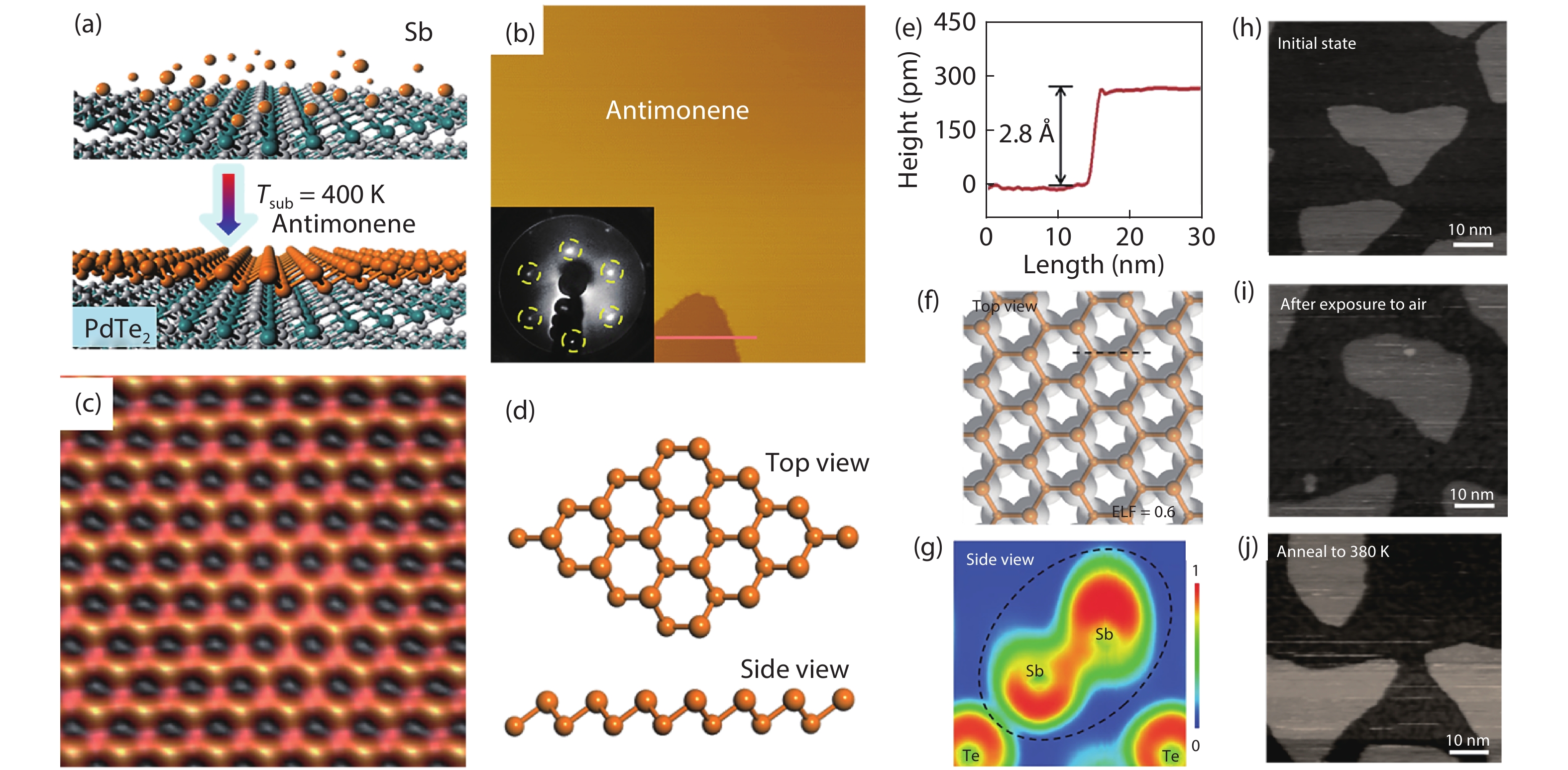
Wu X, Shao Y, Liu H, et al. Epitaxial growth and air-stability of monolayer antimonene on PdTe 2. Adv Mater, 2017, 29, 1605407 doi: 10.1002/adma.201605407 |
| [49] |
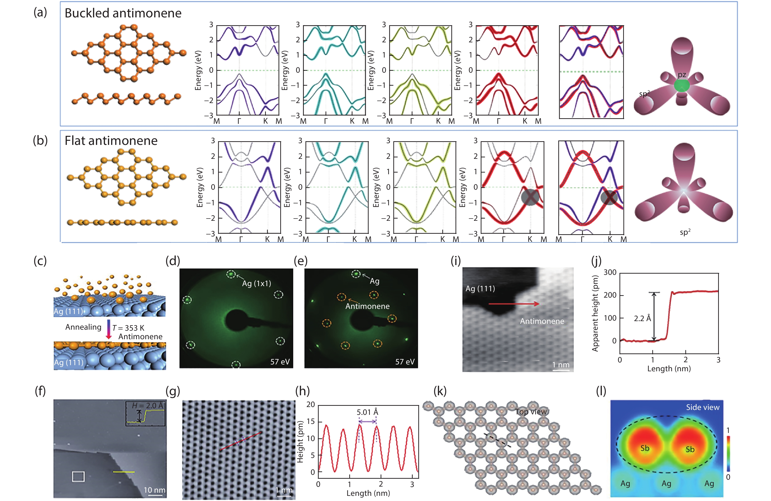
Zhu S, Shao Y, Wang E, et al. Evidence of topological edge states in buckled antimonene monolayers. Nano Lett, 2019, 19, 6323 doi: 10.1021/acs.nanolett.9b02444 |
| [50] |
Shao Y, Liu Z L, Cheng C, et al. Epitaxial growth of flat antimonene monolayer: A new honeycomb analogue of graphene. Nano Lett, 2018, 18, 2133 doi: 10.1021/acs.nanolett.8b00429 |
| [51] |
Zhao A D, Wang B. Two-dimensional graphene-like Xenes as potential topological materials. APL Mater, 2020, 8, 030701 doi: 10.1063/1.5135984 |
| [52] |
Liu Z, Liu C X, Wu Y S, et al. Stable nontrivial Z2 topology in ultrathin Bi (111) films: A first-principles study. Phys Rev Lett, 2011, 107, 136805 doi: 10.1103/PhysRevLett.107.136805 |
| [53] |
Reis F, Li G, Dudy L, et al. Bismuthene on a SiC substrate: A candidate for a high-temperature quantum spin Hall material. Science, 2017, 357, 287 doi: 10.1126/science.aai8142 |
| [54] |
Stühler R, Reis F, Müller T, et al. Tomonaga–Luttinger liquid in the edge channels of a quantum spin Hall insulator. Nat Phys, 2020, 16, 47 doi: 10.1038/s41567-019-0697-z |


 DownLoad: