


 DownLoad:


| Citation: |
Wenzhe Li, Jiandong Fan, Liming Ding. Multidimensional perovskites enhance solar cell performance[J]. Journal of Semiconductors, 2021, 42(2): 020201. doi: 10.1088/1674-4926/42/2/020201
****
W Z Li, J D Fan, L M Ding, Multidimensional perovskites enhance solar cell performance[J]. J. Semicond., 2021, 42(2): 020201. doi: 10.1088/1674-4926/42/2/020201.

|
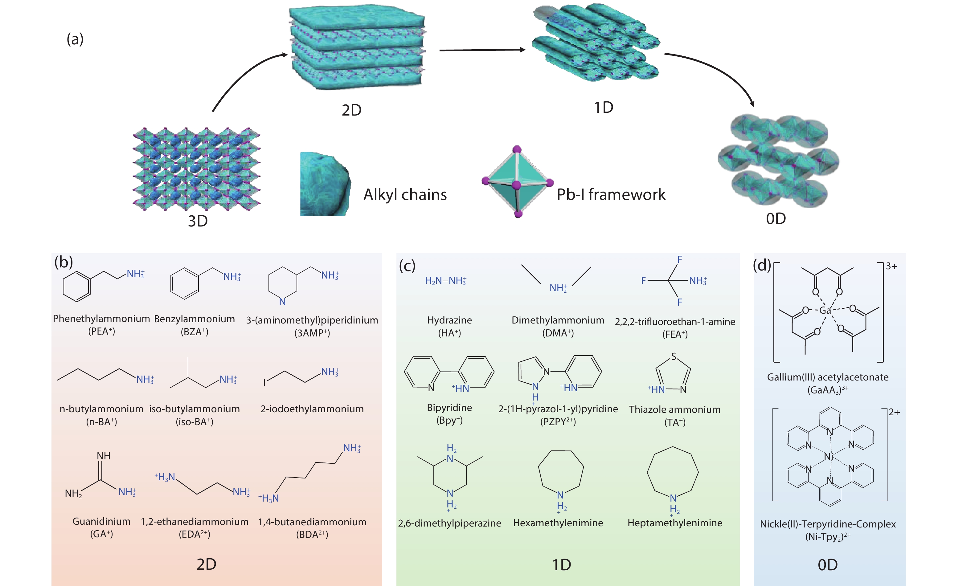
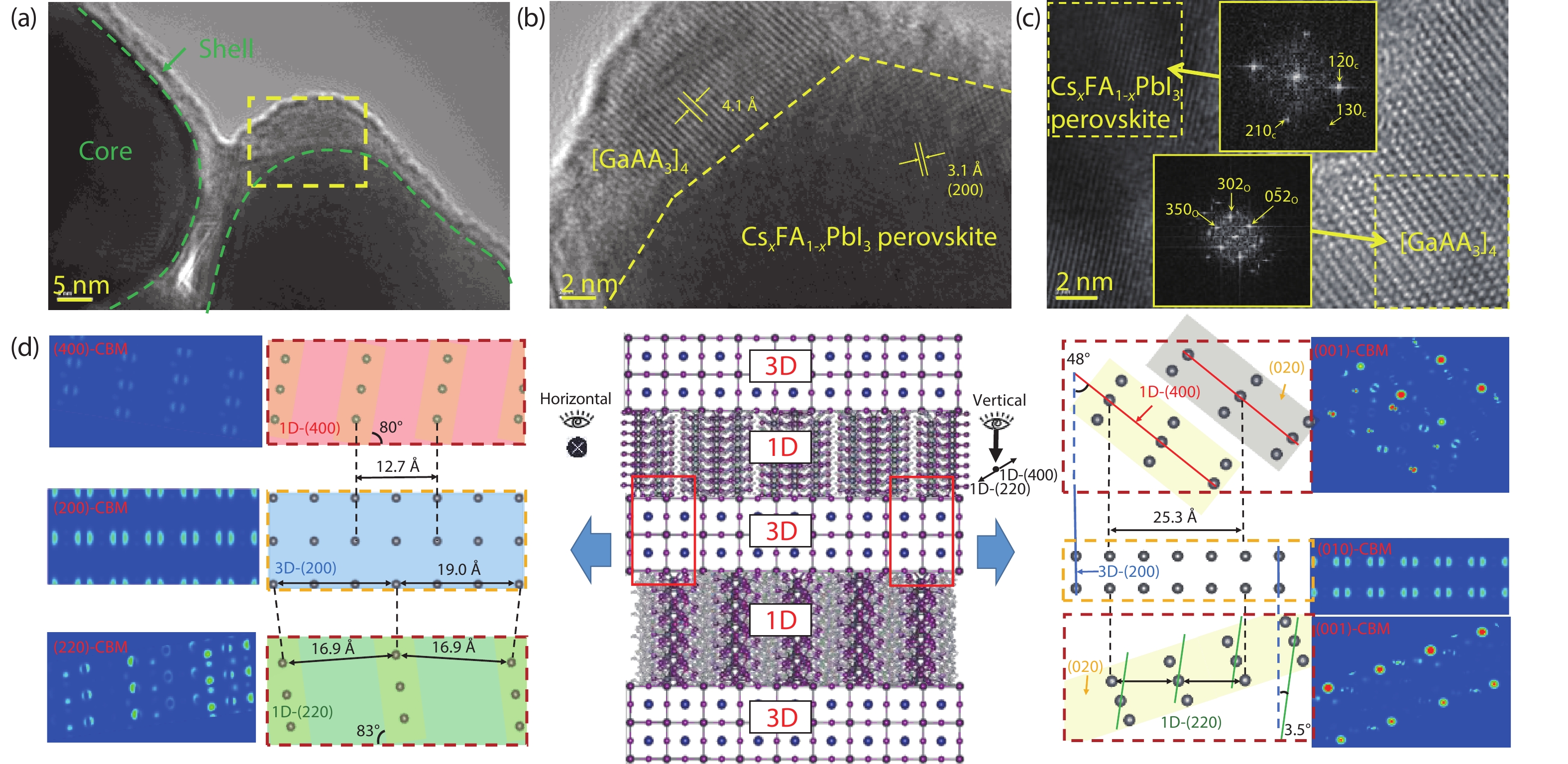
Multidimensional perovskites enhance solar cell performance
DOI: 10.1088/1674-4926/42/2/020201
More Information
-
References
[1] Kojima A, Teshima K, Shirai Y, et al. Organometal halide perovskites as visible-light sensitizers for photovoltaic cells. J Am Chem Soc, 2009, 131, 6050 doi: 10.1021/ja809598r[2] Best research-cell efficiency chart. NREL Photovoltaic Research, 2020[3] Wang R, Mujahid M, Duan Y, et al. A review of perovskites solar cell stability. Adv Funct Mater, 2019, 29, 1808843 doi: 10.1002/adfm.201808843[4] Jeon N J, Noh J H, Yang W S, et al. Compositional engineering of perovskite materials for high-performance solar cells. Nature, 2015, 517, 476 doi: 10.1038/nature14133[5] Fan J, Ma Y, Zhang C, et al. Thermodynamically self-healing 1D–3D hybrid perovskite solar cells. Adv Energy Mater, 2018, 8, 1703421 doi: 10.1002/aenm.201703421[6] Wang S, Chen H, Zhang J, et al. Targeted therapy for interfacial engineering toward stable and efficient perovskite solar cells. Adv Mater, 2019, 31, 1903691 doi: 10.1002/adma.201903691[7] Li W, Zhang W, Van Reenen S, et al. Enhanced UV-light stability of planar heterojunction perovskite solar cells with caesium bromide interface modification. Energy Environ Sci, 2016, 9, 490 doi: 10.1039/C5EE03522H[8] Jeon N J, Noh J H, Kim Y C, et al. Solvent engineering for high-performance inorganic–organic hybrid perovskite solar cells. Nat Mater, 2014, 13, 897 doi: 10.1038/nmat4014[9] Li W, Fan J, Li J, et al. Controllable grain morphology of perovskite absorber film by molecular self-assembly toward efficient solar cell exceeding 17%. J Am Chem Soc, 2015, 137, 10399 doi: 10.1021/jacs.5b06444[10] Qian J, Guo Q, Liu L, et al. A theoretical study of hybrid lead iodide perovskite homologous semiconductors with 0D, 1D, 2D and 3D structures. J Mater Chem A, 2017, 5, 16786 doi: 10.1039/C7TA04008C[11] Zhang X, Wu G, Fu W, et al. Orientation regulation of phenylethylammonium cation based 2D perovskite solar cell with efficiency higher than 11%. Adv Energy Mater, 2018, 8, 1702498 doi: 10.1002/aenm.201702498[12] Spanopoulos I, Hadar I, Ke W, et al. Uniaxial expansion of the 2D Ruddlesden–Popper perovskite family for improved environmental stability. J Am Chem Soc, 2019, 141, 5518 doi: 10.1021/jacs.9b01327[13] Krishna A, Gottis S, Nazeeruddin M K, et al. Mixed dimensional 2D/3D hybrid perovskite absorbers: The future of perovskite solar cells. Adv Funct Mater, 2019, 29, 1806482 doi: 10.1002/adfm.201806482[14] Yu S, Liu H, Wang S, et al. Hydrazinium cation mixed FAPbI3-based perovskite with 1D/3D hybrid dimension structure for efficient and stable solar cells. Chem Eng J, 2021, 403, 125724 doi: 10.1016/j.cej.2020.125724[15] Ke W, Spanopoulos I, Stoumpos C C, et al. Myths and reality of HPbI3 in halide perovskite solar cells. Nat Commun, 2018, 9, 4785 doi: 10.1038/s41467-018-07204-y[16] Gao L, Spanopoulos I, Ke W, et al. Improved environmental stability and solar cell efficiency of (MA, FA)PbI3 perovskite using a wide-band-gap 1D thiazolium lead iodide capping layer strategy. ACS Energy Lett, 2019, 4, 1763 doi: 10.1021/acsenergylett.9b00930[17] Liu P, Xian Y, Yuan W, et al. Lattice-matching structurally-stable 1D@3D perovskites toward highly efficient and stable solar cells. Adv Energy Mater, 2020, 10, 1903654 doi: 10.1002/aenm.201903654[18] Mao L, Guo P, Kepenekian M, et al. Structural diversity in white-light-emitting hybrid lead bromide perovskites. J Am Chem Soc, 2018, 140, 13078 doi: 10.1021/jacs.8b08691[19] Li W, Zhang C, Ma Y, et al. In situ induced core/shell stabilized hybrid perovskites via gallium (iii) acetylacetonate intermediate towards highly efficient and stable solar cells. Energy Environ Sci, 2018, 11, 286 doi: 10.1039/C7EE03113K[20] Zhang Y, Zang M, Yin H, et al. Dimensionally and structurally controllable perovskite single crystals: nickel(ii)–terpyridine complex (Ni–Tpy2)-based perovskites. CrystEngComm, 2020, 22, 1904 doi: 10.1039/C9CE02004G[21] Wang Z, Lin Q, Chmiel F P, et al. Efficient ambient-air-stable solar cells with 2D–3D heterostructured butylammonium-caesium-formamidinium lead halide perovskites. Nat Energy, 2017, 2, 17135 doi: 10.1038/nenergy.2017.135[22] Gangadharan D T, Ma D. Searching for stability at lower dimensions: current trends and future prospects of layered perovskite solar cells. Energy Environ Sci, 2019, 12, 2860 doi: 10.1039/C9EE01591D[23] Grancini G, Nazeeruddin M K. Dimensional tailoring of hybrid perovskites for photovoltaics. Nat Rev Mater, 2019, 4, 4 doi: 10.1038/s41578-018-0065-0 -
Proportional views


