| [1] |
Philipps S. Photovoltaics report. Fraunhofer Institute for Solar Energy Systems, 2019
|
| [2] |
Green M A, Hishikawa Y, Dunlop E D, et al. Solar cell efficiency tables (version 52). Pro Photovolt, 2018, 26(7), 427 doi: 10.1002/pip.3040 |
| [3] |
Alharbi F, Bass J D, Salhi A, et al. Abundant non-toxic materials for thin film solar cells: Alternative to conventional materials. Renew Energ, 2011, 36(10), 2753 doi: 10.1016/j.renene.2011.03.010 |
| [4] |
Jean J, Brown P R, Jaffe R L, et al. Pathways for solar photovoltaics. Energy Environ Sci, 2015, 8(4), 1200 doi: 10.1039/C4EE04073B |
| [5] |
Lei H, Chen J, Tan Z, et al. Review of recent progress in antimony chalcogenide-based solar cells: Materials and devices. Solar RRL, 2019, 3(6), 1900026 doi: 10.1002/solr.201900026 |
| [6] |
Mavlonov A, Razykov T, Raziq F, et al. A review of Sb 2Se 3 photovoltaic absorber materials and thin-film solar cells. Sol Energy, 2020, 201, 227 doi: 10.1016/j.solener.2020.03.009 |
| [7] |
Wong L H, Zakutayev A, Major J D, et al. Emerging inorganic solar cell efficiency tables (Version 1). J Phys: Energy, 2019, 1(3), 032001 doi: 10.1088/2515-7655/ab2338 |
| [8] |
Yu L, Kokenyesi R S, Keszler D A, et al. Inverse design of high absorption thin-film photovoltaic materials. Adv Energy Mater, 2013, 3(1), 43 doi: 10.1002/aenm.201200538 |
| [9] |
Phillips L J, Savory C N, Hutter O S, et al. Current enhancement via a TiO 2 window layer for CSS Sb 2Se 3 solar cells: Performance limits and high VOC. IEEE J Photovolt, 2019, 9(2), 544 doi: 10.1109/JPHOTOV.2018.2885836 |
| [10] |
Li Z, Liang X, Li G, et al. 9.2%-efficient core-shell structured antimony selenide nanorod array solar cells. Nat Commun, 2019, 10(1), 125 doi: 10.1038/s41467-018-07903-6 |
| [11] |
Liu C, Wang L, Tang Y, et al. Vertical single or few-layer MoS 2 nanosheets rooting into TiO 2 nanofibers for highly efficient photocatalytic hydrogen evolution. Appl Catal B, 2015, 164, 1 doi: 10.1016/j.apcatb.2014.08.046 |
| [12] |
Chuang H J, Chamlagain B, Koehler M, et al. Low-resistance 2D/2D ohmic contacts: A universal approach to high-performance WSe 2, MoS 2, and MoSe 2 transistors. Nano Lett, 2016, 16(3), 1896 doi: 10.1021/acs.nanolett.5b05066 |
| [13] |
Zhao M, Su J, Zhao Y, et al. Sodium-mediated epitaxial growth of 2D ultrathin Sb 2Se 3 flakes for broadband photodetection. Adv Funct Mater, 2020, 30(13), 1909849 doi: 10.1002/adfm.201909849 |
| [14] |
Chen Z G, Shi X, Zhao L D, et al. High-performance SnSe thermoelectric materials: Progress and future challenge. Prog Mater Sci, 2018, 97, 283 doi: 10.1016/j.pmatsci.2018.04.005 |
| [15] |
Wu T, Zhang H. Piezoelectricity in two-dimensional materials. Angew Chem Int Ed, 2015, 54(15), 4432 doi: 10.1002/anie.201411335 |
| [16] |
Niu S, Joe G, Zhao H, et al. Giant optical anisotropy in a quasi-one-dimensional crystal. Nat Photonics, 2018, 12(7), 392 doi: 10.1038/s41566-018-0189-1 |
| [17] |
Tian H, Tice J, Fei R, et al. Low-symmetry two-dimensional materials for electronic and photonic applications. Nano Today, 2016, 11(6), 763 doi: 10.1016/j.nantod.2016.10.003 |
| [18] |
Donnay J D H, Harker D. A new law of crystal morphology extending the law of Bravais. Am Mineral, 1937, 22(5), 446
|
| [19] |
Brandt R E, Poindexter J R, Gorai P, et al. Searching for “defect-tolerant” photovoltaic materials: Combined theoretical and experimental screening. Chem Mater, 2017, 29(11), 4667 doi: 10.1021/acs.chemmater.6b05496 |
| [20] |
Othonos A. Probing ultrafast carrier and phonon dynamics in semiconductors. J App Phys, 1998, 83(4), 1789 doi: 10.1063/1.367411 |
| [21] |
Hutter E M, Gélvez-Rueda M C, Osherov A, et al. Direct–indirect character of the bandgap in methylammonium lead iodide perovskite. Nat Mater, 2016, 16, 115 doi: 10.1038/nmat4765 |
| [22] |
Saliba M, Correa-Baena J P, Wolff C M, et al. How to make over 20% efficient perovskite solar cells in regular (n–i–p) and inverted (p–i–n) architectures. Chem Mater, 2018, 30(13), 4193 doi: 10.1021/acs.chemmater.8b00136 |
| [23] |
Walsh A, Zunger A. Instilling defect tolerance in new compounds. Nat Mater, 2017, 16, 964 doi: 10.1038/nmat4973 |
| [24] |
Vidal J, Lany S, d’Avezac M, et al. Band-structure, optical properties, and defect physics of the photovoltaic semiconductor SnS. Appl Phys Lett, 2012, 100(3), 032104 doi: 10.1063/1.3675880 |
| [25] |
Huang Y, Wang C, Chen X, et al. First-principles study on intrinsic defects of SnSe. RSC Advances, 2017, 7(44), 27612 doi: 10.1039/C7RA03367B |
| [26] |
Han D, Du M H, Dai C M, et al. Influence of defects and dopants on the photovoltaic performance of Bi 2S 3: first-principles insights. J Mater Chem A, 2017, 5(13), 6200 doi: 10.1039/C6TA10377D |
| [27] |
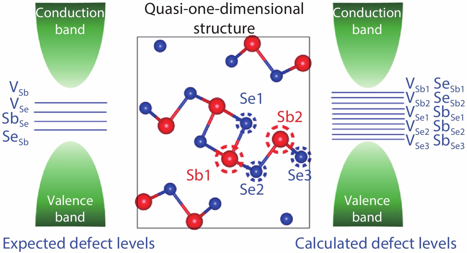
Huang M, Xu P, Han D, et al. Complicated and unconventional defect properties of the quasi-one-dimensional photovoltaic semiconductor Sb 2Se 3. ACS Appl Mater Inter, 2019, 11(17), 15564 doi: 10.1021/acsami.9b01220 |
| [28] |
Qiao J, Kong X, Hu Z X, et al. High-mobility transport anisotropy and linear dichroism in few-layer black phosphorus. Nat Commun, 2014, 5(1), 4475 doi: 10.1038/ncomms5475 |
| [29] |
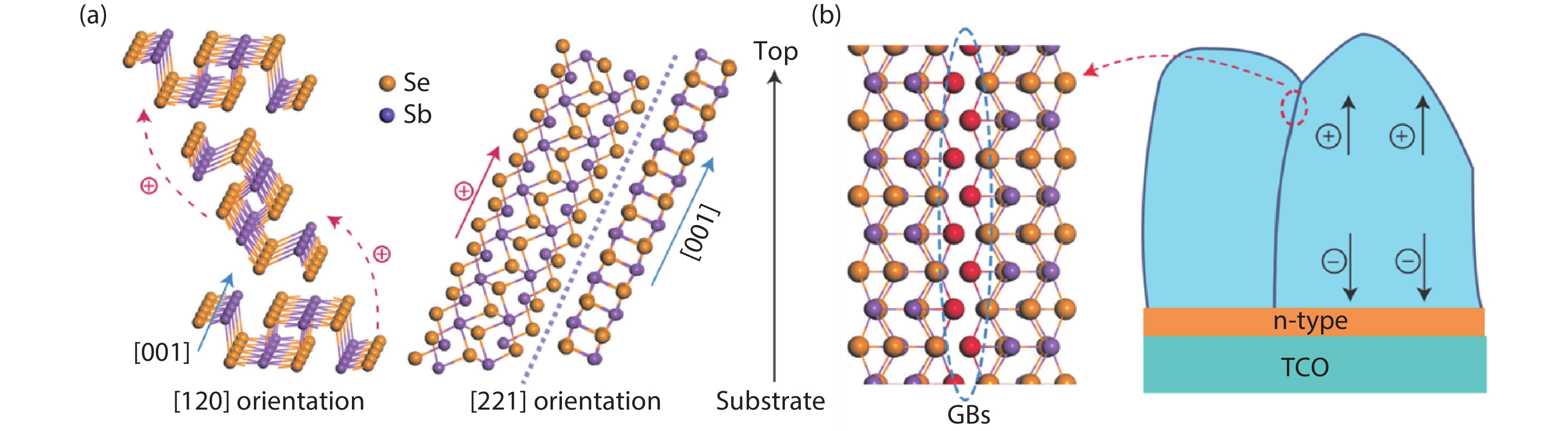
Zhou Y, Wang L, Chen S, et al. Thin-film Sb 2Se 3 photovoltaics with oriented one-dimensional ribbons and benign grain boundaries. Nat Photonics, 2015, 9(6), 409 doi: 10.1038/nphoton.2015.78 |
| [30] |
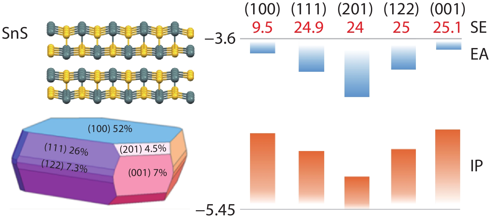
Novoselov K S, Mishchenko A, Carvalho A, et al. 2D materials and van der Waals heterostructures. Science, 2016, 353(6298), aac9439 doi: 10.1126/science.aac9439 |
| [31] |
Welch A W, Baranowski L L, Zawadzki P, et al. Accelerated development of CuSbS 2 thin film photovoltaic device prototypes. Pro Photovoltaics, 2016, 24(7), 929 doi: 10.1002/pip.2735 |
| [32] |
Kirchartz T, Rau U. What makes a good solar cell. Adv Energy Mater, 2018, 8(28), 1703385 doi: 10.1002/aenm.201703385 |
| [33] |
Gilbert L R, Van Pelt B, Wood C. The thermal activation energy of crystalline Sb 2Se 3. J Phys Chem Solids, 1974, 35(12), 1629 doi: 10.1016/S0022-3697(74)80175-7 |
| [34] |
Chen Y, Sun Y, Peng J, et al. Tailoring organic cation of 2D air-Stable organometal halide perovskites for highly efficient planar solar cells. Adv Energy Mater, 2017, 7(18), 1700162 doi: 10.1002/aenm.201700162 |
| [35] |
Tsai H, Nie W, Blancon J C, et al. High-efficiency two-dimensional Ruddlesden–Popper perovskite solar cells. Nature, 2016, 536, 312 doi: 10.1038/nature18306 |
| [36] |
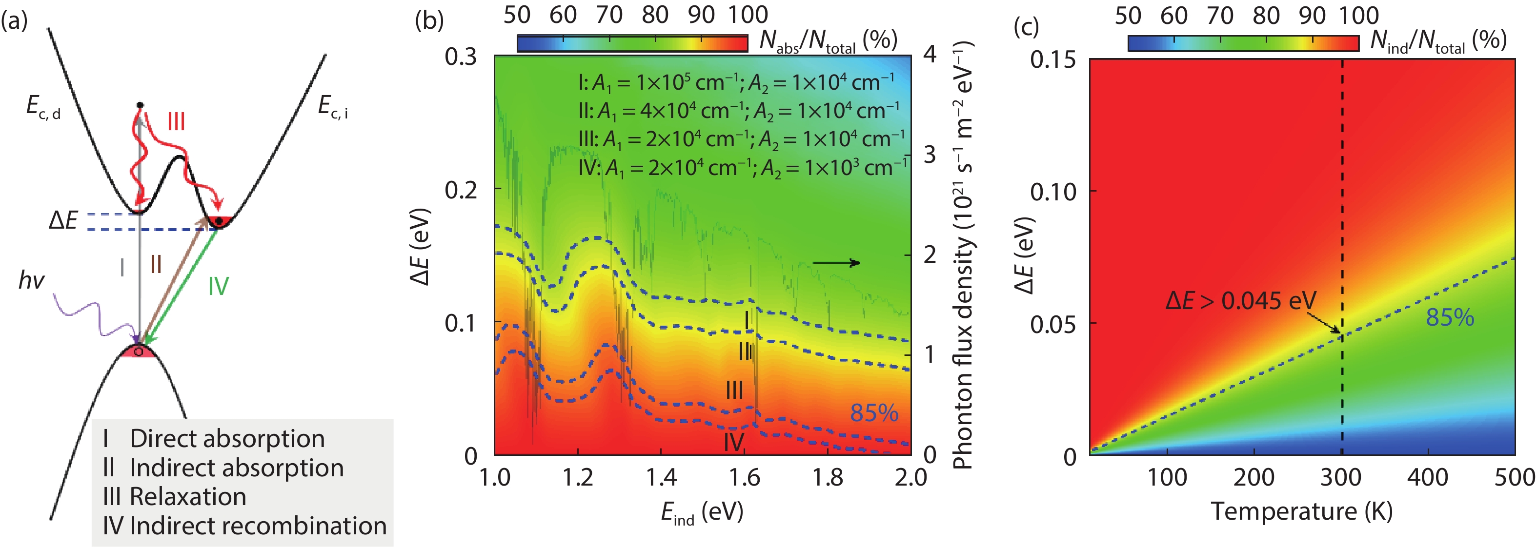
Nassary M M. Temperature dependence of the electrical conductivity, Hall effect and thermoelectric power of SnS single crystals. J Alloy Compd, 2005, 398(1), 21 doi: 10.1016/j.jallcom.2005.02.025 |
| [37] |
Sinsermsuksakul P, Sun L, Lee S W, et al. Overcoming efficiency limitations of SnS-based solar cells. Adv Energy Mater, 2014, 4(15), 1400496 doi: 10.1002/aenm.201400496 |
| [38] |
Zhao L D, Tan G, Hao S, et al. Ultrahigh power factor and thermoelectric performance in hole-doped single-crystal SnSe. Science, 2016, 351(6269), 141 doi: 10.1126/science.aad3749 |
| [39] |
Welch A W, Baranowski L L, Peng H, et al. Trade-offs in thin film solar cells with layered chalcostibitephotovoltaic absorbers. Adv Energy Mater, 2017, 7(11), 1601935 doi: 10.1002/aenm.201601935 |
| [40] |
Ramasamy K, Sims H, Butler W H, et al. Mono-, few-, and multiple layers of copper antimony sulfide (CuSbS 2): A ternary layered sulfide. J Am Chem Soc, 2014, 136(4), 1587 doi: 10.1021/ja411748g |
| [41] |
Banu S, Ahn S J, Ahn S K, et al. Fabrication and characterization of cost-efficient CuSbS 2 thin film solar cells using hybrid inks. Sol Energ Mat Sol C, 2016, 151, 14 doi: 10.1016/j.solmat.2016.02.013 |
| [42] |
Kautek W. Electronic mobility anisotropy of layered semiconductors: transversal photoconductivity measurements at n-MoSe 2. J Phys C, 1982, 15(16), L519 doi: 10.1088/0022-3719/15/16/002 |
| [43] |
Chen Z, Liu H, Chen X, et al. Wafer-size and single-crystal MoSe 2 atomically thin films grown on GaN substrate for light emission and harvesting. ACS Appl Mater Inter, 2016, 8(31), 20267 doi: 10.1021/acsami.6b04768 |
| [44] |
Evans B, Young P. Optical absorption and dispersion in molybdenum disulphide. Proc R Soc London Ser A, 1965, 284(1398), 402 doi: 10.1098/rspa.1965.0071 |
| [45] |
Wi S, Kim H, Chen M, et al. Enhancement of photovoltaic response in multilayer MoS 2 induced by plasma doping. ACS Nano, 2014, 8(5), 5270 doi: 10.1021/nn5013429 |
| [46] |
Kyriakos D S, Anagnostopoulos A N. Electrical conductivity of layered GeSe related to extended faults. J App Phys, 1985, 58(10), 3917 doi: 10.1063/1.335613 |
| [47] |
Xue D J, Liu S C, Dai C M, et al. GeSe thin-film solar cells fabricated by self-regulated rapid thermal sublimation. J Am Chem Soc, 2017, 139(2), 958 doi: 10.1021/jacs.6b11705 |
| [48] |
Chakraborty B R, Ray B, Bhattacharya R, et al. Magnetic and electric properties of antimony selenide (Sb 2Se 3) crystals. J Phys Chem Solids, 1980, 41(8), 913 doi: 10.1016/0022-3697(80)90037-2 |
| [49] |
Roy B, Chakraborty B R, Bhattacharya R, et al. Electrical and magnetic properties of antimony sulphide (Sb 2S 3) crystals and the mechanism of carrier transport in it. Solid State Commun, 1978, 25(11), 937 doi: 10.1016/0038-1098(78)90306-X |
| [50] |
Choi Y C, Lee D U, Noh J H, et al. Highly improved Sb 2S 3 sensitized-inorganic–organic heterojunction solar cells and quantification of traps by deep-level transient spectroscopy. Adv Function Mater, 2014, 24(23), 3587 doi: 10.1002/adfm.201304238 |
| [51] |
Wang X, Tang R, Jiang C, et al. Manipulating the electrical properties of Sb 2(S,Se) 3 film for high-efficiency solar cell. Adv Energy Mater, 2020, 10, 2002341 doi: 10.1002/aenm.202002341 |
| [52] |
Cantarero A, Martinez-Pastor J, Segura A, et al. Transport properties of bismuth sulfide single crystals. Phys Rev B, 1987, 35(18), 9586 doi: 10.1103/PhysRevB.35.9586 |
| [53] |
Song H, Zhan X, Li D, et al. Rapid thermal evaporation of Bi 2S 3 layer for thin film photovoltaics. Sol Energ Mat Sol C, 2016, 146, 1 doi: 10.1016/j.solmat.2015.11.019 |
| [54] |
Yoshida M, Yamanaka K, Hamakawa Y. Semiconducting and dielectric properties of c-axia oriented SbSI thin film. Jpn J Appl Phys, 1973, 12(11), 1699 doi: 10.1143/JJAP.12.1699 |
| [55] |
Nie R, Yun H S, Paik M J, et al. Efficient solar cells based on light-harvesting antimony sulfoiodide. Adv Energy Mater, 2018, 8(7), 1701901 doi: 10.1002/aenm.201701901 |
| [56] |
Hoye R L Z, Lee L C, Kurchin R C, et al. Strongly enhanced photovoltaic performance and defect physics of air-stable bismuth oxyiodide (BiOI). Adv Mater, 2017, 29(36), 1702176 doi: 10.1002/adma.201702176 |
| [57] |
Todorov T K, Singh S, Bishop D M, et al. Ultrathin high band gap solar cells with improved efficiencies from the world's oldest photovoltaic material. Nat Commun, 2017, 8(1), 682 doi: 10.1038/s41467-017-00582-9 |
| [58] |
Koma A. New epitaxial growth method for modulated structures using van der Waals interactions. Surf Sci, 1992, 267(1), 29 doi: 10.1016/0039-6028(92)91081-L |
| [59] |
Yang B, Wang C, Yuan Z, et al. Hydrazine solution processed CuSbSe 2: Temperature dependent phase and crystal orientation evolution. Sol Energ Mat Sol C, 2017, 168, 112 doi: 10.1016/j.solmat.2017.04.030 |
| [60] |
Jaccodine R. Surface energy of germanium and silicon. J Electrochem Soc, 1963, 110(6), 524 doi: 10.1149/1.2425806 |
| [61] |
Stevanović V, Hartman K, Jaramillo R, et al. Variations of ionization potential and electron affinity as a function of surface orientation: The case of orthorhombic SnS. Appl Phys Lett, 2014, 104(21), 211603 doi: 10.1063/1.4879558 |
| [62] |
Venables J A,Spiller G D T. Surface mobilities on solid materials. Boston, MA: Springer, 1983
|
| [63] |
Rincón M E, Sánchez M, George P J, et al. Comparison of the properties of bismuth sulfide thin films prepared by thermal evaporation and chemical bath deposition. J Solid State Chem, 1998, 136(2), 167 doi: 10.1006/jssc.1997.7670 |
| [64] |
Razykov T M, Shukurov A X, Atabayev O K, et al. Growth and characterization of Sb 2Se 3 thin films for solar cells. Sol Energy, 2018, 173, 225 doi: 10.1016/j.solener.2018.07.082 |
| [65] |
Mayon Y S, White T P, Wang R, et al. Evaporated and solution deposited planar Sb 2S 3 solar cells: A comparison and its significance. Phys Status Solid A, 2016, 213(1), 108 doi: 10.1002/pssa.201532438 |
| [66] |
Nwofe P A, Reddy K T R, Sreedevi G, et al. Single phase, large grain, p-conductivity-type SnS layers produced using the thermal evaporation method. Energy Procedia, 2012, 15, 354 doi: 10.1016/j.egypro.2012.02.043 |
| [67] |
Zhang M, Lv L, Wei Z, et al. Thermal evaporation growth of topological insulator Bi 2Se 3 thin films. Mater Lett, 2014, 123, 87 doi: 10.1016/j.matlet.2014.02.108 |
| [68] |
Solayappan N, Raina K K, Pandey R K, et al. Role of antimony sulfide buffer layers in the growth of ferroelectric antimony sulfo-iodide thin films. J Mater Res, 1997, 12(3), 825 doi: 10.1557/JMR.1997.0120 |
| [69] |
Varghese J, O’Regan C, Deepak N, et al. Surface roughness assisted growth of vertically oriented ferroelectric SbSI nanorods. Chem Mater, 2012, 24(16), 3279 doi: 10.1021/cm301928w |
| [70] |
Kondrotas R, Zhang J, Wang C, et al. Growth mechanism of Sb 2Se 3 thin films for photovoltaic application by vapor transport deposition. Sol Energ Mat Sol C, 2019, 199, 16 doi: 10.1016/j.solmat.2019.04.024 |
| [71] |
Mavlonov A, Shukurov A, Raziq F, et al. Structural and morphological properties of PLD Sb 2Se 3 thin films for use in solar cells. Sol Energy, 2020, 208, 451 doi: 10.1016/j.solener.2020.08.004 |
| [72] |
Lim D, Suh H, Suryawanshi M, et al. Kinetically controlled growth of phase-pure SnS absorbers for thin film solar cells: Achieving efficiency near 3% with long-term stability using an SnS/CdS heterojunction. Adv Energy Mater, 2018, 8(10), 1702605 doi: 10.1002/aenm.201702605 |
| [73] |
Chen C, Tang J. Open-crcuit voltage loss of antimony chalcogenide solar cells: status, origin, and possible solutions. ACS Energy Lett, 2020, 5(7), 2294 doi: 10.1021/acsenergylett.0c00940 |
| [74] |
Liang G X, Luo Y D, Chen S, et al. Sputtered and selenized Sb 2Se 3 thin-film solar cells with open-circuit voltage exceeding 500 mV. Nano Energy, 2020, 73, 104806 doi: 10.1016/j.nanoen.2020.104806 |
| [75] |
Hobson T D C, Phillips L J, Hutter O S, et al. Isotype heterojunction solar cells using n-type Sb 2Se 3 thin films. Chem Mater, 2020, 32(6), 2621 doi: 10.1021/acs.chemmater.0c00223 |


 DownLoad: